Note: Descriptions are shown in the official language in which they were submitted.
- 2175035
-WO 95112157 PCTIUS94112378
-1-
SWITCHMODE AC POWER CONTR LLER
This invention relates to AC power controllers, and
more particularly concerns such controllers for varying the
alternating electromotive force ("voltage") output applied to
a load while maintaining the sinusoidal A.C. wave-farm of the
output voltage. The invention finds its primary application
in the control of the intensity of a lamp in light dimming
applications.
BACRGROOND OF THE INVEIZTIOIJ
The light dimming function has been implemented in
a variety of ways. Several of these implementations of dimming
techniques provide a variable sinusoidal output voltage. The
advantage of providing a variable sinusoidal output voltage is
a lower noise level during operation, and this applies to both
electrical and mechanical noise. The electrical noise in this
sense refers mainly to signals back-propagated into the AC
power supply that distort its almost pure sinusoidal wave-form.
One power control method that preserves the
sinusoidal wave-form is to provide a high power variable
resistor to control the current through a lamp and hence the
intensity of the lamp. This method can be used in both direct
current and alternating current electric networks. The
resistor, however, dissipates large amounts of power as heat,
resulting in a low overall efficiency.
Another method uses a manual or motor driven variable
voltage transformer to deliver a controllable voltage to a
lamp. Although the efficiency of this method is relatively
high, the size, weight and cost of the equipment makes this
method quite unsuitable for light dimming applications,
especially when more than one variable voltage transformer has
to be synchronized for parallel control of a number of lamps.
Further, the cost of the motor controlling circuitry and the
overall slow response when fast changing lamp intensity is
required constitute additional disadvantages. The variable
voltage transformer, like any other mechanical device, is
W0 95/12157 PCTlUS94112378
217~(~3
-z-
subject to mechanical wear. An additional cost is incurred for
an external fuse or circuit breaker to protect the internal
winding from self destruction during an output overload or
short-circuit. ,
A still further example of a method for controlling
the intensity of a lamp is a multiple tap transformer. This
has been used to provide output voltages in a number of
increments equal to the number of taps. This method is similar
to the variable voltage transformer method described above, and
suffers from the same limitations.
In still another method, variations of the generic
D class amplifier electronic power circuit has been used to
synthesize a variable output sinusoidal voltage. U.S. Patent
No. 5,018,058 issued to Ionescu et al, describes a dual
conversion high frequency switching AC controller. After the
first conversion, two 60 Hz modulated unipolar variable voltage
sources provide the voltages required by the output stage,
designed along the class D amplifier guidelines. It is
provided, however, that both unipolar voltage sources used by
the output stage are not DC, but rather two half cycle
waveforms, of a higher magnitude than the input voltage.
Although this method could in principle be used for a light
dimmer, it represents expensive overkill. Its accurate
reconstruction of an ideal sinusoidal output waveform virtually
independent of the input -voltage waveform will impose a
relative high manufacturing cost for light dimming
applications, where an ideal sinusoidal output waveform is not
necessary.
Aside from these sine wave maintaining systems, a
relatively newer class of light dimmers uses triacs or silicon
controlled rectifiers (SCRs) operating under what is
generically called "variable phase angle. modulation". In these
methods, the triac is turned on at different phases of each
half cycle of the sinusoidal wave form. This results in a
large current surge through the lamp each time the turn-on
event occurs. Since the internal resistance of the lamp varies
2175035
WO 95!12157 PCTIUS94/12375
-3-
with the temperature of the lamp or with the light intensity
there is an increase in the magnitude of the turn-on current
surge due to the fact that at each turn-on point of the triac,
the filament is colder than after a number on milliseconds (or
fractions of seconds for some higher power lamps) of continuous
operation. This high turn-on surge current causes major
mechanical and electric noise injected back into the electric
network. This is a serious problem at the high current levels
that would be present in a lighting system for a theater or an
outdoor lighting situation such as at a ball park.
Due to the sharp electromagnetic field variations
caused by triacs or SCR's and sharp thermal expansion of the
filament at the turn-on point, mechanical noise is generated
by the filament. This produces a train of 12o Hz (100 Hz for
50 Hz electric systems) vibrations. The intensity of such
vibrations varies with the type and power level of the lamp and
with the turn-on moment during each half cycle. Thus these
triac systems implemented in large power consuming lighting
situations result in annoying acoustic noise and severely
detrimental electrical noise feedback into the power supply
lines.
As a result these systems have had to go to the
expense of providing equipment to attempt to reduce or
eliminate both types of noise. For example, a large output
inductor has been connected in series with the lamp to limit
the di/dt factor by distributing the surge current at the turn-
on point over a period of time of several hundreds
microseconds. There is a limit to the period of time over
which the surge may be smoothed without sacrificing the overall
dimmer efficiency. A typical value is that the time period
cannot exceed a one millisecond and this value is inversely
. proportional to the lamp power level. A higher power lamp will
require a longer period of time for distributing the turn-on
surge current than a low power lamp. The long time period
associated with a system tuned for high power lamps will still
cause significant amounts of mechanical and electrical noise,
215035
WO 95/12157 PCTIUS94I12378
-4-
specially when a lower power lamp is used.
U.S. Patent No. 4,633,161 issued to Callahan et al,
describes an inductorless phase control dimmer. This patent
is directed to the elimination of the filter inductor from the
output stage of the dimmer. A pair of MOSFETS is slowly turned
on resulting in a low di/dt factor and practically very little
mechanical and electric noise. The major disadvantage of this
invention is the large amount of power dissipation while both
MOSFETS operate in linear mode during their turn on process.
The Rds on of the MOSFETS increases -with the temperature,
further increasing the amount of dissipated power. A large
heat sink is needed to properly dissipate the resulting heat.
In the case of an output overload or short circuit, the absence
of an inductor will cause a sharp output current increase,
which may reach fatal levels before the internal current
limiting system can react and turn off the MOSFETS.
BRIEF DESCRIPTION OF THE INVENTION
The present invention provides a solid state, high
frequency AC switch-mode power controller which avoids the
difficulties and disadvantages of prior AC power controllers
employed in light dimming applications. Its output waveform
is identical, within a reasonable margin of error, with the
waveform of the input AC line voltage. The invention comprises
an RFI filter interface to the input AC line, which limits the
magnitude of switching transients injected back into the AC
line.
WO 95112157 ~ ~ ~ 5 0 3 5 PCT~S94/12378
-5-
BRIEF DESCRIPTION OF THE DRANINGS
Fig. 1 is a basic simplified block diagram of this
invention.
Fig. 2 is a block diagram of a preferred embodiment.
Fig. -3 shows a variety of signals, describing the
switchmode operation of the preferred embodiment.
Fig. 4 describes the operation of the output overload
and short-circuit protection block and the temporary current
limiting process.
Fig. 5 shows a possible circuit configuration of the
AC solid state switch and synchro-flywheel used in the
preferred embodiment.
Fig. 6 shows another possible circuit configuration
of the AC solid state switch.
Fig. 7 shows two possible locations of the current
sensor, either as used in the preferred embodiment, or as a low
value current sense resistor.
D1;TATLED DESCRTPTION OF A PREFERRED ENBODT~um
A preferred embodiment of the system of the present
invention will now be described with reference to the figures.
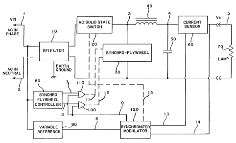
Fig. 1 depicts a basic simplified block diagram of
the invention showing its principal elements. An AC solid
state switch 20 supplies the load current, with its on/off
ratio (duty cycle) set according to the desired output voltage
on line 5 and load current requirements. The invention also
comprises an output filtering and wave-form re-shaping stage,
comprising of an inductor ~Q and a filter capacitor ~0.
The invention further comprises a synchro-flywheel
3~ that allows the discharge of the energy stored in the output
inductor. The synchro-flywheel system is reversed biased
during the time the AC solid state switch 20 is on and direct
biased when the AC solid state switch is off. The inductor _40
discharge current travels through a lamp 60, the synchro
flywheel ~Q andthe inductor 20. During the inductor discharge
portion of the cycle, the output voltage maintains the same
wo ssnzis~ rcTms9anzs~s
217x035
-6-
polarity as the output voltage encountered during the time the
AC solid-state switch 20was on, increasing the overall system
efficiency and reducing the output voltage ripple. Thus it may
be seen that the purpose of the synchro-flywheel is to .
discharge the inductor gQ during the time off cycle of the
switch 2~1. As shown in Fig. S, the synchro-flywheel comprises
two common source MOSFETS. Depending upon the polarity of the
AC signal a conductive path is established either through the
upper diode and lower MOSFET or vice versa.
An output current sensing device ~0 turns off and
resets the AC solid state switch 20 for a limited period of
time, providing a temporary output current on line 5_ capable
of accommodating lamps with large thermal lags. The current
is shut off after the limited period of time has expired, to
prevent overloading or short-circuiting.
The more detailed depiction of a preferred embodiment -
is shown in Fig. 2, which has corresponding elements similarly
numbered. The description of a preferred embodiment will
therefore be carried out with reference to Fig. 2.
Fig. 2 is a functional system block diagram,
comprising eleven functional blocks. More particularly, the
system comprises an AC power controller having an RFI filter
~0 that reduces the magnitude of high frequency switching
electric noise and transients injected by the system back into
the AC line. A variable reference receives the AC current from
the AC line ~ and controls its amplitude on line 6_, from zero
to a maximum value, corresponding to a zero to 100% output
intensity of the lamp 70. - The variable reference can be a
simple potentiometer, a DC gain controlled operational
amplifier or an "n" bit digitally gain-controlled operational
amplifier. The number of bits must be selected to allow the
desired light control increment.
The synchronized modulator ~ compares the variable
reference signal on line ø and the output voltage signal or
feedback signal on line,~g, operating in a manner synchronized
by the polarity of the AC line voltage and designed for proper
2175035
W O 95!12157 PCT/U594/12378
operation in all quadrants. If both reference 6 and output
voltage signal 3,g are positive, both signals are compared by
the synchronized modulator X20 with regard to their
instantaneous values. As shown in Fig. 3, the duration of the
control signal pulses on line ,~,~, as depicted in the left
section of the graph, is increased if the output (feedback)
voltage signal ~ is lower than the reference signal f, or
decreased, as depicted in the right section of the graph, if
the output voltage signal 14 is higher than the reference
signal . In this case, the resulting internal signal on line
controlling the duration of AC solid state switch _20 is a
series of control pulses whose width is proportional to the
difference between the reference signal ~ and output voltage
signal ~4. The signals from the synchronized modulator 3,20
along line 15 will turn on the AC solid state switch 20 when
the signals meet the following instantaneous values criteria:
0 < Vo < Vin and Vref - Vo > 0, where Vin is the AC line
voltage ,, Vo is the output voltage 5_ and Vref is the reference
signal 6_. The synchronized modulator 3,~0 will turn off the
AC
solid state switch 20 when 0 < Vo < Vin and Vref - Vo < 0.
If both reference signal and output voltage signal
3.4 are negative, both signals are compared by the synchronized
modulator 120 with regard to their instantaneous values. The
duration of the AC solid state control pulses on line 3y5
increases if the absolute value of the output voltage signal
3,g is lower than the absolute value of the reference signal
gz,
or decreases if the absolute value of the output voltage signal
3,g is higher than the absolute value of the reference signal
In this case, the resulting internal signal controlling the
duration of AC solid state switch control pulses on line 3'5
is
proportional to the difference between the negative value of
the reference signal 6 and the negative value of the output
voltage signal 3;4. The synchronized modulator 3~ will turn
on the AC solid state switch when the following signals meet
the following criteria: 0 > Vo > Vin and Vo - Vref > 0. The
synchronized modulator 12Q will turn off the AC solid state
., ~.. ,r7~:.il:i"":'~r~
.... ~i~. - :'.n n. ~.,
2175035 l~v;;;~:. rte/ 123 78
. 1~~;,~;~ ~ r ~AY'95
_$_
switch and Vo - Vref < 0.
For -a low power lamp 70 having a relative high
internal resistance, it may be necessary to force the discharge
of the output filter capacitor 50 in order to maintain a
sinusoidal output voltage waveform on line 5_, especially in the
second and fourth quadrant. The instantaneous polarity of the
voltage across the charged capacitor 50 is the same as the
instantaneous polarity of the AC line voltage 1_. Since the
synchro-flywheel 30 is normally reversed biased in this case,
the synchronized modulator 120produces another train of pulses
on line 9_ when a predetermined value exceeds the output load
current measured by the current sensor 6Q connected to the
synchronized modulator 120 via line 13 is lower than a
predetermined value. Each pulse occurs after a short delay
time of several hundred nanoseconds and ends several hundred
nanoseconds before a new pulse is produced on line 15. This
prevents the synchro-flywheel 30 from being direct biased
during the time the AC solid state switch 20 is on. This delay
would be encountered in preferred embodiments of the solid
state switching circuits as shown in Fig. 5 and Fig. 6 and
delays introduced by the gate to source and gate to drain
capacitance of any power MOSFET.
Inductor 40 must be discharged during the time the
AC solid state switch is off. The synchro-flywheel performs
this function, by being reversed biased during the time the AC
solid state switch is on, and direct biased with regard to the
sense of the inductor discharge current when the AC solid state
switch is off. A synchro-flywheel controller $Q produces
pulses on lines 7 and $ connected to the "OR" gates 100 and
110, as shown in Fig. 3. Both pulses on lines 7 and 8_ are
related to the polarity of the AC line voltage _1, as
illustrated in Fig. 3. To avoid any overlaps, each pulse
starts several microseconds after zero crossing of the AC line
voltage _l, and ends several microseconds before zero crossing
of the AC line voltage _1. For a high internal resistance lamp
70, pulses generated on line 9_ by the synchronized modulator
Ak~"~P;G'cD S'tItET
WO 95112157 217 5 0 3 5 PCTII1S94/12378
_g-
120 are summed with pulses generated by the synchro-flywheel
controller $0 on lines 7 and $ by the "OR" gates ~ and Wig,
resulting in signal pulses on lines 11 and 1~. Assuming that
the AC line voltage ~ is positive, a pulse on line _7 is
generated by the synchro-flywheel controller 8Q. The synchro-
flywheel ~ is reversed biased, with respect to the
instantaneous polarity of the AC line voltage ~ during the time
the AC solid state switch ?.~0 is on and therefore no current
will flow through it. When the AC solid state switch ~0 is
off, the collapse of the voltage on line 3_ will cause the
inductor 4Q to discharge by producing a reversed polarity
voltage on line 3_. Being direct biased by this reversed voltage
on line 3_ produced by the inductor ~0, the synchro-flywheel ~
allows the inductor gQ discharge current to flow, closing the
circuit formed by the inductor gQ, lamp 70 and synchro-flywheel
,~Q. The current through the lamp therefore maintains the same
polarity as the current produced by turning on the AC solid
state switch ~. The process repeats in reverse when the AC
line voltage ~ has a negative instantaneous value and a pulse
is generated instead by the synchro-flywheel controller on line
$.
The timing signals of the synchro-flywheel ~ for a
high internal resistance lamp ~ is shown in Fig. 3. Note that
for safety reasons, the synchro-flywheel is direct biased with
regard to the instantaneous polarity of the AC line voltage ,~
only when the AC solid state switch ,?~ is off, following the
timing rule above described. When the lamp 70 internal
resistance is low, the load current is relatively high, and the
capacitor ,5~ may not need to discharge through the synchro-
flywheel ~ during the time the AC solid state switch ~ is
off, for proper maintenance of a sinusoidal waveform of the
output voltage $. This case is shown in Fig. 4 as an overload
condition. No pulses are generated by the synchronized
modulator on line 9_, therefore the synchro-flywheel is always
reversed biased with respect to the instantaneous polarity of
the AC line voltage ,~, whether the AC solid state switch ~0 is
W095I12157 ~ ~ PCT/US94112378
-10-
on or off.
Referring again to Fig. 3 in which a number of pulses
have been artificially removed from various graphs in order to
provide the reader with a better understanding of the process,
the inductor ~Q charge and discharge current waveform is shown.
It is generally known that the inductance of a power inductor
decreases with the value of the bias DC current through it.
In the present invention, the large difference between the
switching frequency (period T) and the frequency of the AC line
voltage ~, permits treating as DC a half AC cycle of the AC
line voltage 1_. For an easier graphical representation of the
process, all graphs shown in Fig. 3 and Fig. 4_ show a
relatively small difference between the frequency of the above
recited signals. Since the inductance parameter of the
inductor ~Q decreases with the load current or current through
lamp 7Q, it is necessary to increase the switching frequency
or to decrease the amount of time of repetition of pulses on
lines ~ and ~, in orderto avoid an unwanted resonance
condition between inductor gQ and capacitor 50. The initial
switching frequency is set at a value higher than the resonance
frequency of inductor 4g and capacitor ~, when the inductance
parameter of inductor ~Q is at its highest value for zero load
current. The current sensor 6D supplies the lamp 70 current
information to the synchronized modulator x,20 which controls
the switching frequency of pulses on lines ,~ and ~.
Both the AC solid state switch 20 and synchro-
flywheel '~0 must be protected against output overloads or
short-circuits. The current sensor ø0_ sends its lamp ZQ current
signal to the synchronized modulator via line 13. A preset
reference signal is compared with the signal on line 7~. When
an output overload or short-circuit is encountered, the
amplitude of the output voltage signal ,yg is no longer usable
as feedback. As shown in Fig. 4, left section of the graph,
after a short overshoot, the output current through either a
short-circuit or overload, is limited to a safe value by
drastically reducing the duration of pulses on line 15. If the
~WO95112157 2 i 75035
-11-
load current does not fall below its maximum admissible value
after a period of time longer than the thermal lag of a typical
high power lamp, a permanent output current shut-off will
occur. A system troubleshooting and manual reset will have to
be performed in order to restore normal operation of this
invention. The right section of the graphs shown in Fig. 4
illustrates the normal output current limiting for compensating
for the lamp s thermal lag. When the lamp s filament reaches
its nominal hot resistance~~ value, the output current limiting
process stops, as further shown by the right section of the
graphs shown in Fig. 4. All output-overload and short-circuit
protection and temporary current limiting functions are
performed by the synchronized modulator 120.
Fig. 5 and Fig. 6 show two possible topologies for
implementing the AC solid state switch ~0 and synchro-flywheel
,~Q. Although power MOSFETS were used in the preferred
embodiment, power bipolar transistors and parallel diodes can
be also used to perform the same functions.
Fig. 7 shown two possible configurations and
locations for the Current sensor 6~, respectively 130. Current
sensor g used in the preferred embodiment is a wide bandwidth
current transformer. A low value in the range of under 20
milliohms current sense resistor ~ coupled to an operational
amplifier and to the synchronized modulator ,~0_.
It should be understood that this invention may be
reduced to practice be using a large variety of circuit
configurations, without departing from the spirit and purpose
of this invention.
~~ "; ~ r , .. , . , .-,