Note: Descriptions are shown in the official language in which they were submitted.
WO 95112287 . ~ 1.'C ~ 148
217~8
THIN FILM ACTUATED MIRROR ARRAY AND METHOD FOR ITS MANUFACTURE.
TECHNICAL FIELD OF TH~ INVENTION
The present invention relates to an optical
projection system; and, more particularly, to an array of
M x N thin film actuated mirrors for use in the system.
10 BACKGROUND ART
Among the various video display systems available in
the art, an optical projection system is known to be
capable of providing a high quality display in a large
scale. In such an optical projection system, light from
a lamp i5 uniformly illuminated onto an array of, e . g ., M
x N, actuated mirrors such that each of the mirrors is
coupled with each of the actuators. The actuators may be
made of an electrodisplacive material such as a
piezoelectric or an electrostrictive material which
deforms in response to an electric field applied thereto.
The reflected light beam from each of the mirrors is
incident upon an aperture of a baf f le . By applying an
elcctrical signal to each of the actuators, the relative
position of each of the mirrors to the incident light beam
is altered, thereby causing a deviation in the optical
path of the reflected beam from each of the mirrors. As
the optical path of each of the reflected beams is varied,
the amount of light reflected from each of the mirrors
which passes through the aperture is changed, thereby
modulating the intensity of the beam. The modulated beams
through the aperture are transmitted onto a projection
screen via an appropriate optical device such as a
proj ection lens, to thereby display an image thereon .
In Fig. l, there is shown a cross sectional view of
WO95/12287 ~75T98 PCT/KR94/0014\ ,~
an M x N electrodisplacive actuated mirror array 10 for
use in an optical projection system, disclosed in a
copending commonly owned application, U.S. Ser. No.
, entitled ~RTlRrTRonIspLAcIvE ACTUATED MIRROR
ARRAY, comprising: an active matrix 11 including a
substrate 12 and an array of M x N transistors
thereon; an array 13 of M x N electrodisplacive actuators
30, each of the electrodisplacive actuators 30 including
a pair of actuating members 14, 15, a pair of bias
electrodes 16, 17, and a common signal electrode 18; an
array 19 of M x N hinges 31, each of the hinges 31 fitted
in each of the electrodisplacive actuators 30; an array 20
of M x N connecting tr~m;n~l~ 22, each of the connecting
t~-rm;n;~lc 22 being used for electrically connecting each
of the signal electrodes 18 with the active matrix 11; and
an array 21 of M x N mirrors 23, each of the mirrors 23
being mounted on top of each of the M x ~ hinges 31.
In the above mentioned copending, commonly owned
application, there is also disclosed a method for
manufacturing such an array of ~ x N electrodisplacive
actuated mirrors, employing a ceramic wafer having a
~h;r~l~nr~ss of 3a to 50ym.
There is room for further improvements over the above
described method for manufacturing an array of M x N
electrodisplacive actuators, however. First of all, it is
rather difficult to obtain a ceramic wafer having a
thickness of 30 to 50ym; and, furthermore, once the
thickness of the ceramic wafer is reduced to a 30 to 50ym
range, the I -h~n; r~:~ 1 properties thereof are likely to
degrade which may, in turn, make it difficult to carry out
the manufacturing process.
In addition, it involves a number of time consuming,
hard to control, and tedious processes, thereby making it
difficult to obtain the desired reproducibility,
rr~ h; l ;ty and yield; and, furthermore, there may be a
WO 95112287 2 1 7 ~ P~l~ t.C ~ 1~8
.
-- 3 --
limit to the down sizing thereof
DISCLOSURE OF T}IE INYENTION
It is, therefore, a primary object of the present
invention is to provide a method f or manuf acturing an
array of M x N actuated mirrors, which dispenses with the
use o a thin electrodiplacive ceramic wafer.
It is another object of the present invention to
provide an improved and novel method f or manuf acturing an
array of M x N actuated mirrors which will give higher
reprod~ ih;lity, rel;~hi1ity and yield by ut~ inrJ the
known thi~ f ilm technigues commonly employed in the
manufacture of cc-micnn~lnctors.
~ It is a furth~r object of the present invention to
provide an array of M x N actuated mirrors having a novel
structure, incorporating a plurality of thin film layers
of a motion-ind~cins~ an electrically conducting and a
light reflecting materials.
In accordance with one aspect of the present
invention, there is provided an array of M x N thin f ilm
actuated mirrors for use in an optical projection system,
the array comprising: an active matrix including a
substrate, an array of M x N transistors and an array of
M x N connecting tr~min~l s; an array of M x N thin film
actuating structures, each of the actuating structures
being provided with a top and a bottom surfaces, a
proximal and a distal ends, each of the actuating
structures including at least a thin film layer of a
motion-inducing material having a top and bottom surfaces,
and a first and a second electrodes of a specific
~hir-l-n~cs~ the first electrode being placed on the top
surface of the motion-inducing layer and the second
electrode, on the bottom surface thereof, wherein an
electrical signal applied across the motion-inr~ ;nrJ layer
WO 95/12287 P~ l l~ .. C ~ 1~
~t 7~ l9~ --
-- 4 --
between the f irst and second electrodes causes a
deformation of the motion-in~ r;n~ layer, and hence the
actuating structure; an array of M x N supporting members,
each of the supporting members being provided with a top
5 and a bottom surfaces, wherein each of the supporting
members is used for holding each of the actuating
structures in place and also electrically connecting each
of the actuating structures and the active matrix; and an
array of M x N mirrors for reflecting light beams, wherein
10 each of the mirrors is placed on top of each of the
actuating structures such that each of the mirrors deforms
in response to the def ormation of each of the actuating
structures .
In accordance with another aspect of the present
invention, there is provided a novel method for
manufacturing an array of M x N actuated mirrors for use
in an optical projection system, utilizing the known thin
film techniques, the method comprising the steps of: ~a)
providing an active matrix having a top and a bottom
20 surfaces, the active matrix including a substrate, an
array of M x N transistors and an array of M x N
connecting ~ m;n~ls; (b) forming a supporting layer on
the top surface of the active matrix, the supporting layer
haYing an array of M x N pedestals c~,LL~;,t..,..ding to the
array of M x N supporting members in the array of M x N
thin film actuated mirrors and a sacrificial area; (c)
treating the sacrificial area of the supporting layer to
be removable; (d) depositing a first thin film electrode
layer on the supporting layer; (e)providing a thin film
motion-inducing layer on the first thin film electrode
layer; (f) forming a second thin film electrode layer on
the thin film motion-;nd~l~;n~ layer; (g) depositing a
mirror layer, made of a light reflecting material, on the
second thin film electrode layer; and (h) removing the
sacrificial area of the supporting layer to thereby form
W0 95112287 2 ~ 7 5 1 ~ 8 . ~ 9
-- 5 --
said array of M x N thin film actuated mirrors.
BRIEF DES~F~IPTION OF THE n~INGS
The above and other objects and features of ths
present invention will become apparent from the following
description of preferred ~mhorli ts given in conjunction
with the ~ nying drawings, wherein:
Fig. 1 shows a cross sectional view of an array of M
x N electrodisplacive actuated mirrors previously
disclosed;
Fig. 2 represents a cross sectional view of an array
of M x N thin film actuated mirrors is accordance with a
preferred: ' 'i L of the present invention;
Fig. 3 illustrates a detailed cross sectional view of
an thin film ac-7uated mirror of the first embodiment shown
in Fig. 2;
Fig. 4 offers a cross sectional view of an actuated
mirror of the first ~ with an elastic layer added
int~ te the mirror and the first electrode;
Fig. 5 depicts a cross sectional view of an actuated
mirror of the f irst ~mhorl i L with an elastic layer
placed on bottom of the second electrode;
Fig. 6 presents a cross sectional view of an actuated
mirror of the first: ' _ 'i L having the first electrode
made of a light reflecting material and provided with the
first and second electrodes having a differen~ fhirkn~ss;
Fig . 7 describes a cross sectional - iew of an
actuated mirror of the first omho~ nt having the I_rst
electrode made of a light reflecting material and provided
with an elastic layer placed on the bottom surface of the
actuating structure;
Fig. 8 PYrl~nc a cross sectional view of an actuated
mirror of the f irst ~mhotl; L with an elastic layer
placed on top of the first electrode and made of a light
WO 95/12287 P~l/~ 1.~ 14N
2~75l~ --
-- 6 --
reflecting material;
Figs. 9A and 9B demonstrate a cross sectional view of
an ~ctuated mirror of the first ~mho~; L having either
one of the top and bottom surfaces of the motion-;n~n--i
5 layer in each of the actuating structure covered partially
with the f irst and second electrodes;
Fig. 10 discloses a cross sectional view of an
actuated mirror of the f irst ~ L in an actuated
state;
Fig. 11 proYides a cross sectional view of an
actuated mirror of the second ~mhO~ having a bimorph
structure;
Fig. 12 displays a cross sectional view of an
actuated mirror of the second ~mho~i nt having the first
electrode made of a light reflecting material; and
Figs. 13A to 13F reproduce schematic cross sectional
views setting f orth the manuf acturing steps f or the f irst
~mho~l i t in accordance with the present invention .
2 0 MODES OF CARRYING OUT TEIE: INVE:NTION
Referring now to Figs 2 to 13, there are provided
schematic cross sectional views of the inventive array of
M x N thin film actuated mirrors for use in an optical
projection system, wherein M and N are integers, in
accordance with preferred ~mho~; nts of the present
invention. It should be noted that like parts appearing
in Figs. 2 to 13 are represented by like reference
numerals .
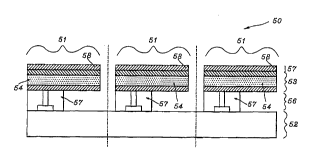
In Fig. 2, there is illustrated a cross sectional
view of a first.f~mho~i nt of an array 50 of M x N thin
film actuated mirrors 51, comprising an active matrix 52,
an array 53 of M x N thin film actuating structures 5~,
an array 55 of M x N supporting members 56 and an array 57
of M x N mirrors 58.
WO9S/12287 2i7~ r~"~ ~ tl48
-- 7 --
Fig. 3 represents a detailed cross sectional view of
a thin film actuated mirror 51 shown in Fig. 2. The
nctive matrix 52 ineludes a substrate 59, an array o~ M
x N transistors (not shown) and an array 60 of M x N
5 connecting t~rmint~l c 61. ISach of the thin film actuating
structures 54 is provided with a top and a bottom surfaces
61, 63, a proximal and a distal ends, 64, 65, and further
includes at least a thin film layer 66 of a motion
;nrqllc3ns material having a top and a bottom surfaces 67,
68 and a first and second electrodes 69, 70 of a specific
~h;Ln~c5, made of, e.g., a metal such as gold (Au) or
silver (Ag), the first eleetrode 69 having a top surface
39. The first electrode 69 is placed on the top surface
67 of the motion-inducing thin film layer 66 and the
second electrode 70, on the bottom surface 68 thereof.
The motion-;ndl~in~ thin film layer 66 is made of a
piezoelectric ceramic, an electrostrictive ceramic, a
magnetrostrictive ceramic or a piezoelectric polymer. In
the case when the motion-in~ ;nq thin film layer is made
20 of a piezoelectric ceramie or a piezoeleetric polymer, it
must be poled.
Each of the M x N fiupporting members 56, provided
witll a top and bottom surfaces 71, 72, is used for holding
each of the actuating structures 54 in place and also for
25 electr -lly connecting the second electrode 70 in each of
the a ~ating strllctures 54 with the corresponding
connecting termina -= 61 on the active matrix 52 by being
provided with a ct~nduit 73 made of an electrically
conductive material , e . g ., a metal . In this inventive
30 array 50 of M x N thin film actuated mirrors 51, each of
the actuating structures 54 is cantilevered ~rom each of
the supporting members 56 by being mounted on the top
surface 71 of each of the supporting r~mbers 56 at the
bottom surface 63 of each of the actut _ng structures 54
35 at the proximal end 64 thereof, ~nd trA~ bottom surface 72
WO g5/12287 r~ 48
~.15lq~ 0
-- 8 --
of each of the supporting members 56 is placed on top of
the active matrix 52. Each of the M x N mirrors 58 for
reflecting light beams is placed on top of each of the
actuating structures 54. An electrical field is
applied across the motion-;nA~c;n~ thin film layer 66
between the first and second electrodes 69, 70 in each of
the actuating structures 54. The application of such an
electric field will cause a deformation of the motion-
inc~llrin~ layer 66, hence the actuating structure 54, and
hence the mirror 58 placed on top thereof.
In order f or the array 50 of M x N thin f ilm actuated
mirrors 51 to function properly, the combined ~h;~kn~55 Of
the mirror 58 and the first electrode 69 in each of the
thin film actuated mirrors 51 must be different from that
of the second electrode therein for the deformation
thereof to take place.
If not, an elastic layer 88 having a top surface 40 must
be further provided to each of the actuated mirrors 51.
The elastic layer 88 can be placed either inte ';~te the
mirror 58 and the first electrode 69 or on bottom of the
second electrode 70 in each of the actuated mirrors 51, as
illustrated in Figs. 4 and 5.
The electrically conducting material making up the
first electrode 69 can be also light reflecting, e.g.,
aluminum (Al), which will allow the top surface 39 of the
first electrode function also as the mirror 58 in each of
the thin film actuated mirrors 51. In such a case, in
order for each of the thin film actuated mirrors 51 to
function properly, the first and the second electrodes 69,
70 must be of a different ~h;~kn~-ss or each of the thin
film actuated mirrors 51 must be provided with an elastic
layer 88 placed on the bottom surface of each of the
actuating structures therein, as shown in Figs. 6 and 7.
Furthermore, if the elastic layer 88 is made of a light
re~lecting material, it can also function as the mirror
WO~5/12287 2 1 75 1 9~ 1 11 1t 148
.
_ g _
58, as depicted in Fig. 8.
It is possible for the inventive array S0 of thin
film actuated mirrors 51 to function equally well by
having the top and bottom surfaces 67, 68 of the motion-
inr3~ in~ thin film layer 66 in each of the actuating
xtructures 54 covered completely with the first and second
electrodes 69, 70 or by having either one of the top and
bottom surfaces 69, 7~ of the motion-;n~l~rin~ thin film
layer 66 in each of .~e actuating structures 54 covered
partially with the first and second electrodes 69, 70.
Two examples of the actuated mirror 51 having such a
structure are illustrated in Figs. 9A and 9B.
By way of example of the first embodiment, there are
illustrated is Figs. 8 and 10 an array 50 of M x N thin
film actuated mirrors 51 comprising an array of 11 x N
actuating structures 54, made of a pi~ -oelectric ceramic,
e.g., lead zirconium titanate(PZT). ..~ electric field is
applied across the motion-inducing thin film piezoelectric
layer 66 located between the first and second electrodes
69, 70 in each of the actuating structures 54. The
application of the electric field will either cause the
piezoelectric ceramic to contract or expand, ~iep~n-i;n~ on
the polarity of the electric field with respect to the
poling of the piezoelectric material. If the polarity of
the electric field ~rresponds to the polarity of the
piezoelectric c.~LL~:~o.lds to the polarity of the
piezoelectric ceramic, the piezoelectric ceramic will
contract. If the polarity of the electric field is
opposite the polarity of the piezoelectric ceramic, the
piezoelectric ceramic will expand.
With reference to Figs. 8 and lO the polarity of the
piezoelectric ceramic corresponds to the polarity of the
applied electric field, causing the piezoelectric ceramic
to contract.
3e~ :use the elastLc layer 88 doe~ :ot oon'cract, th~
WO 95/12287 2 1 7 5 1 9 8 P~ ~ l48
O
-- 10 --
actuating structure bends downward, as shown in Fig. lO~
Referring now to Figs. 8 and lO, it can be shown that the
light impinging the top surface 40 of the elastic layer
88, functioning as the mirror 58, of the actuated mirror
5 51 shown in Fig. lO is deflected at a larger angle than
the light reflected from of the unactuated actuated mirror
51 shown in Fig. 8.
Alternatively, an electric field of a revers~
polarity may be applied across the motion-;n~ in~ thin
film piezoelectric layer 66, causing the piezoelectric
ceramic to expand. In this eYample, the elastic layer 88
does not expand, and as a result, the actuating structure
54 bends upward(not shown). ~he light impinging the
mirror 58 of the upwardly actuated mirror 51 is deflected
at a smaller angle than the light deflected from the top
surface ~O of the elastic layer 88 of the unactuated
actuated mirror 51 shown in Fig. 8.
~here is shown in Fig. 11, a cross sectional view of
a second Dmho~i t of an array lOO of M x N thin film
actuated mirrors lOl, wherein the second Dmho~i nt is
similar to the first ~.mho~;- t except that each of the
actuating structures 54 is of a bimorph structure,
including a first electrode 69, a second electrode 70, an
intP ~ te metaL layers 87 an upper motion-inducing thin
film layer 89 having a top and a bottom surfaces 9O, 91
and a lower motion-indl~rin~ thin film layer 92 provided
with a top and bottom surfaces 93, 9~. In each of the
actuating structures 54, the upper and lower motion-
inducing thin film layers 89,92 are separated by the
intD ~ te metal layer 87, the first electrode 69 placed
on the top surface 90 of the upper m.otion-;nCl-l-;n~ thin
film layer 89, and the second electrode 70, on the bottom
surface 9~ of the lower motion-;n~ tc;n~ thin film layer
92 .
35 As in the case of the first ~ --t~ the upper and
WOg~/12287 ;~ 1 7 ~ 48
lower motion-inducing thin film layers 89, 92 in each of
the actuating structures 5~ are made of a piezoelectric
ceramic, an electrostrictive ceramic, a magnetostrictive
ceramic or a piezoelectric polymer. In the case when the
upper and lower motion-;ndl~cin~ thin film layers 89,92 are
made of a piezoelectric ceramic or a piezoelectric
polymer, the upper and lower mo~ion-indll~ing thin film
layers 89,92 must be poled in such a way that the
polarization direction of piezoelectric material in the
upper motion-;n~ rin~ thin film layer 89 is opposite from
that of the lower motion-in/i~cin~ thin film layer 92.
Fig. 12 illustrates a cross sectional view of an actuated
mirror lO1 of the second: ' ~i t, wherein the first
electrode 69 is made of a light reflecting material,
thereby allowing the top surface 39 thereo to also
function as the mirror 58.
As an example of how the second ~-mhQ~i nt functions,
assume that the upper and lower motion-inducing layers 89,
90 in the array 100 of M x N thin film actuated mirrors
101 shown in Fig. ll are made of a piezoelectric ceramic,
e.g., PZT. When an electric field is applied across each
of the actuating structure 54, the upper and lower motion-
inducing thin film piezoelectric layers 89, 92, thc
actuating structure 54 will either bend upward or
downward, depending on the poling of the piezoelectric
ceramic and the polarity of the electric field. For
example, of the polarity causes the upper motion-in~ i
thin film piezoelectric layer 89 to contract, and the
lower motion-inducing thin film piezoelectric layer 92 to
expand, the actuating structure 54 will bend upward. In
this situation, the impinging light is deflected of a
smaller angle from the actuating structure 54 than the
deflected light from the unactuated actuating structure
54. However if the polarity of the piezoelectric ceramic
and the electric field causes the upper motion-inc7~ in~
WO95/12287 2 1 7 5 1 9 8 1 ~1,~. . 148
-- 12 --
thin film piezoelectric layer 89 to expand and the lower
motion-inducing thin film piezoelectric layer 92 to
contract, the actuating structure 54 will bend downward.
In this situation, the impinging light is deflected at a
5 lsrger angle f rom the actuating structure 54 than the
def lected light f rom the unactuated actuating structure
54 .
There are illustrated in Figs. 13A to 13F
manufacturing steps involved in manufacturing of the first
~mho~; L of the present invention. The process for
manufacturing the first f~mhotl; t, i.e., the array 50 of
M x N thin film actuated mirror 51, wherein M x N are
integers, begins with the preparation of the active matrix
52, having a top and a bottom surfaces 75, 76, comprising
15 the substrate 59, the array of M x N transistors (not
shown) and the array 60 of M x N connecting t~rm;n:~l c 61,
as illustrated in Fig. 13A.
In the subsequent step, there is formed on the top
surface 75 of the active matrix 52 a supporting layer 80,
20 including an array 81 of M x N pedestals 82 corresponding
to the array 55 of M x N supporting members 56 and a
sacrificial area 83, wherein the supporting layer 80 is
formed hy: depositing a s~rr;f;r;~l layer (not shown) on
the entirety of the top surface 75 of the active matrix
25 52; forming an array of M x N empty slots (not shown), to
thereby generated the sacrificial area 83, each of the
empty slots being located around each of the M x N
connecting t~rm;n~l c 61; and providing a pedestal 82 in
each of the empty slots, as shown in Fig. 13B. The
30 sacrificial layer is formed by using a sputtering method,
the array of empty slots, using an etching method, and the
pedestals, using a sputtering or a chemical vapor
deposition(CVD) method, followed by an etching method.
The sacrificial area 83 of the supporting layer 80 is then
35 treated so as to be removable later using an etching
WO9S/12287 2 t ~ ~ t~ ~ ~ r~l,~s L't ~148
-- 13 --
method or the application of chemicals.
A conduit 73 for electrically connecting each of the
connecting tr~rm;nAl c 61 with each of the second electrode
70, made of an electrically conductive material, e . g .,
s tungsten(~t), is formed in each of the pedestals 82 by
first creating a hole extending from top thereof to top of
the corresponding connecting t~ nr~l s 61 using an etching
method, followed by filling therein with the electrically
conducting material, as depicted in Fig. 13 (c) .
In the subsequent step, as depicted in Fig. 13D, a
first thin film electrode layer 84, made of an
electrically conducting material, e.g., Au, is deposited
on the supporting layer 80. Thereafter, a thin film
motion-;n~ rinrJ layer 85, made of a motion-inducing
material, e.g., PZT, and a second thin film electrode
layer 95 are then respectively formed on the first thin
film electrode layer 84.
Subsequently, a thin film layer 99 of a light
reflecting material, e.g., Al, is provided on top of the
second electrode layer 95.
The thin film layers of the electrically conducting,
the motion-indnrin~J, and the light reflecting materials
may be deposited and patterned with the known thin film
techniques, such as sputtering, sol-gel, evaporation,
etching and micro ~-rhininrJ, as shown in Fig. 13E.
The sacrificial area 83 of the supporting layer 80 is
then removed or dissolved by the application of chemical
to thereby form said array 50 of M x N thin film actuated
mirrors 51, as illustrated in Fig. 13F.
The second: o~'; L is fabricated in a similar
manner as the first embodiment. The supporting layer i5
applied to the active matrix. The supporting layer also
includes the array of M x N pedestals corresponding to the
array of M x N supporting members and the sacrificial
35 area. The first thin film electrode layer, the lower thin
WO 95/12287 ~ 148
~7~t~3 0
-- 14 --
film motion-in~ rin~ layer, the int~ te metal layer,
the upper thin film motion-;nd~ n~ layer, the second thin
film electrode layer, and the light reflecting layer are
then deposited respectively on the supporting layer. The
thin film layers of an electrically aonducting, a motion-
;n~ ;ng and a light reflecting materials may be deposited
and patterned with the known thin f ilm techniques, as
stated earlier. The sacrificial area of the supporting
layer is next dissolved or removed by the application of
a r~h~ir~ leaving the array 100 of thin film actuated
mirrors lO1, having the array 53 of M x N actuating
structures 54 with the bimorph structure, each of the
actuating structures 54 being cantilevered f rom each of
the supporting members 56.
~n the above described methods for manufacturing the
first and second ~mho~; Ls of the present invention, an
additional process for forming the elastic layer 88 can be
added, involving a similar process as in the forming of
other thin f ilm layers .
While the present invention has been described with
respect to certain preferred embodiments only, other
modifications and variations may be made without departing
from the scope of the present invention as set forth in
the following claims.