Note: Descriptions are shown in the official language in which they were submitted.
WO 95/14218 PCTIUS94/13002
2175487
INFRARED RADIATION IMAGING ARRAY WITH
COMPOUND SENSORS FORMING EACH PIXEL
BACKGRO 1ND OF THE INVENTION
Quite sensitive and small infrared (IR) sensors which operate on the
principles of
a thermopile are now available. Such sensors provide a small electrical signal
which
varies with the relative strength of the IR radiation impinging on them, and
can be used
to measure the temperature or change in temperature of an object on which a
sensor of
this type is focussed. The most sensitive of these sensors can detect
differences in
to temperature of a few thousandths of a degree Celsius in the object from
which the IR
radiation emanates. Using common photolithographic processes, such sensors can
easily be fabricated in situ in a matrix or array, each sensor forming one of
the pixels in
the array.
It is known that most objects emit amounts and frequencies of infrared
radiation
15 which differ based on the emissivity, angle of the surface to the viewer,
and temperature
of the body itself. The variations in this radiation when allowed to impinge
on an array
of IR sensors produces corresponding differences in the signals from the
individual
sensor elements in the array. The individual signals from the sensors in the
array can
therefore collectively encode an image of the field of view from which the IR
radiation
2o emanates. Typically, the individual output signals from the sensors are
scanned in some
sequential manner to forma composite signal encoding the image and changes in
it in
real time. In this way, such an array can form the IR radiation-sensitive,
image-forming
element of a camera which produces images based on the infrared radiation
emanating
from the field of view. The signal can be used to form a visible image in a
display
25 which accurately represents the spatial relationship of objects in the
field. Such
encoding of an image has been done for many decades in the imaging of visible
light
from a field of view as in television technology.
A recently developed preferred design for IR sensors depending on a
thermoelectric mechanism to provide the signal voltage output, has thin layers
of
3o conductive materials of various types and insulating material which are
deposited in
appropriate patterns on a silicon sensor substrate using well-known
photolithographic
techniques. Thermoelectric junctions are formed by overlapping conductors
during the
WO 95/14218 ~ ~ J r ~. PCT/US94/13002
7 ~~1
deposition. Such sensors will be called hereafter microbridge sensors. The
junctions of
these microbridge sensors are of two kinds, sensor junctions and reference
junctions.
The reference junctions are in close thermal contact with the substrate. Each
sensor
junction is within a small, discrete, area which overlays a pit or depression
formed in the
sensor substrate, and is of an area conforming to the footprint of the sensor
junction. In
cross section, these sensors look much like a bridge spanning a valley, hence
the term
"microbridge". The pits provide a measure of thermal isolation from the
substrate for
their associated sensor junctions. Thus, changing IR radiation impinging on
both the
sensor and reference junctions causes the temperature of the sensor junction
to change
1o more rapidly than does the reference junction, resulting in a temperature
differential
between the junctions which generates a signal. These known photolithographic
techniques allow individual sensors to be easily fabricated in an array so as
to allow
imaging of the IR radiation in a field of view. Leads from the elements
forming the
junctions are led to electronic circuitry which may be formed in layers below
the sensor
substrate. This circuitry scans and amplifies the signals from the individual
sensors to
provide a signal which may be used to reproduce the field of view in a way
analogous to
that of television.
For maximum sensitivity microbridge sensors may be maintained in a low
pressure gas atmosphere or in a vacuum by virtue of reduced heat transfer
between the
2o sensing junction and the substrate, but this requires a hermetically sealed
enclosure
which adds cost and reduces reliability. It is also possible to use a less
tightly sealed
enclosure containing air or other gas at or near atmospheric pressure, at the
cost of less
sensitivity. One should realize that these microbridge sensors are designed to
produce a
usable signal with but a few hundredths or thousandths of a degree Celsius
temperature
differential between the sensing and reference junctions.
One desirable application for these sensors is in arrays for forming images of
relatively low contrast scenes or fields of view, such as may arise indoors in
occupied
rooms. In such fields of view, the inanimate, non-heat producing objects are
all very
nearly at the same temperature. Distinguishing such objects by use of IR
imaging
requires very sensitive sensors. The types of microbridge IR sensors formed
according
to today's technology cannot provide the high quality signals, i.e. resolve
contrasts in
impinging radiation adequately so as to clearly distinguish the typical
variations in IR
2175487
WO 95/14218 PCT/US94/13002
radiation in low contrast fields of view unless the total area of each
individual sensor
pixel is larger than a certain minimum area. Typically, a 6 mil x 6 mil (.15
cm x .15 cm)
or equivalent area is required for vacuum-packaged sensors. Even larger areas
are
required for sensors operating in gas-filled packages. Sensors having such
areas are too
large to reliably fabricate using current processes. In essence, the span
necessary for the
bridge which supports the sensing junction is too great for reliable
fabrication and
adequate resistance to shock and vibration.
BRIEF DESCRIPTION OF THE INVENTION
We have found that the capabilities of large area microbridge sensors can be
duplicated with satisfactory yields by instead using a group of adjacent small
microbridge sensors whose aggregate area is similar to that of a single large
sensor.
Each such group of sensors forms a single pixel for imaging purposes. The
sensitivity
of the device is not reduced significantly by the use of a number of smaller
sensors
15 instead of a single large one of similar area. The small microbridge
sensors in a single
group are connected electrically in series or parallel to form an equivalent
large sensor.
These smaller sensors need span only a small pit which thermally isolates the
sensing
junction, and this can be done with much higher fabrication yields. Further,
if an
occasional smaller sensor is defective, others in a single group will still
provide a signal
2o which can if necessary be enhanced so as to provide at least some
contribution to the
image. This approach allows the individual pixel area to be made as large as
is desired
for adequate sensitivity and resolution. Each sensor may have as few as three
or four
subsensors or as many as thousands.
The small microbridge sensors form in effect a sub-array of sub-sensors which
25 are connected electrically to form a single large area sensor of the
required sensitivity.
Each of the large sensor elements so formed may itself be arranged in an array
of these
larger sensors to allow an image of impinging radiation to be formed.
Such an infrared radiation sensing array comprises a substrate having on a
first
surface, a plurality of pixel areas arranged in an array. Within each pixel
area, a
3o plurality of infrared radiation voltaic microbridge subsensors are arranged
in a sub-array
to comprise a single sensor. Each subsensor has first and second output
terminals across
which appears a voltage responsive to changes in infrared radiation impinging
on the
CA 02175487 2001-12-07
~b4159-1455 (S)
4
subsensor. A plurality of conductors connect the subsensors
of each sensor together in a predetermined manner so as to
provide a composite signal to which each subsensor
contributes. The composite signal from each sensor is
provided on its own conductor to a signal processor. Each
composite signal has the information content that would be
provided by a single large sensor occupying essentially the
same space in the array.
The subsensors comprising a sensor may be
connected in either series or parallel as desired so as to
match the input impedance of the amplifier to which they are
connected. Most conveniently, all of the subsensors forming
a sensor may be arranged in an orthogonal array within the
pixel area and connected in a series arrangement with the
voltage output and internal impedance of each additive to
that of all the others comprising the sensor. To achieve
this, the subsensors in each row of the pixel area array are
connected in series, and the rows of series-connected
subsensors are then connected in series with each other as
well to create a series connection of all of the subsensors
wherein the signal voltages of the sensors are additive.
In accordance with the present invention there is
provided an infrared radiation sensing array comprising a)
substrate (10) having on a first surface, a plurality of
pixel areas arranged in an array; b) within each pixel area,
a sensor (11, 12) comprising a plurality of infrared
sensitive microbridge subsensors (14-17) arranged in a sub-
array, each subsensor (14-17) spanning an underlying pit
(24) and having first and second output terminals across
which appears a voltage responsive to presence of infrared
radiation (45) impinging on a radiation-responsive surface
of the subsensor, at least one of said subsensors (14-17)
within a pixel area having its radiation-responsive surface
CA 02175487 2001-12-07
04159-1455(S)
4a
facing away from the pit (24) within the pixel, said sensor
characterized by, c) within each pixel area, a plurality of
subsensor conductors (26, 38) electrically connecting the
subsensors (14-17) in that pixel area together in a
predetermined manner which provides a composite signal to
which each subsensor contributes electrical energy; and d) a
plurality of sensor output conductors (52, 53), each one
associated with a single sensor (11 or 12), and carrying the
composite signal produced by that sensor (11, 12).
BRIEF DESCRIPTION OF THE DRAWINGS
Fig. 1 is a plan view of an infrared sensor array
built according to the invention of this application.
Fig. 2 is a cross section view of two adjacent
pixel areas from the array of Fig. 1, and is aligned so that
the individual features of Figs. 1 and 2 are vertically
aligned.
Fig. 3 shows an alternative connection between the
subsensors of an infrared radiation sensor array.
DESCRIPTION OF THE PREFERRED EMBODIMENTS
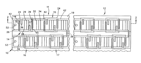
Figs. 1 and 2, which are different views of the
same array device 10, will be described together. In Fig.
1, there are shown two separate pixel areas located at the
upper left hand and upper right hand corners respectively of
a representative infrared imaging array. There may be as
many as several hundred pixel areas in a single row of an
array, and there may be several hundred rows as well in a
high resolution array 10. Each pixel area contains a single
CA 02175487 2001-12-07
x4159-1455(S)
4b
composite sensor 11, 12, etc. formed by photolithographic
processes. The entire array 10 is carried on a base 64,
which typically will be formed of a silicon material and cut
from a larger silicon wafer. The array 10 is
217547
WO 95/14218 PCT/iJS94/13002
formed in and on a thermally conductive heat sink layer 19. It is possible to
form
electrical components and connections beneath heat sink layer 19 within a
group of
contiguous component layers 57 deposited on base 64. The individual components
within component layers 57 if present, as well as the connections between
them, will
s typically also be formed by these well-known photolithographic processes.
These
components and their connections can form circuits for processing the signals
provided
by individual sensors 11, 12, etc.
For exemplary purposes, Figs. 1 and 2 show individual sensors 11 and 12, with
sensor 11 shown as comprising four essentially identical individual subsensors
14-17.
In point of fact sensor 11 may comprise as few as three or four subsensors 14-
17 or as
many as thousands of subsensors. The number of subsensors 14-17 depends on the
sensitivity and resolution required and whether the array 10 is of the vacuum
or gas-
filled type. Each subsensor 14-17 comprises a complete microbridge infrared
sensor
with a sensing junction 47 and a reference junction 50 as is shown for
subsensor 14.
With present technology, each sensor 1 l, 12, etc. may occupy a pixel area
which is on
the order of 6 mils (.15 mm) square. Within each pixel area, the individual
subsensors
14-17 may be arranged in orthogonal rows and columns as shown, although other
spatial
arrangements are possible as well. The subsensors 14-17 are formed and
supported on a
thin layer 42 comprising an electrically insulating material such as
photoresist having
2o relatively good thermal conductivity.
The reference numbers identifying each of the various elements which comprises
each of the subsensors 14-17 have been applied to subsensor 14. Explanation of
the
subsensors forming the device will be with reference to subsensor 14, and
unless
otherwise stated comments with respect to it are true also for each of the
other
subsensors 15-17 comprising sensor 11 and the subsensors comprising sensor 12,
etc.
Subsensor 14 is shown in Fig. 1 as having a cold, or reference junction 50 and
a
hot or sensing junction 47. Reference junction 50 is formed by a first
thermocouple
element 34 which slightly overlaps a second thermocouple element 33 as shown
in Fig.
2, creating intimate electrical contact between them. Each of elements 33 and
34
3o comprise a different conductive material. Sensing junction 47 is formed by
a third
thermocouple element 29 which slightly overlaps a fourth thermocouple element
28 as
shown in Fig. 2, and also creates intimate electrical contact between them.
2i 7431
Thermocouple elements 28 and 34 both comprise a part of layer 26 and are
formed of the same thermocouple material. Thermocouple elements 28 and 3~t
also
serve as first and second output terminals for the signal from each subsensor.
Elements 29 and 33 both comprise a part of layer 32 and are formed of the same
thermocouple material, a material which is different from that forming layer
26. The
material forming layer 32 may be nickel-iron for example, and that forming
layer 26
may be chromium. Other pairs of metals or semiconductors are also known to be
suitable for use as thermocouple elements. However, it is important that they
be
suitable for use in photolithographic or other types of deposition processes
which may
be used in forming these arrays.
Thermocouple layers 26 and ~? and the elements comprising junctions -17 and
~0 are formed on the underlying support layer 42 as a part of the
photolithoaraphic
manufacturing process. Layer :I2 lies un the thicker heat sink substrate layer
19.
Junction ~7 and the portion of support layer 42 underlying junction -17 extend
over a
small cavity, pit, or depression 24 in heat sink layer 19 which provides a
measure of
thermal insulation between junction -17 and layer 19. Layer ~2 adds strength
to the
portion of subsensor 14 overlying cavity 2=1.
The reference junction ~0 of each subsensor 1~-17 is carried on an area of
layer
~.2 which lies directly on and is in close thermal connection with support
layer ~2 and
heat sink layer 19. There is good thermal conductivity between junction ~0 and
heat
sink layer 19, so that when radiation impinges on a subsensor, there will be a
temperature differential between the sensing and reference junctions.
To further increase the temperature differential between the sensing junction
~7 on the
one hand. and the reference junction ~0 and the heat sink layer 19 on the
other, during
fabrication slots 3~ and 36 are formed in layers 26 and =12, and slots 37 and
39 are formed in
layers 32 and :12 adjacent sensing junction -17. For maximum thermal
isolation, It is important
that slots 3~ and 39 each straddle an edge of pit 2-1 as shown. This
arrangement creates
bridges 4=1 and =15 which suspend sensing junction 47 above pit 24 so as to
provide relatively
long heat conduction paths of relatively small cross sectional area between
heat sink layer 19
and sensing junction ~7. There are other equally suitable configurations for
providing thermal
AMENDED SEIEET
2175487
6.1
isolation of sensing junction 47 from heat sink layer 19. It should be
noted that this thermal isolation feature is not the main feature of this
invention.
AMENDED Sa-iEE'f
WO 95/14218
PCT/US94/13002
7
The four subsensors 14-17 comprising sensor 14 are shown in Figs. 1 and 2 in
series connection with layer 26 connecting reference junction 50 of subsensor
14 to
sensing junction 47 of subsensor 15. A bridge 38 forming a part of layer 26
connects
reference junction 50 of subsensor 15 to sensing junction 47 of subsensor 17.
Connectors 52 and 53 form vias passing through layers 42 and 19 to
respectively
connect sensing junction 47 of subsensor 14 and the reference junction of
subsensor 16
to signal processing circuitry within layers 57. Connectors 52 and 53 may
alternatively
be used for connection to external circuitry.
In operation, infrared radiation shown symbolically in Fig. 2 as rays 45
impinges
to on both the sensing and the reference junctions of each of the subsensors
14-21.
Because of the differing thermal conductivities between the sensing junction
47 of a
subsensor 14-17 and heat sink layer 19, and the associated reference junction
50 of the
same subsensor 14-17 and heat sink layer 19, a change in t:he intensity of
infrared
radiation which falls on a sensing junction 47 and its associated reference
junction 50
~ 5 will alter the temperature differential between the two junctions. As
noted above, this
temperature differential is very slight but is sufficient to create a small
signal voltage
between element 28 of subsensor 14 and element 32 of subsensor 16, which
signal
varies as a function of the change in intensity of the infrared radiation
impinging on a
sensor 11, 12, etc. The different temperature differentials within a pixel
area are
2o averaged by the signal resulting from the series connection between the
subsensors 14-
17. Where the changes in intensity of impinging infrared radiation on
different sensors
is different, the resulting voltage signals will also differ allowing an image
of the
infrared radiation pattern to be electronically constructed. In order to be
able to provide
real time images of the infrared radiation pattern, it is important that the
thermal mass of
25 the material suspended above cavities 24 be very small, so that the
temperature of
junction 47 can change very quickly relative to that of junction 50 in
response to
changes in the level of impinging radiation.
Fig. 3 shows a series-parallel connection of four subsensors in each sensor
11,
12, etc. Signal conductor 71 is connected to the connector 38 shown in Figs. 1
and 2,
3o and elements 28 and 34 of respective subsensors 14 and 16 are connected
electrically by
a conductor 70 which may be a part of layers 26 and 32. Connectors 53 and 71
for each
sensor 1 l, 12, etc. then provide to a signal processor 75 the signal
representing the
WO 95/14218 PCT/US94/13002
2175487
changes in intensity of infrared radiation falling on the sensors 1 l, 12,
etc. An
advantage of such an arrangement is that if one of the subsensors should open
electrically or be defectively manufactured, an attenuated signal will still
be provided,
which may then be enhanced if necessary in order to provide a reasonably good
image.
In this way, occasional defects in the subsensors will not result in high
scrap rates for
the complete array. It is also possible to connect all of the subsensors in
parallel to
further reduce the effect of electrically open subsensors. This configuration
will reduce
the internal impedance of the individual sensors.