Note: Descriptions are shown in the official language in which they were submitted.
21'5 X41
1
DIGITAL-TO-ANALOG CONVERTER (DAC) AND METHOD THAT PRODUCE
AN APPROXIMATELY PIECEWISE LINEAR ANALOG WAVEFORM
BACKGROUND OF THE INVENTION
Field of the Invention
The present invention generally relates to digital-to
analog converters (DACs), and more specifically to a DAC
that generates an approximately piecewise linear analog
waveform with reduced spectral distortion and increased
signal-to-quantization-noise ratio (SQNR).
Description of the Related Art
DACs are used to convert a sequence of digital code-
words, where each codeword represents a quantized sample
from an underlying analog waveform, into an analog voltage
or current signal. In digital circuits each bit of the
codeword is represented by a digital signal. In theory,
these signals could be binary weighted, as a function of
the bit's position, and summed together to produce the ana-
log signal. However, the digital signals are only con-
trolled with sufficient accuracy to switch the digital cir-
cuitry, and thus are not precise enough to accurately con-
struct the analog signal. Instead, the digital signals are
used to control electrical switches that switch between
precision limited low and high signal levels. These sig-
nals are binary weighted and summed together to give the
analog signal. As the speed of digital circuitry increas-
es, the slew rate (switching speed) and accuracy of the
switches become increasingly important factors in minimiz-
21'5941
2
ing distortion of the analog signal.
FIG. 1 is a schematic diagram of a conventional DAC 10
that converts a sequence of n-bit binary codewords 12 into
an analog voltage signal Vo. A clock 14 applies a clock
signal 16 to a register 18 so that each codeword is read
out in parallel. Register 18 produces n digital signals
20, one for each bit of codeword 12, that are applied to
respective digitally controlled electrical switches SN_1, Srr-
z,...,So and held for a complete clock cycle. The code-
words' most significant bits (MSBs) are applied to switch
SN_1 and their least significant bits (LSBs) are applied to
switch So .
A reference voltage line -VR and a ground line GND are
selectively applied through digitally controlled electrical
switches SN_1, SN-z. . . . , So to respective binary weighted re
sistors RN_1, RN_z, . . . , Ro. The resistors are connected in
parallel to the inverting terminal 22 of an inverting oper-
ational amplifier (opamp) A1. The opamp's non-inverting
terminal 24 is connected to ground, and a resistor Ro"c is
connected between inverting terminal 22 and opamp output
26. The negative feedback of opamp A1 holds the voltage at
inverting terminal 22 at approximately ground potential.
When the MSB of codeword 12 is high, switch SN_1 con
nects the reference voltage line -VR to resistor RN_1, which
causes a current IN_1 to flow through it. Because the resis
tor values are binary weighted, i . a . RN_1 = R, RN_z = 2R, . . . ,
and Ro = 2"-1R, the currents are related as IN_i = 2IN_z ...
=2N-lIo so that they reflect the significance of their assoc-
iated bits. When the MSB is low, switch SN_1 connects the
ground line to resistor RN_1 so that the voltage drop across
resistor RN_1 is ideally zero, and hence the current IN_1 is
zero. The currents IN_1, . . . , Io are summed at inverting ter
minal 22 to produce a current IS"m that is proportional to
codeword 12 . Isum f lows through Ro"t and generates voltage Vo
at output 26.
21'~~~41
3
Voltage signal Vo is given by:
Vo = ( aN_1 RR +aN_z 2R + . . . +al 2N iR +ao 2r~-1R ) Rouc ( 1 )
where aN_1, . . . , ao are the binary coefficients for the MSB to
the LSB and R is the resistance of RN_1
Factoring equation 1 gives:
V - ( a + 1 a + . . . + 1 a + 1 a VRRouc
o rr-i 2 rr-z 2N_z 1 2N_1 0 ) R ( 2 )
which shows that Vo is proportional to the digital codeword
12 .
As shown in FIG. 2, the ideal voltage signal Vo is a
zero-order-hold (ZOH) or stair-stepped waveform 28 with
infinite slew rate (a discontinuity at the sampling in-
stances) that represents the quantized samples 29 of an
underlying analog waveform 30. The DAC's output voltage
signal Vo is filtered to produce a reconstructed analog
waveform 32 that is a time-shifted approximation of the un-
derlying waveform 30. For DAC 10 to produce an ideal ZOH
waveform 28, the switches SN_1, . . . , So have to switch and set-
tle between the desired plateau levels instantaneously.
However, in practice switches can not switch instantly, and
will overshoot and ring before settling to the plateau lev-
els. Under conventional theory, the accuracy of DAC 10 de-
pends upon how close the switches' actual transfer func-
tions approximate ideal ZOH waveform 28.
As shown in FIG. 3, each switch SN_1, . . . , and So produc
es an output waveform 34 that follows a rising edge 36 at
a finite slew rate, i.e. a non-zero rise time TR1, over
shoots the desired plateau level 38, and rings for a por
tion of the clock period T before settling to plateau level
38. The rise time TR1 is defined as the time it takes for
waveform 34 to rise from 10% to 900 of the difference be-
21"~ ~~~1
4
tween the high and low plateau levels. The slew rate is
the ten-to-ninety percent change in the amplitude divided
by rise time TR1. Settling time TS1 is the time it takes for
waveform 34 to rise from the 10% level and settle to within
a known error bound 40, suitably one-half of an LSB, from
desired plateau level 38. In practice, each switch is de-
signed to approximate an ideal ZOH waveform 42 by minimiz-
ing the settling time TS1.
A well known approach for reducing settling time TSl is
to reduce the switch's rise time TRl. The switch's ringing
is dampened by reducing its parasitic capacitance and in
ductance. However, manufacturing a switch with these char
acteristics is difficult and expensive. Furthermore, even
though the switch's waveform 34 approximates the ZOH wave
form 42 it would be preferable to reduce its spectral dis-
tortion even further.
Kamoto et al. "An 8-bit 2-ns Monolithic DAC," IEEE
Journal of Solid-State Circuits, Vol. 23, No. 1, Feb. 1988,
pp. 142-146 disclose a DAC that reduces the settling time
TSZ of its output waveform 44 (shown in FIG. 3) by control-
ling the switches' rise and fall times. For each codeword
bit, a differential digital signal is applied through a
control driver to a switch that is driven between precision
limited low and high values. The control driver increases
the digital signal's rise time, which has the effect of in-
creasing the switch's rise time TRZ. This suppresses the
ringing and reduces the settling time Tsa-
The control driver is adjusted externally to select
the optimum rise time that minimizes settling time Tsz.
Kamoto shows that when rise time TR2 is too short, ringing
is severe and settling time TSZ is increased. However, if
rise time TRZ is too long settling time TSZ will also be in-
creased, and hence degrade waveform 44. At the optimum
rise time, the countervailing interests of reducing the
rise time and suppressing the ringing are balanced and thus
21"~~~41
provide the minimum settling time. Kamoto discloses opti-
mum rise and fall times of approximately fifteen percent of
the settling time.
Because Kamoto is trying to approximate ZOH waveform
5 42 the rise time, and hence slew rate, must remain rela
tively fast to construct the rising edge of the ZOH wave
form. At these relatively large slew rates, high frequency
parasitic effects cause the waveform's rising edge 46 to be
non-linear. Furthermore, waveform 44 still overshoots the
desired plateau value 38 and rings for a period of time.
The non-linearity of rising edge 46 and the ringing in
waveform 44 cause spectral distortion that would preferably
be reduced.
SUMMARY OF THE INVENTION
The present invention provides a DAC and an associated
conversion method with reduced spectral distortion and in-
creased SQNR.
This is accomplished with a DAC that converts a se
quence of digital codewords into an approximately piecewise
linear analog waveform. The waveform follows rising and
falling edges between plateau levels that approximate the
ideal values of the digital codewords. The DAC processes,
in parallel, each bit of the codewords to produce component
waveforms that are weighted according to their bits' sig-
nificance and summed together to produce the piecewise lin-
ear analog waveform.
Waveform shaping circuits control the rise and fall
times of each component waveform so that the analog wave
form's rising and falling edges settle to within a desired
error bound of a linear output ramp whose slope is a func-
tion of the difference between successive codewords and the
rise or fall times. The rise and fall times are preferably
approximately the same. Limiting switches control the pla-
teau levels of the component waveforms so that the analog
CA 02175941 1999-03-23
6
waveform settles to within the desired error bound of the ideal values
represented by
the codewords. The linear operating region of the limiting switches is
expanded to
maintain the linearity of the rising and falling edges established by the
waveform
shaping circuits.
Accordingly, in one aspect of the present invention there is provided a
digital
to-analog converter (DAC), comprising:
a plurality of waveform shaping circuits that produce drive signals that
switch
during rise and fall times along rising and falling edges, respectively,
between low
and high plateaus in response to a sequence of n-bit codewords in which each
bit
to controls a digital signal that is applied to one: of the waveform shaping
circuits for a
known clock period;
a plurality of limiting switches having transfer functions that limit the
drive
signals' low and high plateau values to low and high limiting values,
respectively,
while approximately maintaining the shape of the rising and falling edges;
~ 5 a weighting circuit that weights the drive signals in accordance with
their
respective bits' positions in the codewords to produce weighted drive signals;
and
a summation circuit that sums the weighted drive signals to construct an
analog waveform having output plateau value:. and rising and falling output
edges,
said waveform shaping circuits setting said rise and fall times so that the
rising
2o and falling output edges settle in rise and fall settling times T~S and
Tfs, respectively,
measured from successive clock edges of said digital signal to within a first
error
bound of a linear output ramp whose slope i.s a function of the difference
between
successive codewords, and said limiting switches setting the low and high
limiting
values so that the output plateau values settle in a settling time TPS
measured from the
25 end of said rise and fall times to within a second error bound of ideal
values
represented by the codewords so that the analog waveform more closely
approximates
a piecewise linear waveform, which has non-zero rise and fall times, than it
does a
zero-order-hold (ZOH) waveform to reduce spectral distortion in the analog
waveform.
3o In another aspect of the present invention there is provided a digital-to
analog converter (DAC), comprising:
CA 02175941 1999-03-23
6a
a plurality of waveform shaping circuits that produce drive signals that
switch
symmetrically along rising and falling edges during transition times between
low and
high plateaus in response to a sequence of n-bit codewords in which each bit
controls
a digital signal that is applied to one of the waveform shaping circuits for a
known
clock period;
a plurality of limiting switches having; transfer functions that limit the
drive
signals' low and high plateau values to low and high limiting values,
respectively,
while approximately maintaining the shape of the rising and falling edges;
a weighting circuit that weights the drive signals in accordance with their
to respective bits' positions in the codewords to produce weighted drive
signals; and
a summation circuit that sums the vveighted drive signals to construct an
analog waveform having output plateau values that settle in settling times TS
and TPS
measured from successive clock edges of said digital signal and the end of
said
transition time, respectively, to within a known error bound of ideal values
represented by the codewords and having rising and falling output edges that
settle in
rise and fall settling times Trs and Tfs, respec~~tively, measured from
successive clock
edges of said digital signal to within said known error bound of a linear
output ramp
whose slope is a function of the difference bet~,veen successive codewords,
said waveform shaping circuits setting the transition time to reduce the sum
of
settling times TPS and TES and the sum of thc: settling times Tps and Tfs so
that the
analog waveform approximates a piecewise linear analog waveform having non-
zero
rise and fall times over a substantial portion of the clock period to reduce
spectral
distortion in the analog waveform while allowing the settling time TS to
increase
thereby reducing the shaping circuits' switchings speed.
In yet another aspect of the present invention there is provided a method for
constructing an analog waveform from a sequence of digital codewords in which
each
bit in the codeword controls a digital signal having a known clock period,
comprising:
producing a plurality of drive signals that switch during rise and fall times
along rising and falling edges, respectively, between low and high plateaus in
3o response to respective digital signals;
CA 02175941 1999-03-23
6b
adjusting the drive signals' low and high plateaus to low and high limiting
values, respectively, as a function of a limiting signal while approximately
maintaining the shape of the rising and falling edges;
weighting the drive signals in accordance with their respective bits positions
in
the codewords;
summing the weighted drive signals to construct an analog waveform having
output plateau values and rising and falling output edges that approximate a
zero-
order-hold (ZOH) waveform, said ZOH waveform having a frequency response for
transferring power from the digital signals to the analog waveform;
1o trimming said rise and fall times so l:hat the rising and falling output
edges
settle in rise and fall settling times T~S and 'Tfs, respectively, to within a
first error
bound of a linear output ramp whose slope :is a function of the difference
between
successive codewords; and
trimming said limiting signal so that the output plateau values settle in a
settling time Tps to within a second error bound of ideal values represented
by the
codewords such that said analog waveform more closely approximates a piecewise
linear analog waveform having non-zero rise and fall times than it does said
ZOH
waveform to reduce spectral distortion in said analog waveform even though
said
piecewise linear analog waveform has a frequency response that transfers power
less
2o efficiently than said ZOH waveform.
In still yet a further aspect of the present invention there is provided a
method
of converting a digital signal that changes at a predetermined clock rate to
an analog
format, comprising, for each successive clock :period:
generating a progressively more lineaa° analog ramp signal that ramps
over a
time period less than a full clock period from approximately the value of the
digital
signal for the immediately preceding clock period to approximately the value
of the
digital signal for the current clock period and converges to a linear output
ramp whose
slope is a function of the difference between the digital signal's values for
the
immediately preceding and current clock periods; and
limiting said analog ramp signal ovc;r the remainder of said clock period
duration to a progressively more linear steady state signal that converges
toward the
value of the digital signal for the current clod: period so that said analog
ramp signal
CA 02175941 1999-03-23
6c
more closely approximates a piecewis;e linear waveform having non-zero rise
and fall times over said clock period than it does a zero-order-hold (ZOH)
waveform
to reduce spectral distortion in the analog ramp signal.
For a better understanding of the invention, and to show how the same may be
carried into effect, reference will now be; made, by way of example, to the
accompanying drawings.
ERTEF DESCRIPTION OF THE D AWTN('~~
FIG. 1, described above, is a schematic; diagram of a known DAC;
1o FIG. 2, described above, is a plot of an analog waveform and the ideal
stair-
stepped output of the DAC shown in FIG. 1;
FIG. 3, described above, is a plot of the rising edge and plateau for a ZOH
waveform for two known DACS;
FIG. 4 is a plot of an approximately piecewise linear analog waveform in
accordance with the present invention;
FIG. 5 is a plot of the frequency response and spectral envelopes for the ZOH
and first order hold (FOH) waveforms;
FIG. 6 is a plot of the DAC's analog output voltage signal;
FIG. 7 is a block diagram of the wavef~rm shaping circuit shown in FIG. 7;
2o FIG. 8 is a schematic diagram of the v~raveform shaping circuit shown in
FIG.
7;
FIG. 9 is a schematic diagram of the limiting switch shown in FIG. 7;
FIG. 10 is a plot of the output voltage versus the input voltage for the
limiting
switch shown in FIG. 9;
FIG. 11 is a schematic diagram of a preferred embodiment of the weighting
and current summing circuit shown in
217594.
7
FIG. 7; and
FIG. 12 is a block diagram of a preferred embodiment
of the DAC shown in FIG. 7.
DETAILED DESCRIPTION OF THE INVENTION
The applicant has found that the frequency response
and SQNR of a DAC can be improved by designing it to pro-
duce an analog voltage signal that approximates a piecewise
linear analog waveform 50, as shown in FIG. 4, instead of
a ZOH waveform 52. Alternatively, the DAC could output an
analog current signal. Piecewise linear waveform 50 is
composed of linear ramps 56 that connect plateaus 58, which
correspond to the values of successive quantized samples 60
from an underlying analog waveform 62. The preferred
waveform 50 has equal rise and fall times, designated Tslew.
Thus, the slope (slew rate) of each linear ramp is the ra-
tio of the difference between successive plateaus 58 and
slew time Tsiew. As shown, T9ler is 50% of the clock period
T. As Tslew goes to zero percent, the piecewise linear wave-
form converges to ZOH wave form 52. Conversely, as Tslew goes
to 100%, waveform 50 converges to a first-order-hold (FOH)
waveform 64.
FIG. 5 plots a DAC's frequency response 66 where the
underlying waveform 62 (in FIG. 4) is a sinewave of fre-
quency fo. The envelope 68 of a DAC's frequency response 66
sin (nF )
varies from r for ZOH waveform 52 to ( sl ~(F Fz) ) 2
n F=
for FOH waveform 64, where Fr is a ratio of output frequency
to clock frequency. Thus, in theory the piecewise linear
waveform 50 is suboptimal when compared to ZOH waveform 52
because its frequency response rolls off faster, which
means it will transfer less power to the output at any giv-
en frequency than the ZOH waveform.
Frequency response 66 includes a desired component 70
at the sinewave frequency and spurs 72 that represent the
2175 X41
8
distortion in the analog voltage signal produced by the
DAC. Spurs 72 will always exist due to quantization noise
incurred when sampling analog waveform 62. However, if the
DAC's analog output voltage signal exactly matches the ZOH
or piecewise linear waveforms, spurs 72 will be approxi-
mately 6 dB per bit less than component 70.
Following this theory, prior DACs generate voltage
signals that try to approximate ZOH waveform 52 as closely
as possible. However, in practice the applicant has found
that by sacrificing some power efficiency a DAC can be de-
signed and controlled to produce an analog voltage signal
that approximates the piecewise linear waveform 50 better
than prior DACs can approximate ZOH waveform 52. This re-
duces the magnitude of spurs 72 and hence improves the
DAC's spectral distortion characteristics and SQNR.
As shown in FIG. 6, a DAC embodying the present inven-
tion generates an analog output voltage signal 74 that
closely follows the approximately piecewise linear waveform
50. Voltage signal 74 has rising and falling edges 76 and
78 that settle to within a desired error bound 80 (suitably
one-half an LSB) of linear ramps 56, and plateaus 82 that
settle to within the desired error bound of plateaus 58.
The rise and fall settling times Trs and TEs are measured
from the beginning of each clock cycle and the plateau set-
tling time TPS is measured from the end of slew time Tslew~
The settling time Ts is measured from the beginning of each
clock cycle to the point where plateau 82 settles to within
the error bound. whereas prior DACs only settle once to
the desired plateau level, voltage signal 74 settles twice
during each clock period to piecewise linear waveform 50.
This increases the amount of time that voltage signal 74
accurately represents the desired waveform 50, which re-
sults in lower distortion and increased SQNR. Thus, dis-
tortion is reduced by reducing the sums TP9 + Trg and Tps + Tfs
so that they are less than a desired portion of the clock
21'~5~~1
9
period, e.g. 50%.
The settling times Tr9, Tf9 and TPs are reduced by in-
creasing the slew time Tslew. This reduces the slew rate,
which reduces the amount of overshoot and suppresses ring-
s ing. Also, a lower slew rate reduces the high frequency
content of rising and falling edges 76 and 78 so that para-
sitic effects are reduced and the edges converge to linear
ramps 56. At a 100% slew rate the settling times would be
minimized, but voltage signal 74 would at most obtain the
desired plateau for an instant at the end o'f each clock
period. If voltage signal 74 is skewed, it may never reach
the desired value. For this reason, and because the enve-
lope of the frequency response rolls off as TsleW is in-
creased, T9le" is preferably set to between approximately 25s
and 90s of settling time T9 to reduce the distortion in
voltage signal 74 while maintaining adequate power effi-
ciency. At clock rates in the GHz range such as found in
data conversion applications, T9=T. At low clock rates in
the KHz range such as in audio applications or in the MHz
range such as in video systems, T9<T. It is not known
whether reducing T9lew to this extent will increase the set-
tling time as measured in the prior DACs.
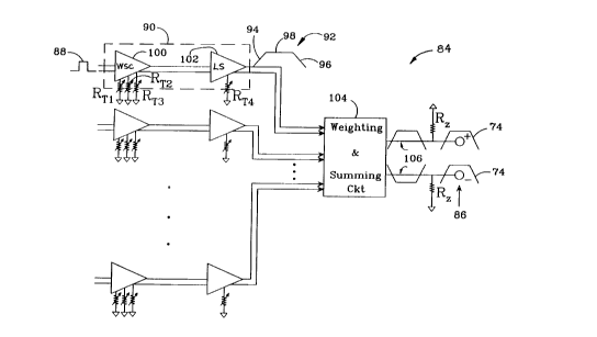
FIG. 7 is a block diagram of a DAC 84 that produces
the approximately piecewise linear voltage signal 74 at a
differential output 86 in response to a sequence of n-bit
digital codewords. Each codeword is represented by n digi-
tal signals 88 that are applied differentially to respec-
tive signal paths 90. The codewords can be binary, ther-
mometer codes, or a hybrid binary/thermometer code. A
thermometer code is formed by mapping an r-bit binary code
into an n=2r-1 bit code where the bits are equally weighted
and turn on cumulatively like a thermometer. A thermometer
code improves the accuracy of the DAC because the output
signals from the signal paths can be summed together with-
out binary weighting. However, a thermometer code requires
CA 02175941 1999-03-23
- 10 ..
substantially more circuitry. Thus, a hybrid binary/thermometer code that
codes the
MSBs with a thermometer code and the LSBs. with a binary may be preferred.
Signal paths 90 generate approximately piecewise linear voltage
signals 92 having rising and falling edges 94 and 96, respectively, that
settle to within
a desired error bound from a linear ramp, and having plateaus 98 that settle
to within
the error bound from an ideal value represented by that path's associated bit.
Each
signal path 90 includes a waveform shaping circuit (WSC) 100 that controls the
symmetry and slew time TsieW of rising and fal'.ling edges 94 and 96. A
limiting switch
(LS) 102 precision limits plateaus 98 and maintains the linearity of the
rising and
falling edges by expanding its linear operating; range.
Voltage signals 92 are applied to a weighting and current summing
circuit 104 that converts them into current signals, weights the current
signals as a
function of the corresponding bit's significance, and sums them together to
produce a
differential output current 106. If the digital codeword is a binary code,
circuit 104
includes a resistive network that binary wei~;hts and sums the current
signals. The
resistive network is preferably implemented with the well known R-2R ladder to
improve the accuracy of the DAC. If the codeword is a thermometer code.
voltages
signals 92 are applied across a single resistor to sum the equally weighted
current
signals. A hybrid code uses a portion of the R:-2R ladder (shown in detail in
FIG. 11)
to binary weight the binary LSBs and sum all of the current signals.
Differential
output current 106 flows through a pair of resistors RZ to produce
approximately
piecewise linear voltage signal 74 at differential output 86.
DAC 84 is calibrated by exter;-nally trimming the waveform shaping
circuits 100 and linear switches 102 until the rising and falling edges and
plateaus of
its analog voltage signal 74 settle to ~,vithin the desired error bound 80
21'~~~~1
11
(shown in FIG. 6), are symmetric and have the correct duty
cycle. To improve the accuracy of DAC 84, signal paths 90
are preferably calibrated independently by applying a high
digital signal 88 to one signal path and low digital sig-
pals to all the other paths, and monitoring voltage signal
74. To ensure that the cumulative error is within one-half
of an LSB, the individual waveforms will generally have to
conform to a tighter error bound. One approach is to set
the root-mean-square of the individual error bounds to
equal one-half an LSB. Alternatively, the known differen-
tial and integral error measures can be used.
To calibrate DAC 84, waveform shaping circuits 100
have trimming circuits that are represented by trimming
resistors RT1, RTZ and RT3, and linear switches 102 have a
trimming circuit that is represented by trimming resistor
RTq. Trimming RT1 balances waveform shaping circuit 100 so
that the rise and fall times of voltage signal 92 are sym-
metric. However, this causes voltage signal edges 94 and
96 to shift in time independently and change the signal's
duty cycle. Therefore, the shaping circuits are precomp-
ensated to offset the relative time shift of 94 and 96 by
trimming RT2. Trimming RT3 reduces the rise and fall times
of voltage signal 92 until the rising and falling edges of
the DAC's output voltage signal 74 settle to within the
predetermined error bound from the linear ramp. These re-
sistors are trimmed so that each signal path satisfies the
error bound and preferably the rise and fall times for each
waveform 92 are approximately equal. Trimming resistor RT4
sets the high and low plateau levels to within the prede-
termined error bound from the ideal plateau levels, which
are a function of the corresponding bits significance.
FIG. 8 is a schematic diagram of waveform shaping cir-
cuit 100. Digital voltage signal 88 is applied to a dif
ferential input 118. A level shifting circuit 120 shifts
voltage signal 88 and applies it to the bases 122 and 124
21'~~~41
12
of an emitter-coupled pair 125 of npn transistors Q1 and
Q2, respectively. Collectors 126 and 128 of transistors Q1
and Q2 are respectively connected to a differential output
130, and through bias resistors R~ to a high supply voltage
V~~, suitably ground reference potential. When voltage sig-
nal 88 is high (low), transistor Q1 turns on (off) and Q2
turns off (on) so that the polarity of the voltage signal
131 at differential output 130 is 180° out of phase with
respect to digital voltage signal 88. The high and low
plateau values for voltage signal 131 are limited by the
size of resistors R~, typically 300 to 1K ohms, and the
amount of emitter current Ie, typically 400~,A to 3mA .
The rise and fall times of voltage signal 131 are in
creased by connecting a capacitor C1, suitably 400pF,
across collectors 126 and 128 of transistors Ql and Q2, re
spectively. The size of capacitor C1 can be reduced by ap-
proximately a factor of one hundred by using a Miller mul-
tiplier, which increases the effective capacitance. Capac-
itor C1 resists switching the voltage across differential
output 130, and hence increases the rise and fall times.
The capacitance of C1 and emitter current Ie are selected so
that capacitor C1 charges and discharges between the limit-
ing high and low plateau values in an approximately linear
manner. If the capacitance is too large or the emitter
current too small, the voltage across the capacitor will
increase logarithmically and may never reach the desired
plateau levels before the next clock cycle.
Level shifting circuit 120 comprises four NPN transis
tors Q3 through Q6 whose emitters 132 through 138 are con
nected through biasing resistors Re to a low voltage supply
Vee, suitably -5.2 V. Their collectors 140 through 146 are
connected to the high supply voltage V~~. Differential in-
put 118 is connected to the bases 148 and 150 of transis-
tors Q3 and Q4, respectively. Bases 148 and 150 are tied
through bias resistors Rb to the high voltage supply V~~ to
CA 02175941 1999-03-23
-13-
supply bias current to transistors Q3 and Q4 so that transistors Q3 through Q6
are
always turned on. Emitters 132 and 134 of transistors Q3 and Q4 are connected
to the
bases 152 and 154 of transistors QS and Q6, respectively, and emitters 136 and
138 of
transistors QS and Q6 are connected to bases 122 and 124 of emitter-coupled
transistors Ql and Q2, respectively. This level shifts digital signal 88 down
by two
npn transistor base-emitter voltage drops so that it is compatible with
driving emitter-
coupled pair 125.
A balancing circuit 156 (shovvn as trimming resistor RTl in FIG. 7)
offsets voltage signal 131 to precompensate l:he signal path for the asymmetry
of an
emitter-coupled pair 188 of transistors Q8 and Q9 in limiting switch 102
(shown in
FIG. 9). Transistor Q1's collector current, which remains approximately
constant, is
supplied through its collector resistor R~ and balancing circuit 156.
Balancing circuit
156 supplies and sinks current Ibai from resistor R~ to pull the voltage at
collector 126
up and down, respectively, so that transistors Q8 and Q9 effectively switch at
the
same threshold voltage so that voltage signal 92 is symmetric. Balancing
circuit 156
includes trimming resistors Rbl and R62 that acre connected in series between
the low
and high supply voltages Vee and V~~ at node l~ 58. A resistor Ro is connected
between
collector 126 and node 1 S 8 to provide balancing current Ibai to transistor Q
1.
When the threshold voltage o~f transistor Q8 is higher than that of
transistor Q9, Q8 turns on more slowly and turns off faster than transistor
Q9. To
balance the transistors, resistor R62 is trimmed so that the voltage at node
158 is
higher than the voltage at collector 126. This causes Iba~ to supply a portion
of
transistor Q1's collector current so that the voltage at its collector 126 is
increased.
This causes transistor Q8 to turn on faster and turn off slower. Conversely,
when the
threshold voltage of transistor Q8 is lower than that of transistor Q9,
resistor
_ 217591
14
Rbl is trimmed so that the voltage at node 158 is lower than
the voltage at collector 126. This increases the current
flowing through collector resistor R~ and pulls the voltage
at collector 126 down, which makes Q8 turn on slower and
turn off faster. Resistors Rbl and Rbz are trimmed until the
rise and fall times observed at the output of each signal
path 90 are substantially the same.
Transistors Q1 and Q2 preferably switch between the
same high and low voltage levels at their respective col
lectors. For this to occur, the equivalent resistance at
collectors 126 and 128 must be the same. Therefore, a re-
sistor R1 is connected between the high voltage supply V
and collector 128 of transistor Q2 so that it is in paral-
lel with resistor R~. The resistance of R1 is selected so
that it has the resistance of Ro in series with the parallel
combination of the nominal values for Rbl and Rbz.
Balancing circuit 156 balances emitter-coupled pair
188 but also changes the duty cycle of voltage signal 92.
To maintain synchronism between signal paths 90, a precom
pensation circuit 160 (shown as trimming resistor RTZ in
FIG. 7) shifts one side of the differentially applied digi-
tal voltage signal 88 by increasing or reducing the amount
of base current supplied to base 150 of transistor Q4.
Precompensation circuit 160 includes trimming resistors Rpl
and Rpz that are connected in series between voltage sup-
plies V~~ and Vee at node 162. A resistor Rz is connected
between node 162 and base 150 and a resistor R3 is connected
between base 148 of transistor Q3 and high voltage supply
V~~. The resistance of R3 is selected to be the resistance
of Rz in series with the parallel combination of the nominal
values for RP1 and Rpz . Resistors RPl and RPZ are trimmed to
move the voltage at node 162 above or below the voltage at
base 150 to modify the base current as required to offset
the skew caused by balancing circuit 156.
The symmetric rise and fall times of voltage signal
217 i X41
92, and hence the rise and fall times of the DAC's analog
voltage signal, are set by adjusting the total tail current
Ie drawn from emitters 164 and 166 of emitter-coupled tran-
sistors Q1 and Q2, respectively. When emitter-coupled pair
5 125 switches in response to digital signal 88, the polarity
of tail current Ie switches with respect to capacitor CI so
that it charges or discharges capacitor C1. Reducing tail
current Ie slows the response of capacitor C1 which increas-
es the rise and fall times.
10 To control tail current Ie, emitters 164 and 166 are
connected to the collector 168 of an npn transistor Q7
whose emitter 170 is connected through trimming resistor RTs
to low voltage supply Vee. A reference voltage Vrefl is ap-
plied to the base 172 of transistor Q7 so that it supplies
15 tail current Ie. Resistor RT3 is trimmed until the symmetric
rise and fall times are increased to the point that the
rising and falling edges of the DAC's analog voltage signal
settle to within the desired error bound of the linear
ramp. Furthermore, the resistors RTZ in each signal path 90
are preferably trimmed so that the rise and fall times as
sociated with each signal path are substantially the same.
FIG. 9 is a schematic diagram of limiting switch 102.
Voltage signal 131 is applied to limiting switch 102 at a
differential input 180. A level shifting circuit 182
shifts voltage signal 131 and applies it to the bases 184
and 186 of the emitter-coupled pair 188 of NPN transistors
Q8 and Q9, respectively. Level shifting circuit 182 in-
cludes transistors Q10 through Q13 and respective emitter
biasing resistors Re that are connected in the same manner
as level shifting circuit 120 (shown in FIG. 8).
Emitter-coupled pair 188 produces voltage signal 92
differentially across its collectors 189 and 190 at differ-
ential output 192. The high and low plateau levels of
voltage signal 92 are precision limited by adjusting the
total emitter current Iez supplied by emitter-coupled pair
21~5~41
16
188. This is done by connecting collector 194 of a tran-
sistor Q14 to a common emitter junction 196 between the
emitters 198 and 200 of transistors Q8 and Q9, respective-
ly. Transistor Q14's emitter 202 is connected through the
trimmable resistor RT4 to the low supply voltage Vee, and its
base 204 is connected to a reference voltage Vrefz~ Resistor
RTQ is trimmed until the plateau values for the DAC' s analog
voltage signal are within one-half a LSB of the ideal val-
ues represented by the digital codewords.
To maintain the linearity of the voltagesignal' s ris-
ing and falling edges that was established by the waveform
shaping circuit, the range of input voltages over which
emitter-coupled pair 188 behaves approximately as a linear
amplifier is increased. This can be accomplished in a num-
ber of ways, such as by using emitter degeneration resis-
tors or scaled parallel transistors. As shown, emitter
degeneration resistors Rd, typically less than approximately
100 ohms, are connected between junction 196 and emitters
198 and 200 of transistors Q8 and Q9. As shown in FIG. 10,
this extends the linear range of the emitter coupled pair's
transfer function 204 by an amount approximately equal to
IezRa.
FIG. 11 is a preferred embodiment of weighting and
summing circuit 104 that includes a pair of well known R-2R
ladders 206. Voltage signals 92 from signal paths 90 are
applied differentially to respective nodes 208. As shown,
the codeword is a 12 bit hybrid binary/thermometer code,
which is formed from an 8 bit binary code by mapping its
five LSBs directly into the five LSBs in the hybrid code.
The binary code's 3 MSBs are mapped into 7 equally weighted
bits in the hybrid code. The weight of each of these seven
bits is equivalent to the sixth bit in the binary code.
The equivalent resistance of R-2R ladders 206 at nodes
5 through 11 is R so that the current signals IS through I11,
which correspond to the thermometer coded bits, are equally
CA 02175941 1999-03-23
-17-
weighted. Ladders 206 divide current signal:; I4 - Io so that the proper
binary fraction
of each current signal is provided to the output. The current signals at each
node 208
are summed together to produce differential c;urrent signal 106, which is
proportional
to the digital codewords input to the DAC.
FIG. 12 is a block diagram of a preferred embodiment of DAC 84.
The circuitry of DAC 84 shown in FIG. 7 is expanded to include a recoder 210
that
maps an m bit binary code into a n bit hybrid binary/thermometer code,
calibration
selection circuits (CSC) 212 that allow independent calibration of signal
paths 90, and
latch circuits 214 that resynchronize digital signals 88 before they are
applied to
waveform shaping circuits 100 and linear switches 102.
The m bit binary codeword is split into its m-w MSBs that are mapped
into 2"'-"'-1 equally weighted bits in the hybrid codeword, and its w LSBs
that are
mapped into the w binary weighted LSBs in the hybrid codeword. Thus, DAC 84
has
n signal paths 90 where n = 2m-"'-1 + w. Digital signals 88 corresponding to
the m-w
MSBs of the binary codeword are applied to a recoder 210 that maps them into
the
2"'-W-1 thermometer coded digital signals 88.
The thermometer coded digital signals 88 are input to their respective
calibration selection circuits 212 and to the selection circuit 212 that
corresponds to
the next lower bit. The second input to the I~ISB's selection circuit is
connected to
ground. In normal operation, a selection disable command is applied to an
external
input (TRIM) so that selection circuits 212 pass digital signals 88 through to
their
respective latches 214.
Digital signals 88 that correspond to the w LSBs in the binary
codeword are input to a delay circuit 218 that: delays the application of
those signals
to their respective latches 214 by an amount of time approximately equal to
the delay
caused by recoder 210 and calibration selection cir-
- 21~5!~~1
18
cuits 212.
Recoder 210, selection circuits 212 and delay circuit
218 skew digital signals 88 relative to each other. To
eliminate the skew, digital signals 88 are applied to
latches 214 in each signal path 90. A clock 220 applies a
clock signal to latches 214, which resynchronizes digital
signals 88 and applies them to waveform shaping circuits
100 at the next clock cycle. The clock signal itself may
be skewed by the circuitry. Delays 222 are used to improve
the synchronization, and are adjusted by externally trim-
ming resistors RTS.
As described above, DAC 84 is preferably calibrated by
calibrating each signal path 90 independently. Signal
paths 90 that correspond to the binary code are isolated by
manipulating the codeword to have only a single high bit.
When enabled through the external input (TRIM), calibration
selection circuits 212 isolate one of the signal paths 90
that correspond to the thermometer coded bits. Selection
circuits 212 include logic circuitry that implements the
truth table shown in table 1 below so that only the highest
bit that would be turned on in normal operation is turned
on during calibration. In table 1, the symbol E indicates
an input code AB that is not possible. Alternatively, se-
lections circuits 212 could be removed and voltage signal
74 calibrated by incrementing the digital codewords.
AB
00 O1 11 10
0 0 1 1 E
S
1 0 1 0 E
TABLE 1
While several illustrative embodiments of the inven-
tion have been shown and described, numerous variations and
_ 217591
19
alternate embodiment will occur to those skilled in the
art. For example, pnp transistors could be used instead of
the npn devices shown, and the circuits reconfigured for
biasing between a positive V~~ and grounded Vee. Such varia-
tions and alternate embodiments are contemplated, and can
be made without departing from the spirit and scope of the
invention as defined in the appended claims.