Language selection

Search

Patent 2176010 Summary

Third-party information liability

Some of the information on this Web page has been provided by external sources. The Government of Canada is not responsible for the accuracy, reliability or currency of the information supplied by external sources. Users wishing to rely upon this information should consult directly with the source of the information. Content provided by external sources is not subject to official languages, privacy and accessibility requirements.

Claims and Abstract availability

Any discrepancies in the text and image of the Claims and Abstract are due to differing posting times. Text of the Claims and Abstract are posted:

  • At the time the application is open to public inspection;
  • At the time of issue of the patent (grant).
(12) Patent Application: (11) CA 2176010
(54) English Title: INTEGRATED CIRCUIT SYSTEM FOR ANALOG SIGNAL STORING AND RECOVERY INCORPORATING READ WHILE WRITING VOLTAGE PROGRAM METHOD
(54) French Title: SYSTEME DE CIRCUITS INTEGRES DESTINE AU STOCKAGE ET A L'EXTRACTION DE SIGNAUX ANALOGIQUES IMPLIQUANT UN PROCEDE DE PROGRAMMATION DE TENSION A LECTURE ET ECRITURE SIMULTANEES
Status: Dead
Bibliographic Data
(51) International Patent Classification (IPC):
  • G11C 11/34 (2006.01)
  • G11C 11/56 (2006.01)
  • G11C 27/00 (2006.01)
(72) Inventors :
  • ENGH, LAWRENCE D. (United States of America)
  • BLYTH, TREVOR (United States of America)
(73) Owners :
  • INFORMATION STORAGE DEVICES, INC. (United States of America)
(71) Applicants :
(74) Agent: RICHES, MCKENZIE & HERBERT LLP
(74) Associate agent:
(45) Issued:
(86) PCT Filing Date: 1995-09-13
(87) Open to Public Inspection: 1996-03-21
Availability of licence: N/A
(25) Language of filing: English

Patent Cooperation Treaty (PCT): Yes
(86) PCT Filing Number: PCT/US1995/011590
(87) International Publication Number: WO1996/008823
(85) National Entry: 1996-05-07

(30) Application Priority Data:
Application No. Country/Territory Date
08/306,266 United States of America 1994-09-14

Abstracts

English Abstract


An integrated circuit which operates to
store an input analog signal within an analog
storage device such as an EEPROM (108) is
disclosed. Initially, a target voltage is determined
for applying to the memory cell with the target
voltage set to about 90 % of the input analog
signal voltage. A high voltage ramp (112) is
applied to the memory cell to set the voltage of
the cell to the target voltage. A read operation is
simultaneously performed while the high voltage
ramp is applied to detect the voltage stored on the
cell and to terminate the application of the high
voltage ramp once the target voltage is reached
(104). Thereafter, a normal read operation is
performed on the memory cell to detect the actual
voltage of the cell. The "read-while writing"
operations are performed a predetermined number
of times to achieve programming of the cell.


French Abstract

Circuit intégré permettant de stocker un signal analogique d'entrée dans un dispositif de stockage analogique tel qu'une mémoire EEPROM (108). Une tension cible est tout d'abord déterminée pour être appliquée à la cellule de mémoire, ladite tension cible étant réglée à environ 90 % de la tension du signal analogique d'entrée. Une rampe de tension élevée (112) est appliquée à la cellule de mémoire afin de régler la tension de cette cellule à la tension cible. Une opération de lecture est effectuée simultanément, tandis que la rampe de tension élevée est appliquée, pour détecter la tension de la cellule et interrompre l'application de cette rampe une fois que la tension cible est atteinte (104). Une opération de lecture normale est ensuite effectuée sur la cellule de mémoire pour détecter la tension réelle de la cellule. Ces opérations de lecture et d'écriture simultanées sont effectuées un nombre de fois prédéterminé pour programmer la cellule.

Claims

Note: Claims are shown in the official language in which they were submitted.


- 23 -

CLAIMS:
What is claimed is:
1. A method for storing an input voltage level within an analog
memory storage element, said method comprising the steps of:
applying a voltage ramp signal directly to the analog memory
storage element for increasing a voltage level stored within the storage
element toward the input voltage level while simultaneously reading and
comparing a resulting voltage level within the storage element with the
input voltage level; and
terminating application of the voltage ramp signal to the storage
element before the voltage level stored therein exceeds the input voltage
level.
2. The method of claim 1, wherein the analog memory storage
element is an EEPROM storage element.
3. In an analog memory device, a method for storing a voltage
level within a storage element of said device, said method comprising the
steps of:
a) receiving a voltage level to be stored;
b) determining a target voltage for applying to the storage element
representative of a voltage level less than the received voltage level;
c) applying a voltage ramp signal to the storage element for
increasing an amount of voltage held in the storage element while
simultaneously reading a voltage level of the storage element to
determine whether the voltage level of the storage element matches the
target voltage;


- 24 -
d) deactivating the voltage ramp signal when the voltage level of
the storage element matches the target voltage;
e) reading a resulting stored voltage of the storage element;
f) increasing the target voltage by an amount proportional to a
difference between the resulting stored voltage and the received voltage
level; and
g) repeating steps c) - f) a predetermined number of times.
4. The method of claim 3, wherein the target voltage is initially
chosen to be 90% of the received voltage level.
5. The method of claim 4, wherein, after an initial target
voltage is stored within the storage element, subsequent target voltage
levels are set to a previous target voltage level plus 90% of any remaining
difference between the received voltage level and the resulting voltage
level .
6. The method of claim 3, wherein steps c) - f) are repeated four
to six times.
7. The method of claim 3, wherein a pair of storage elements
are provided for storing the received voltage level as a difference voltage,
wherein steps b) - g) are applied to both of the two elements, and wherein
the method further includes the steps of:
h) comparing a resulting voltage difference between the two
storage elements with the received voltage level to determine any
difference therebetween; and


- 25 -
i) adjusting the voltage stored within one of the two storage
elements by an amount sufficient to decrease any difference between the
received voltage level and the difference voltage between the two storage
cells.
8. The method of claim 7, wherein step i) is performed by
j) selecting one of the two storage elements for receiving an
increased voltage;
k) determining a new voltage level for applying to the selected
storage element;
l) determining a target voltage for applying to the selected storage
element representative of a voltage level less than the new voltage level;
m) applying a voltage ramp signal to the selected storage element
for increasing an amount of voltage held in the selected storage element
while simultaneously reading a voltage level of the selected storage
element to determine whether the voltage level of the selected storage
element exceeds the target voltage;
n) deactivating the voltage ramp signal when the voltage level of
the selected storage element exceeds the target voltage;
o) reading a resulting stored voltage of the selected storage
element;
p) increasing the target voltage by an amount proportional to a
difference between the resulting stored voltage on the selected storage
element and the new voltage level; and
q) repeating steps m) - p) a predetermined number of times.
9. The method of claim 7, wherein step i) is performed by


- 26 -
j) selecting one of the two storage elements for receiving an
increased voltage;
k) determining a new voltage level for applying to the selected
storage element;
l) determining a target voltage for applying to the selected storage
element representative of a voltage level less than the new voltage level;
m) applying a voltage ramp signal to the selected storage element
for increasing an amount of voltage held in the selected storage element
while simultaneously reading a voltage level of the selected storage
element to determine whether the voltage level of the selected storage
element exceeds the target voltage;
n) deactivating the voltage ramp signal when the voltage level of
the selected storage element exceeds the target voltage;
o) reading a resulting stored voltage of the selected storage
element;
p) increasing the target voltage by an amount proportional to a
difference between the resulting stored voltage on the selected storage
element and the new voltage level; and
q) repeating steps m) - p) until the difference between the stored
voltage and the received voltage level is less than a predetermined value.
10. The method of claim 3, further including
an initial step of receiving a digital input signal and converting said
digital input signal to a voltage level to be stored; and
including a subsequent step of reading the resulting stored voltage
of the storage element and converting said storage voltage to a digital
signal.


-27-

11. In an analog memory device, a method for storing a voltage
level within a storage element of said device, said method comprising the
steps of:
a) receiving a voltage level to be stored;
b) determining a target voltage for applying to the storage element
representative of a voltage level less than the received voltage level;
c) applying a voltage ramp signal to the storage element for
increasing an amount of voltage held in the storage element while
simultaneously reading a voltage level of the storage element to
determine whether the voltage level of the storage element matches the
target voltage;
d) deactivating the voltage ramp signal when the voltage level of
the storage element matches the target voltage;
e) reading a resulting stored voltage of the storage element;
f) increasing the target voltage by an amount proportional to a
difference between the resulting stored voltage and the received voltage
level; and
g) repeating steps c) - f) until the difference between the stored
voltage and the received voltage level is less than a predetermined value.
12. An apparatus for storing an input voltage level within an
analog memory storage element, said apparatus comprising:
means for applying a voltage ramp signal directly to said analog
memory storage element for increasing a voltage level stored within the
storage element toward the input voltage level while simultaneously
reading and comparing a resulting voltage level within said analog
memory storage element with the input voltage level; and


- 28 -
means for terminating application of the voltage ramp signal to the
storage element before the voltage level stored therein exceeds the input
voltage level.
13. The apparatus of claim 12, wherein the analog memory
storage element is an EEPROM storage element.
14. An apparatus for storing a voltage level within a storage
element, said apparatus comprises:
a) means for receiving a voltage level to be stored;
b) means for determining a target voltage for applying to the
storage element representative of a voltage level less than the received
voltage level;
c) means for applying a voltage ramp signal to the storage element
for increasing an amount of voltage held in the storage element while
simultaneously reading a voltage level of the storage element to
determine whether the voltage level of the storage element matches the
target voltage;
d) means for deactivating the voltage ramp signal when the voltage
level of the storage element matches the target voltage;
e) means for reading a resulting stored voltage of the storage
element;
f) means for increasing the target voltage by an amount
proportional to a difference between the resulting stored voltage and the
received voltage level; and
g) means for controlling means c) - f) to operate a predetermined
number of times.


- 29 -
15. The apparatus of claim 14, wherein the target voltage is
initially chosen to be 90% of the received voltage level.
16. The apparatus of claim 15, wherein, after an initial target
voltage is stored within the storage element, subsequent target voltage
levels are set to a previous target voltage level plus 90% of any remaining
difference between the input voltage level and the resulting voltage level .
17. The apparatus of claim 14, wherein the means for controlling
controls means c) - f) to operate four to six times.
18. The apparatus of claim 14, wherein a pair of storage
elements are provided for storing the input voltage level as a difference
voltage, wherein means b) - g) operate on both of the two elements, and
wherein the apparatus further includes:
means for comparing a resulting voltage difference between the
two storage elements with the input voltage level to determine any
difference there between; and
means for adjusting the voltage level stored within one of the two
storage elements by an amount sufficient to decrease any difference
between the input voltage level and the difference voltage between the
two storage cells.
19. The apparatus of claim 14, wherein said means for
determining a target voltage for applying to the storage element
comprises an integrator.


- 30 -
20. The apparatus of claim 19, wherein the integrator includes a
switched capacitor and an operational amplifier integrator.
21. The apparatus of claim 19, wherein said integrator sums an
initial target voltage and any subsequently generated difference voltages.
22. The apparatus of claim 14, wherein said means for receiving
the analog voltage signal comprises a track and hold circuit.
23. The apparatus of claim 22, wherein the sample and hold
circuit samples the input analog signal voltage with an offset canceled
switched capacitor and an operational amplifier circuit.
24. The apparatus of claim 14, wherein the means for applying
the voltage ramp to the storage element and for increasing the amount of
voltage held in the storage element comprises:
a comparator receiving the target voltage and for continuously
comparing said target voltage with the voltage level of the storage
element;
a latch receiving a signal from the comparator; and
a high voltage ramp circuit connected to the latch for applying a
continuously increasing voltage signal to said storage element until
deactivated by said latch.
25. The apparatus of claim 24, wherein the comparator includes:
a switched capacitor circuit.


- 31 -
26. The apparatus of claim 24, wherein said storage element is
an EEPROM cell.
27. The apparatus of claim 26, wherein said EEPROM cell
includes:
a first transistor device having a drain connected to said high
voltage ramp circuit, a gate connected to a select input line, and a source;
and
a second transistor device having a drain connected to the source of
said first transistor, a gate connected to a clear input line and a source
connected to an output line, wherein said source of said second transistor
is also connected through a current source to a ground.
28. The apparatus of claim 24 further including
a digital to analog converter for converting an input digital signal
to an analog signal to be stored; and
an analog to digital converter for receiving a stored voltage signal
from said storage element and for converting said analog signal to a
digital signal.
29. An apparatus for storing a voltage level within a storage
element, said apparatus comprising:
a) means for receiving a voltage level to be stored;
b) means for determining a target voltage for applying to the
storage element representative of a voltage level less than the received
voltage level;


-32-

c) means for applying a voltage ramp signal to the storage element
for increasing an amount of voltage held in the storage element while
simultaneously reading a voltage level of the storage element to
determine whether the voltage level of the storage element matches the
target voltage;
d) means for deactivating the voltage ramp signal when the voltage
level of the storage element matches the target voltage;
e) means for reading a resulting stored voltage of the storage
element;
f) means for increasing the target voltage by an amount
proportional to a difference between the resulting stored voltage and the
received voltage level; and
g) means for controlling operation of means c) - f) to operate until
the difference between the stored voltage and the received voltage level is
less than a predetermined value.
30. The apparatus of claim 29, wherein a pair of storage
elements are provided for storing the input voltage level as a difference
voltage, wherein means b) - g) operate on both of the two elements, and
wherein the apparatus further includes:
means for comparing a resulting voltage difference between the
two storage elements with the input voltage level to determine any
difference there between; and
means for adjusting the voltage level stored within one of the two
storage elements by an amount sufficient to decrease any difference
between the input voltage level and the difference voltage between the
two storage cells.


-33-

31. An apparatus for storing a voltage level within a storage
element, said apparatus comprising:
a track and hold circuit for receiving the voltage level to be stored;
an integrator for determining a target voltage for applying to the
storage element representative of a voltage level less than the received
voltage level;
a voltage ramp circuit for applying a voltage ramp signal to the
storage element for increasing an amount of voltage held in the storage
element while simultaneously reading a voltage level of the storage
element to determine whether the voltage of the storage element matches
the target voltage; and
a comparator for deactivating the voltage ramp signal when the
voltage of the storage element matches the target voltage; wherein
said integrator also reads a resulting stored voltage of the storage
element, determines a new target voltage and controls the voltage ramp
circuit and the comparator to apply the new target voltage to the storage
element a predetermined number of times.
32. The apparatus of claim 31, wherein the target voltage is
initially chosen by the integrator to be 90% of the received voltage level.
33. The apparatus of claim 32, wherein, after an initial target
voltage is stored within the storage element, subsequent target voltage
levels are set by the integrator to a previous target voltage level plus 90%
of any remaining difference between the input voltage level and the
resulting voltage level .


- 34 -
34. The apparatus of claim 31, wherein the integrator controls
the comparator and the high voltage ramp to operate four to six times.
35. The apparatus of claim 31, wherein said storage element is
an EEPROM cell.
36. The apparatus of claim 35, wherein said EEPROM cell
includes:
a first transistor device having a drain connected to said high
voltage ramp circuit, a gate connected to a select input line, and a source;
and
a second transistor device having a drain connected to the source of
said first transistor, a gate connected to a clear input line, and a source
connected to an output line, wherein said source of said second transistor
is also connected through a current source to a ground.
37. The apparatus of claim 31, wherein the sample and hold
circuit comprises an offset canceled switched capacitor and an operational
amplifier circuit.
38. The apparatus of claim 31, wherein the integrator includes a
switched capacitor and operational amplifier integrator.
39. The apparatus of claim 31, wherein said integrator sums an
initial target voltage and any subsequently generated difference voltages.


- 35 -
40. The apparatus of claim 31, wherein the comparator includes
a switched capacitor circuit.
41. The apparatus of claim 31 further including
an analog digital converter for converting an input digital signal to
a voltage level to be stored; and
an analog to digital converter for receiving said resulting stored
voltage from said storage element and converting said stored voltage to a
digital signal.
42. An apparatus for storing an analog value as a difference in
voltages between a pair of storage elements, said apparatus comprising:
a first and second storage circuits each having
a sample and hold circuit for receiving a voltage level to be
stored;
an integrator for determining a target voltage for applying to
the storage element representative of a voltage level less than the received
voltage level;
a voltage ramp circuit for applying a voltage ramp signal to
the storage element for increasing an amount of voltage held in the
storage element while simultaneously reading a voltage level of the
storage element to determine whether the voltage of the storage element
exceeds the target voltage;
a comparator for deactivating the voltage ramp signal when
the voltage of the storage element exceeds the target voltage; wherein
said integrator also for reading a resulting stored voltage of
the storage element , determining a new target voltage and controlling the
voltage ramp circuit and the comparator to apply the new target voltage
to the storage element a predetermined number of times; and


-36-

wherein said first and second storage circuits receive first and
second input voltages having a difference representative of the analog
value;
wherein said integrator of said first storage circuit also receives
inputs from said sample and hold circuit and said storage element of said
second storage circuit;
wherein said integrator of said second storage circuit also receives
inputs from said sample and hold circuit and said storage element of said
first storage circuit; and
wherein each of said integrators compares a resulting voltage
difference between the two storage elements with the difference in input
voltage levels to determine any difference therebetween, controls
respective comparators and high voltage circuits to adjust the voltage
stored within the respective storage element by an amount sufficient to
decrease any difference between the difference between the input voltage
levels and the difference voltage between the two storage cells.
43. The apparatus of claim 27, wherein the EEPROM cell further
includes:
a comparator having a first input connected to a normal read line
connected to a source of the first transistor and having a second input
connected to a reference voltage, with an output of the comparator
connected to the clear input line of the second transistor.
44. In an analog storage apparatus having a row of EEPROM
cells, an improvement comprising:
providing a reference EEPROM cell having first and second
transistors connected in series, with a gate of the first transistor connected
to a select input line and a gate of the second transistor connected to a


- 37 -
clear input line;
providing a comparator having first and second inputs with the
first input connected to a source of the first transistor and a second input
connected to a reference voltage line and with an output of the
connected to the gate of the second transistor; and
wherein the gate of the second transistor is connected to gates of
second transistors of each of the EEPROM cells of the row of cells.
45. In an analog storage device having a row of storage cells, an
improvement comprising:
providing a pair of EEPROM cells for storing each of a plurality of
analog values, with a first cell of each pair of cells being a reference cell
and with a second cell of each pair of cells being a storage cell, and with a
clear gate of a transistor of the reference cell being selectively controlled tofor variations in the environment of the cell.
46. The improvement of claim 45, wherein the clear gate is
controlled to compensate for temperature variations.
47. In an analog storage device having rows and columns of
storage cells an improvement comprising:
providing an additional row select transistor to a column group of
cells for isolation of a first plurality of storage cells from a second plurality
of storage cells within a single column group, whereby a total
on a read-while-writing line connected to said cells is decreased.


- 38 -

48. In an analog memory device, a method for storing an analog
signal as a difference voltage between a pair of storage elements of said
device, said method comprising the steps of:
for each of said pair of storage elements
a) receiving a voltage level to be stored;
b) determining a target voltage for applying to the storage
element representative of a voltage level less than the received voltage
level;
c) applying a voltage ramp signal to the storage element for
increasing an amount of voltage held in the storage element while
simultaneously reading a voltage level of the storage element to
determine whether the voltage level of the storage element matches the
target voltage;
d) deactivating the voltage ramp signal when the voltage
level of the storage element matches the target voltage;
e) reading a resulting stored voltage of the storage element;
f) increasing the target voltage by an amount proportional to
a difference between the resulting stored voltage and the received voltage
level; and
g) repeating steps c) - f) a predetermined number of times;
then
h) comparing a resulting voltage difference between the pair
of storage elements with the received voltage level to determine any
difference therebetween; and
i) adjusting the voltage level stored within one of the two
storage elements by an amount sufficient to decrease any difference
between the received voltage level and the difference voltage between the
two storage cells.


- 39 -
49. The method of claim 48, wherein step i) is performed by
j) selecting one of the two storage elements for receiving an
increased voltage;
k) determining a new voltage level for applying to the selected
storage element;
l) determining a target voltage for applying to the selected storage
element representative of a voltage level less than the new voltage level;
m) applying a voltage ramp signal to the selected storage element
for increasing an amount of voltage held in the selected storage element
while simultaneously reading a voltage level of the selected storage
element to determine whether the voltage of the selected storage element
exceeds the target voltage;
n) deactivating the voltage ramp signal when the voltage of the
selected storage element exceeds the target voltage;
o) reading a resulting stored voltage of the selected storage
element;
p) increasing the target voltage by an amount proportional to a
difference between the resulting stored voltage on the selected storage
element and the new voltage level; and
q) repeating steps m) - p) a predetermined number of times.
50. An apparatus for storing an analog signal as a difference
voltage between a pair of storage elements, said apparatus
a) means for receiving a voltage level to be stored;
b) means for determining a target voltage for applying to the
storage element representative of a voltage level less than the received
voltage level;


- 40 -
c) means for applying a voltage ramp signal to each storage
element for increasing an amount of voltage held in the storage element
while simultaneously reading a voltage level of the storage element to
determine whether the voltage level of the storage element matches the
target voltage;
d) means for deactivating the voltage ramp signal when the voltage
level of each storage element matches the target voltage;
e) means for reading a resulting stored voltage of each storage
element;
f) means for increasing the target voltage by an amount
proportional to a difference between the resulting stored voltage and the
received voltage level; and
g) means for controlling means c) - f) to operate a predetermined
number of times on both storage cells;
h) means for comparing a resulting voltage difference between the
two storage elements with the received voltage level to determine any
difference there between; and
i) means for adjusting the voltage stored within one of the two
storage elements by an amount sufficient to decrease any difference
between the received voltage level and the difference voltage between the
two storage cells.
51. A method for storing an input voltage level within a non-
volatile analog memory storage element, said method comprising the
steps of:
applying a voltage ramp signal directly to the analog memory
storage element for increasing a voltage level stored within the storage
element toward the input voltage level while simultaneously reading and
comparing a resulting voltage level within the storage element with the


-41-

input voltage level; and

terminating application of the voltage ramp to the storage element
before the voltage level stored therein exceeds the input voltage level.
52. The method of claim 51, wherein the analog memory storage
element is an EEPROM storage element.
53. In an analog memory device, a method for storing a voltage
level within a non-volatile storage element of said device, said method
comprising the steps of:
a) receiving a voltage level to be stored;
b) determining a target voltage for applying to the storage element
representative of a voltage level less than the received voltage level;
c) applying a voltage ramp signal to the storage element for
increasing an amount of voltage held in the storage element while
simultaneously reading a voltage level of the storage element to
determine whether the voltage level of the storage element matches the
target voltage;
d) deactivating the voltage ramp signal when the voltage level of
the storage element matches the target voltage;
e) reading a resulting stored voltage of the storage element;
f) increasing the target voltage by an amount proportional to a
difference between the resulting stored voltage and the received voltage
level; and
g) repeating steps c) - f) a predetermined number of times.


- 42 -
54. The method of claim 53, wherein the target voltage is
initially chosen to be 90% of the received voltage level.
55. The method of claim 54, wherein, after an initial target
voltage is stored within the storage element, subsequent target voltage
levels are set to a previous target voltage level plus 90% of any remaining
difference between the received voltage level and the resulting voltage
level .
56. The method of claim 53, wherein steps c) - f) are repeated
four to six times.
57. The method of claim 53, wherein a pair of storage elements
are provided for storing the received voltage level as a difference voltage,
wherein steps b) - g) are applied to both of the two elements, and wherein
the method further includes the steps of:
h) comparing a resulting voltage difference between the two
storage elements with the input voltage level to determine any difference
therebetween; and
i) adjusting the voltage stored within one of the two storage
elements by an amount sufficient to decrease any difference between the
receiver voltage level and the difference voltage between the two storage
cells.
58. The method of claim 57, wherein step i) is performed by
j) selecting one of the two storage elements for receiving an
increased voltage;


- 43 -
k) determining a new voltage level for applying to the selected
storage element;
l) determining a target voltage for applying to the selected storage
element representative of a voltage level less than the new voltage level;
m) applying a voltage ramp signal to the selected storage element
for increasing an amount of voltage held in the selected storage element
while simultaneously reading a voltage level of the selected storage
element to determine whether the voltage level of the selected storage
element exceeds the target voltage;
n) deactivating the voltage ramp signal when the voltage level of
the selected storage element exceeds the target voltage;
o) reading a resulting stored voltage of the selected storage
element;
p) increasing the target voltage by an amount proportional to a
difference between the resulting stored voltage on the selected storage
element and the new voltage level; and
q) repeating steps m) - p) a predetermined number of times.
59. The method of claim 57, wherein step i) is performed by
j) selecting one of the two storage elements for receiving an
increased voltage;
k) determining a new voltage level for applying to the selected
storage element;
l) determining a target voltage for applying to the selected storage
element representative of a voltage level less than the new voltage level;
m) applying a voltage ramp signal to the selected storage element
for increasing an amount of voltage held in the selected storage element


-44-

while simultaneously reading a voltage level of the selected storage
element to determine whether the voltage level of the selected storage
element exceeds the target voltage;
n) deactivating the voltage ramp signal when the voltage level of
the selected storage element exceeds the target voltage;
o) reading a resulting stored voltage of the selected storage
element;
p) increasing the target voltage by an amount proportional to a
difference between the resulting stored voltage on the selected storage
element and the new voltage level; and
q) repeating steps m) - p) until the difference between the stored
voltage and the input voltage is less than a predetermined value.
60. The method of claim 53, further including
an initial step of receiving a digital input signal and converting said
digital input signal to a voltage level to be stored; and
including a subsequent step of reading the resulting stored voltage
of the storage element and converting said storage voltage to a digital
signal.
61. In an analog memory device, a method for storing a voltage
level within a non-volatile storage element of said device, said method
comprising the steps of:
a) receiving a voltage level to be stored;
b) determining a target voltage for applying to the storage element
representative of a voltage level less than the received voltage level;


- 45 -
c) applying a voltage ramp signal to the storage element for
increasing an amount of voltage held in the storage element while
simultaneously reading a voltage level of the storage element to
determine whether the voltage level of the storage element matches the
target voltage;
d) deactivating the voltage ramp signal when the voltage level of
the storage element matches the target voltage;
e) reading a resulting stored voltage of the storage element;
f) increasing the target voltage by an amount proportional to a
difference between the resulting stored voltage and the received voltage
level; and
g) repeating steps c) - f) until the difference between the stored
voltage and the received voltage level is less than a predetermined value.
62. An apparatus for storing a voltage level within a non-
volatile storage element, said apparatus comprising:
a) means for receiving a voltage level to be stored;
b) means for determining a target voltage for applying to the
storage element representative of a voltage level less than the received
voltage level;
c) means for applying a voltage ramp signal to the storage element
for increasing an amount of voltage held in the storage element while
simultaneously reading a voltage level of the storage element to
determine whether the voltage level of the storage element matches the
target voltage;
d) means for deactivating the voltage ramp signal when the voltage
level of the storage element matches the target voltage;


- 46 -
e) means for reading a resulting stored voltage of the storage
element;
f) means for increasing the target voltage by an amount
proportional to a difference between the resulting stored voltage and the
received voltage level; and
g) means for controlling operation of means c) - f) to operate until
the difference between the stored voltage and the received voltage level is
less than a predetermined value.
63. The apparatus of claim 62, wherein a pair of storage
elements are provided for storing the received voltage level as a difference
voltage, wherein means b) - g) operate on both of the two elements, and
wherein the apparatus further includes:
means for comparing a resulting voltage difference between the
two storage elements with the received voltage level to determine any
difference there between; and
means for adjusting the voltage level stored within one of the two
storage elements by an amount sufficient to decrease any difference
between the received voltage level and the difference voltage between the
two storage cells.
64. An apparatus for storing a voltage level within a non-
volatile storage element, said apparatus comprising:
a track and hold circuit for receiving the voltage level to be stored;
an integrator for determining a target voltage for applying to the
storage element representative of a voltage level less than the received
voltage level;

- 47 -
a voltage ramp circuit for applying a voltage ramp signal to the
storage element for increasing an amount of voltage held in the storage
element while simultaneously reading a voltage level of the storage
element to determine whether the voltage of the storage element matches
the target voltage; and
a comparator for deactivating the voltage ramp signal when the
voltage of the storage element matches the target voltage; wherein
said integrator also reads a resulting stored voltage of the storage
element, determines a new target voltage and controls the voltage ramp
circuit and the comparator to apply the new target voltage to the storage
element a predetermined number of times.
65. The apparatus of claim 64, wherein the target voltage is
initially chosen by the integrator to be 90% of the received voltage level.
66. The apparatus of claim 65, wherein, after an initial target
voltage is stored within the storage element, subsequent target voltage
levels are set by the integrator to a previous target voltage level plus 90%
of any remaining difference between the input voltage level and the
resulting voltage level.
67. The apparatus of claim 64, wherein the integrator controls
the comparator and the high voltage ramp to operate four to six times.
68. The apparatus of claim 64, wherein said storage element is
an EEPROM cell.

48
69. The apparatus of claim 68, wherein said EEPROM cell
includes:
a first transistor device having a drain connected to said high
voltage ramp circuit, a gate connected to a select input line, and a source;
and
a second transistor device having a drain connected to the source of
said first transistor, a gate connected to a clear input line, and a source
connected to an output line, wherein said source of said second transistor
is also connected through a current source to a ground.
70. The apparatus of claim 64, wherein the sample and hold
circuit comprises an offset canceled switched capacitor and an operational
amplifier circuit.
71. The apparatus of claim 64, wherein the integrator includes a
switched capacitor and operational amplifier integrator.
72. The apparatus of claim 64, wherein said integrator sums an
initial target voltage and any subsequently generated difference voltages.
73. The apparatus of claim 64, wherein the comparator includes
a switched capacitor circuit.
74. The apparatus of claim 64 further including
an analog digital converter for converting an input digital signal to
a voltage level to be stored; and

49
an analog to digital converter for receiving said resulting stored
voltage from said storage element and converting said stored voltage to a
digital signal.
75. An apparatus for storing an analog value as a difference in
voltages between a pair of non-volatile storage elements, said apparatus
comprising:
a first and second storage circuits each having
a sample and hold circuit for receiving a voltage level to be
stored;
an integrator for determining a target voltage for applying to
the storage element representative of a voltage level less than the received
voltage level;
a voltage ramp circuit for applying a voltage ramp signal to
the storage element for increasing an amount of voltage held in the
storage element while simultaneously reading a voltage level of the
storage element to determine whether the voltage of the storage element
exceeds the target voltage;
a comparator for deactivating the voltage ramp signal when
the voltage of the storage element exceeds the target voltage; wherein
said integrator also for reading a resulting stored voltage of
the storage element, determining a new target voltage and controlling the
voltage ramp circuit and the comparator to apply the new target voltage
to the storage element a predetermined number of times; and
wherein said first and second storage circuits receive first and
second input voltages having a difference representative of the analog
value;
wherein said integrator of said first storage circuit also receives
inputs from said sample and hold circuit and said storage element of said


second storage circuit;
wherein said integrator of said second storage circuit also receives
inputs from said sample and hold circuit and said storage element of said
first storage circuit; and
wherein each of said integrators compares a resulting voltage
difference between the two storage elements with the difference in input
voltages to determine any difference therebetween, controls respective
comparators and high voltage circuits to adjust the voltage stored within
the respective storage element by an amount sufficient to decrease any
difference between the difference between the input voltages and the
difference in voltage between the two storage cells.
76. In an analog storage apparatus having a row of non-volatile
cells, an improvement comprising:
providing a reference cell having first and second transistors
connected in series, with a gate of the first transistor connected to a select
input line and a gate of the second transistor connected to a clear input
line;
providing a comparator having first and second inputs with the
first input connected to a source of the first transistor and a second input
connected to a reference voltage line and with an output of the
comparator connected to the gate of the second transistor; and
wherein the gate of the second transistor is connected to gates of
second transistors of each of the cells of the row of cells.
77. An apparatus for storing an analog signal as a difference
voltage between a pair of non-volatile storage elements, said apparatus
comprising:
a) means for receiving a voltage level to be stored;

51
b) means for determining a target voltage for applying to the
storage element representative of a voltage level less than the received
voltage level;
c) means for applying a voltage ramp signal to each storage
element for increasing an amount of voltage held in the storage element
while simultaneously reading a voltage level of the storage element to
determine whether the voltage level of the storage element matches the
target voltage;
d) means for deactivating the voltage ramp signal when the voltage
level of each storage element matches the target voltage;
e) means for reading a resulting stored voltage of each storage
element;
f) means for increasing the target voltage by an amoumt
proportional to a difference between the resulting stored voltage and the
received voltage level; and
g) means for controlling means c) - f) to operate a predetermined
number of times on both storage cells;
h) means for comparing a resulting voltage difference between the
two storage elements with the received voltage level to determine any
difference there between; and
i) means for adjusting the voltage level stored within one of the two
storage elements by an amount sufficient to decrease any difference
between the received voltage level and the difference voltage between the
two storage cells.

Description

Note: Descriptions are shown in the official language in which they were submitted.


217v~1D
WO 96/08823 PCTNS95111590
TNTEGRATET~ ~'TRCUIT SYSTFM FOR ~AI.OG SIGNAT. STORTNG
AND RPCOVT~R~ INCORPORATING 3~T~AT~ W~TTl F WRITING
VOLTAGE p~R~OGRAM ~T~lOD
BACKGROUND OF T~TF INVF~TION
1. Field of th.. Tnvention
The invention generally relates to the field of int~rat~l circuit
analog storage devices and in particular to a method and apparatus for
p.. r~,- u-iL-g voltage program ~ within analog storage cells
thereof.
.


2. D~ yLv-- of R~l ' Art
U.S. Patent No. 4,890,259 discloses a nonvolatile, high-density
i - - l~- ,. 1.-. l circuit analog circuit recording and playback system whereinan analog input signal is sampled a plurality of times and then, as
a~litinn~l samples are being taken and temporarily held, a prior set of
samples of the analog signal are parallel loaded into a plurality of storage
sites, or cells, each ~ liDillg nonvolatile floating gate memory cells,
preferably EEPROM cells. In that system, writing of the groups of
samples into the respective storage cells is performed by i~claLivcly
providing a write pulse followed by a read operation for the respective
cellstocomparethe;.. ~.. ~li.. ~storedmeachcellwiththe;.. r.. ,~li
held by the Ica~e.Livc track and hold circuit. During bU~ CDDiVC
write/read u~ldLiollD, the write pulse is increased m amplitude, with the
write pulses to amy cell being stopped or ~ mlrL~l from the cell, after the

WO 96/08823 ~ PCT/US95111590
e~ -2-
inf rm~ti~n read from the cell m a previous read operation ~ ur ulldiely
equals the value held in the respective track and hold circuit.
U.S. Patent No. 4,989,179 desdbes the use of analog memory m
order to store digital data as mlllti-level analog infnrTn~tl~n. Also
described is an . .. ~;,.. .;,,.I ;~.1 l of the array of analog memory.
U.S. Patent No. 5,126,967 provides an ,~ uluv~ll~ to the system
of U.S. Patent No. 4,890,259 wherein ûne or more ~ d storage
columns are mcluded in the arlay at each side of the storage side array
and are used to store a reference signal at the same time that the adjacent
storage cell stûres a signal sample. During playback, the stored ~ rrr~ `r~ 1
signals are read back and weighted relative to each other m accordance
with the relative column positiûn of the signal storage cell being
~innl~lt~nPnusly read, with the ~utput signal bemg taken as the difference
between the sample signal read back and the reference signal read back
(as weighted relative to each other as per the position m the row of the
signal cell).
U.S. Patent No. 5,241,494 also provides an Ull~lUV~ to the
system of U.S. Patent No. 4,890,259. In the system of U.S. Patent No.
5,241,494, a multi-level iterative write process is provided for achieving
~. uy,. ..~ of the analog storage cells with high-rf~qnl1ltinn. In
particular, a coarse cycle of, . I~ abU Ig vûltage pulses are applied to a cell
being written to quickly set the voltage of the cell to near a target voltage.
The coarse cycle is achieved by t~ ul~y ulg a voltage ramp having a fairly
steeply;,.. ,~ voltage. Duringab,.l,~r,l"r"lfinecycleofrecording,
the stored voltage is fine-tune~ by applying iterative pulses based on a
vûltage ramp having a more gradual voltage increase.
ln each of the foregomg, a read operation is p. rforrn~rl on each
EEPROM cell after each respective voltage pulse is applied to determme
whether the resulting voltage of the EEPROM cell is clûse to or exceeds a
target voltage. If the resulting voltage exceeds the target voltage, the cell
is said to be ûver-~ u~ In the systems described, over-program
can be corrected orlly by ~ul~ ly clearing the over-lulu~,lculul~:d cell
and repeating the entire iterative write process to that cell. To avoid the
.. . .. . .. . _ _ ..

WO 96/08823 il l PCINS95111590
_3_
need to clear a cell and repeat the iterative storage v~ livlLs, slight
amounts of over-program or under-program of the voltage are tolerated,
thus resulting in less resolution than could th~nr~i~ Ally be achieved. It
would be desirable to provide an improved method for progr~mmin~ the
volhge of analog storage cells wherein a higher degree of rPgnllltlnn may
be achieved.
This improved resolution is useful for storage of digital data as
multi-level analog ;..~. ,.,.,~li....
A program method which could operate more quickly by requiring
fewer high voltage write u~.~. ,. l ;~ .. .~ is desirable since a smaller more
economic ~ bodi~ lll results with fewer column driver circuits for the
same sample rate.
When high speed ~. v~ is the system objective, then the
number of high voltage write u~ a~iull~ must be . . .i, .i., .i,~.1
SUMMARY OF TT~F. INVE~TION
In accordance with one aspect of the invention, an improved
method and apparatus for lu, v~ l .. , .. g an analog voltage cell is
provided wherein over-program of each cell is gl-hst~nti~lly avoided, in
part, by reading the analog cell gim~ v~ .~ly while it is being written.
By reading the analog cell while it is being written, potential over-
program of the cell is detected almost i - ~ ;_ l f ly and the write
operationis1 ",.i..~ l beforeanycit,.,;rii,., lover-programoccurs. As
such, a greater degree of resolution may be achieved in accordance with
the invention than is achieved in analog storage systems wherein a
separate read operation is p~, r.., ...f ~1 at the completion of each write
operation. Herein the step of reading the stored voltage as it is being
written is referred to as a "read-while-writing" step.

WO 96108823 ? ~ 6 PCI[IUS95111~90
Inone~ boll~ oftheinvention,theforegoingis ,,~ 1l~IL~d
using a non-volatile analog storage cell as follows. lnitially, an input
analog voltage signal to be stored is received. A tdrget voltage for
applying to the storage element is ~lf '~ based on the input voltdge
with the tdrget voltage set to a level which is somewhat less than the input
voltdge. A high voltdge ramp signal is then applied to the storage element
for increasing the voltage of the storage element. The voltage level of the
storage element is gim~ eu-~ly read to determine whether the voltdge
level exceeds the target voltage and, if so, the voltage ramp is ded~iVd~d.
Thereafter, a normal read operation is performed for redding the volhge
level of the storage element. The tdrget voltage is then increased by an
amount lu~ ul~ al to any rf~m~inin~ difference between the stored
voltage and the input voltage. The steps of applying the high volhge
ramp while ~.. " " 11l ... ,.-l u~ly reading the voltage level and then increasmg
the target volhge by an a~lulu,ul;al~ amount are repeated either a
~J' ."~f l'-' . . ';' Pd number of times or until any remainrng difference
betweerl the stored voltdge and the input voltage is less than a
` .1.~1~, . . . i . ..~.1 value..
Herlce, the application of each imdividual high voltdge ramp is
It:llllilldled by sensing the voltage of the cell while the voltage ramp is
applied. A second, separate, read operation is p~lLulllled to read the
resulting voltdge on the cell for ~ulll~aliDuLl with the input voltdge level
such thdt further target voltage levels may be a~a,uliv~ly set based on the
previous target analog signal, the actual volhge of the storage cell and the
rnput analog signal level.
In an ~ laly Pmh~fiimPnt, the hrget voltage is initidlly set to
about 90% of the input voltdge level. Thereafter, the target voltage is
increased by about 90% of an~r remainmg difference between the input
volhge level and the voltage level read from the storage cell. The process
of . 1 . 1;~ . . "; . .; . .~ a tdrget voltage then applying a voltage ramp while
r.l . . . "l ~ ly reading the storage element is performed four to six times.
Also in the ~ll~laly ~l-bodilll~-~, the storage cell is a ~:~)llv~l~iollal
EEPROM cell modified to allow the cell to be cimlllt~nPollcly read while
the high volhg ramp is applied thereto. An additional electrical contact
, . . . _ _

~t 2176010
WO 96108823 ; , ~ PCIIIJS95111590
.
is provided to the EEPROM cell in addition to those employed within
~ullvr~lLiullal EEI'RO~I cells to allow the ciml~ltanrmlc read operation.
In another exemplary r~ o.l; . . Ir~ two EEPROM cells are
provided for storing each individual rnput signal value as a voltage
difference between the two EEPROM cells. The arul ~ . . Ir ~ ll P~l steps for
storrng an analog volhge level are applied to both cells (although
modified somewhat to store the input signal as a voltage r7iffrrr-nr~)
After ~u---pl~iu I of the prf~ 1 number of storage cycles, the
resultingdifferenceinvolhgelevelsofthetwocellsislir-lrllll;ll~l~ arld
compared to the input voltage level. If the difference between the analog
voltages of the two cells does not precisely equal the input analog signal
level, then the voltage level of one or both of the pair of cells is increased
by an amount sufficient to yield a difference which more closely
corresponds to the input voltage. Thereafter, a read operation is
pr.ru~.le~ by reading and dirr~.r,l.illg the voltage levels from both of the
cells. In this marmer, an even greater degree of precision and resolution is
achieved.
Since improved accuracy is realized, the mvention is
adv,~ ;ru~ ly employed rn systems storing arlalog signals such as
Irlll~rldLLUr, pressure, vibration, voice or music signals. However, the
invention may also be employed in systems for storing digital
; . . ~. . 1 . . . ~ l i. 1. . In such systems, discrete analog signal levels such as multi-
level volhges are defined within each cell for r~ rl 1 l; 1 Ig digital
;.. r.. ~ 1 ;.. For example, four or two hundred fifty-six levels are definedwithin each storage cell for storing, lr~e.~ivrly, two or eight bits of
;, . r.." ..~ 1 ;.... per cell. In this marmer, a far greater storage density can be
achieved than in digital storage devices wherein each individual storage
element stores only a singlebit of ;..r..., .~li... The high degree of
rr-colllti~n achieved by employing the voltage ~ method of
the invention allows for reliably defining the discrete levels to thereby
allow the high storage density.
By reducing the number of high voltage write u~Jrl~lLiulls needed,
the invention allows for storing analog voltages more quickly. This

1 '` i _
WO96/08823 2~ PCTIUS95/11590
-
increased speed enables new applications and reduced cost.
~T~TFT DES~ TPTION OF T~TT~ DRAWINGS
Figurelisablockdiagramofananalogstoragesystem.~,.,ri~".~.1
in a..~1.d~i, e with the present invention.
Figure 2 is a block diagram of portions of the system of Figure 1,
particularly portions related to the "read-while-writing" aspects of the
invention, wherein an analog signal is stored in a single EEPROM.
Figure 3 is a schematic illllci~rAh-~n of a track and hold circuit of the
system of Figure æ
Figure 4 is a circuit schematic of a high voltage power switch circuit
of the system of Figure 2.
Figure 5A is a circuit schematic of a first embodiment of a "read-
while-writing" EEPROM of the system of Figure 2.
Figure 5b is a circuit schematic of a second embodiment of a "read-
while-writing" EEPROM of the system of Figure 2, ~ uled to perform
a ~e~ e ~luu~ corrected read.
Figure 6 is a block diagram of an alternative elllbOdilll~ill of the
system of Figure 2 wherein an analog signal is stored as a difference
between voltages stored within two EEPROM cells.
Figure 7 is a block diaglam of a digital memory system employing
the analog storage system of Figure 2 along with an analog to digital
converter, a digital to analog converter and a controller.

~ 21 76~1 o
WO 96/08823 ~ PCT/US95/11590
--7-- ~.
DET~-lT Fn DES('RTPTION OF T~TF INVli~TION
Referring to the figures, preferred and exell lulaly ~ bod..~ of
the invention will now be described. The ~:1l BollilllclLla of the invention
described below are related to systems described in U.S. Patent Numbers:
4,890,259; 4,989,179; 5,126,967; and 5,241,494, all of which are assigned to
the assignee of the present application, and each of which is fully
in~ul~ula~d by reference herein.
An analog intP~rAtPrl circuit ill~ol,uulalillg the invention will be
described with reference to Figure 1, therl aspects of the read-while-
writing circuitry will be described with respect to the remaining figures.
An Appendix is attached hereto providing circuit ~. l .~., .~ l ;. ~ for certain~u~ ull~llb of the system illllctrAtPfl in the figures and specific reference
will be made o/ rr ~i~)nAlly to the 5.1.~...~1.. ~ of the Appendix.
Figure 1 shows the analog intP~r~tP~ circuit storing and recovery
system of the invention. Control input signals are coupled to control and
timing logic circuitry 11, and may be illllul~lllellled as a llli~lululu~:
lr serial interface- Control and timing circuitry ll l~
the various ~Ulll~Ul~t~llLs of the storing and recovery system and is also
coupled to test circuitry 12. Test circuitry 12 is not an essential Ulll,UUllt~of the system, but such circuitry is common for evaluation and testing to
detect errors in the control and timing logic circuitry, to avoid the faulty
U1111UU1~11D and to speed up testing of the memory array.
Central to the system is memory array 13. Memory array 13 has
rows and columns of non-volatile memory cells, preferably EEPROM
cells. Bordering memory array 13 is a row decoder 14 and analog
read/write circuitry 15 used to control the column drivers. Memory array
13 uses page mode Arl~lrPqcin~ whereby row decoder 14 activates a
particular row and the read/write column drivers 15 ~P~111PntlAlly access
the individual cells of the activated row.

W096/08823 ~ 6~ PCT/US95/11590
~ -8-
Memory array 13 also is adjacent to row high voltage circuitry 16,
which provides high voltage levels to an activated row for recording or
writing. A high voltage generator circuit 17 is also provided for
al;llg the recording voltages. Generator 17 includes high volhge
timing and logic circuit 18 coupled to high voltage oscillator 19, row high
voltage generator 20 and column high voltage generator 21 for providing
timing signals used for recording. High voltage oscillator 19 is coupled to
row high voltage generator 20 and to column high voltage generator 21 to
provide timing for the row and column ~,.-. .~, .. I . . . ~. Row high voltage
generator 20 is coupled to row high voltage circuitry 16. Column high
voltage generator 21 is coupled to read/write column drives 15.
The system of the invention is synchronous, timed by a clock
addressing sequencer 22 which includes a combined clock and oscillator'
23 and an addressing sequencer 24. These provide for timed gen-~rAtinn of
addresses from sequencer 24. The timed ~;~. ,~, .. l il ., . of addresses
combined with pàge mode A~ enables the system to store analog
...~...,..AIi....inrealtime. AnoptionalinputtoA~ rf~g~in~sequencer24
permits event triggered storing of signals. Address sequencer 24 is
coupled to column address buffers 25 and to row address buffers 9. These
buffers are i, .1~, . . .". l ;,. . ;. ~ between address sequencer 24 and row and
column decoders 14 and 15, lea~e~liV~Iy. Row address buffers 9 provide
the row addresses to the row decoder 14. Column address buffers 25
provide, through column decoder 26, the addresses of read/write column
drivers 15 that are to be accessed. Column decoder 26 is coupled to
read/write column drivers 15.
Column decoder 26 is also coupled to node D of I/O interface
device 28. I/O interface device 28 includes an input signal t~nn~itinn~r 29
and an output signal fnn~1itinn~r 30.
I/O interface device 28 provides a . - -~ .", for trAnqlAtin~ an
analog input signal from a 1, .. . ,~. l ", ,-, to a signal capable of being directly
stored on a memory cell without A-to-D ~JIIVC:laiO-I, as well as for
trAn~l~tin~storedanalog;.-~ i.---toaformd~,l~l;akfordrivingan
outputtrAng~ rwithoutD-to-A~:~,l.vtlai.)l,. Forsound;"~ i....,the

21 7~
WO 96108823 i, ~ PCIIUS95111590
_g_ ` .
input and output tr~nc.ill.-Prc would be a microphone and a speaker.
Figure 2 illustrates pertinent portions of analog column read/write
circuitry 15 and memory array 13 of Figure 1 which are particularly
.fi~;u.~dfor~l.,t;....,.."i..~ofthevoltagestoredwithinoneEEPROM
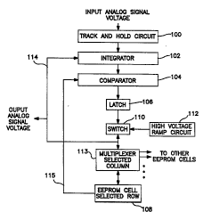
cell. ~L particular, Figure 2 illustrates a track and hold circuit 100, an
integrator 102, a ~ o~ 104, and a latch 106, each of which is a
portion of the analog column read/write circuitry 15 of Figure 1. Figure 2
also illu~trates a single EEPROM cell 108 connected through a lI.UI
113 and a switch 110 to a high voltage ramp source 112. An output of
latch 106 is connected to switch 110 for controlling the application of a
high voltage to EEPROM cell 108. MultipleAer 113 allows the high voltage
signal to be applied to one of the EEPROM cells of a single column of
oelL. ~ Figure 2, only one of the EEPROM ceDis of the column is
specifically illllctrAtPtl Application of the high voltage ramp signal to the
EEPROMs of the column is time mlllhrlP~P~1 to allow signals to be
cP-lllPnti~lly stored irl all cells of the column.
In use, an input voltage ~ to an analog signal level to
be stored is recei ved by track and hold circuit 100 from column decoder 26
(Figure 1). Track and hold circuit 100 samples tllie input analog signal and
holds the signal at a fixed Yoltage to which EEPROM cell 108 is to be set
to. The sampled voltage, held by track and hold circuit 100, is l, .. .,~", i
to integrator 102 which operates to determine a target voltage for
applying to EEPROM cell 108. The target voltage is initially set to a value
less than the sampled volhge value such as, for example, 90% of the
sampled voltage value.
The target voltage is l, O I I~ .,.i to ~ . " "1 /~ ". l~ ., 104 which
compares the target voltage with the current voltage held within the
EEPROM cell which initially may be zero. The current voltage of the
EEPROM ceDi is provided to ~ ,,. nll " 104 along a ~ P. I i. .., line 115.
As wiDi be described more fu~ily below, the voltage provided to the
~ ). along line 115 is .1. h . - - - i . ~PI1 during a "read-while-writing"
operation which is separate from a normal read operation. t~
104 outputs a signal which indicates whether the target voltage exceeds

W0 96/08823 Ç~ PCTIUS95/11590
~ -10-
the voltage of the EEPROM cell. The signal output from the .. ,...~ . ,. is
fed through latch 106 for controlling switch 110. So long as the target
voltage is greater than the voltage output from EEPROM cell 108 along
line 115, switch 110 remains closed to allow a high voltage ramp signal to
be applied to the EEPROM cell for uniformly mcrea3ing the voltage of the
cell. Once the voltage of the cell reaches the target voltage, the output
signal from - ,- - -l ,_ . rl 1- - 104 change3 state causimg latch 106 to open switch
110, thereby ] i~ the high voltage ramp from the EEPROM cell.
In this matter, the EEPROM cell is set to a voltage value cllhst~fi~lly
identical to the initial target volhge value.
Thereafter, a normal read operation is p~l~v~ ed on EEPROM cell
108 and the read voltage is conveyed, along a .. P. ~ - Ime 114, to
integrator 102 which operate3 to determine a new target voltage. More
particularly, integrator 102 operates to determine the difference between
the sampled voltage and the voltage provided along line 114 and to define
a new target volhg equal to, for example, the irlitial target voltage plus
90% of any L~ g difference between the stored voltage and the
sampled voltage. In other words, the new target voltage is set to about
99% of the sampled voltage. The actual level of the new target voltage
may differ bVlllt:WIlal from 99% depending upon the actual voltage stored
within EEPROM cell 108 which may vary as a result of L~ Lul~ and
otherfactors. Thenewtargetvoltageisthenappliedto...",l,_,,.l.-. 104
and the foregoing steps are repeated to again apply the high voltage ramp
to EEPROM 108 for in~rP~cing the voltage held therein to the new target
voltage. A~3 before, a read-while-writing voltage is output from EEPROM
celllO8and l,.."~".ill--~l alonglinell5to(...,.l,~ ..104. Oncethe
EEPROM cell reaches the new target voltage, latch 106 again operate3 to
open switch 110 thereby d~a~Liv.llilLg the high voltage ramp. A normal
read operation is again p~lr~,.l..~d to determine the actual voltage held
withinEEPROM cell 108 and ~he "normal" read voltage is l. ,...!....;11~.1
along line 114 to irltegrator 102.
Another new target voltage is calculated by mtegrator 102 with the
new target voltage beimg equal to the sum of the previous target voltages
plu~c, for example, 90% of any remair~ing difference between the sample

~76al0
WO 96/08823 ~ t ,;, PCT/US95111590
voltage and the actual voltage held within EEPROM 108. The new target
voltage is again applied to the EEPROM while a read-while-writing
voltage is him~ P-~uhly output from the EEPROM.
The overall sequence of storage cycles wherein hrget voltages are
r1Pt~rminf~d and applied to EEPROM cell 108 are p~ l~vlllled a
rl.-. . "i, .15,~ number of times and may be p. . rl,. " P~1~ for example~ four
to six times. The actual number of times for any particular system
l..,lr"l~l;l..,maybe.lPlr,...i,.~.1basedontheparticularneedsand
( 1)1 Ih~ of the system and is preferably chosen to yield the best trade-
off between speed and accuracy. Too few cycles may result in the cell
being under-~lv~"., . " "P.~ Too many cycles may result in a needless
amount of time spent and further results in a risk of over-~ . ., l . ", . i. .~Although it is advantageous to define a !!lr~Plrl ~ ~ ~i P. I number of cycles,
in other ill~ . l lrl l l~ c * may be desirable to allow the total number of
cycles to be dynamically, and perhaps av.l~iv~ly, controlled. For
example, ~ 1itir~n~1 circuitry may be provided which compares the actual
EEPROM cell voltage to the sample voltage and ~ . ., ,il ,~IPS the write
cycles once the difference ll~lebt~ ..l decreases below a minimum
pr~ ",j,lp.1 threshold.
Although Figure 2 illustrates only a single EEPROM cell, the
foregoimg VtJr lrllivlls are applied to all cells within the analog storage
device. The cells are arramged in columns and rows with each group of
columns havmg a column driver which contains a separate track and hold
circuit, integrator circuit, l l~ .., latch and lllulLi~ -Ar-l.
A small number of reference cells (not shown) may be provided for
storing a reference voltage for illl~JlVVillg the effective pr~ r~ r of the
track and hold circuits and for improving rejection of various
1 rC Overall read accuracy can be further improved by using the
referenoe cells to remove ~ r lrllul~ variation errors. In particular, the
stored ,~ f~ r~1 cell is forced to the reference voItage during the read.
The value of the voltage on a clear gate of the EEPROM cell (described m
more detail below with a reference to Figure 5A) is adjusted during the
read to thereby restore the reference voltage to the correct value. At the

wos6/oss23 ~,~6~ 12- pCT/US95/11590
same time, all voltages from the row ....~ the EEPROM cell are also
restored. These voltages can be read back r-~ntin~ cly with the
variation errors thereby removed. ru-~lrlll.ul~, better
ulr ~olll~rl~dlio~l can be achieved for cells recorded at different
Lrl I l~rlalulrs by using a reference cell for each EEPROM celL Such may
be required for systems which store samples with rn a single row which
are recorded at widely spaced time rntervals. The array can be recorded
one cell pair at a time, with each pair having one reference cell and one
signal cell. Slight over-program of the signal cell can be corrected by
slight A~litirm~l program of the paired reference cell. Por example, by
employing a pair of cells to sto}e each value, Irul~Jrlalulr variations or
other errors can be corrected during both storage and output of the analog
signals. One of each pair of cells is employed as a reference cell. The clear
gate voltage of the reference cell is adjusted to correct for the Irlll~rlalulr
variation or other errors. In this regard, the reference cell rl, . ,,. I~;r~ I Irl ~l
ctrAtl~ in Figure 5B may be employed. A particular ..., ,., I~,rl ~ Irl ll of
EEPROM cells in~ul~lalillg reference cells is illustrated in Figure 1 of
U.S. Patent No. 5,126,967 and the features illustrated therein, which relate
to the provision of reference storage columns, may be employed within
int~gr~t~-l circuit embodiments of the present invention as well. Many of
the details of the . ., ~Illgrllli~ll of columns of EEPROM cells and of the
reference column of cells are not pertinent to the present mvention and
therefore will not be described in detail herem.
It should be noted that each write high voltage ramp should be
carefully controlled so that each cycle of the write high voltage is
sllhst~nti~lly identical. In particular, the EEPROM cell should be exposed
to identical rl~nl1itit~nc each cycle of the write high voltage ramp except for
the value of the target voltage and the charge stored in the EEPROM cell.
As such, if the target voltage is held con~tant from one cycle to the next,
the output of the EEPROM cell while the high voltage ramp is applied will
reach the target voltage before any additional charge is placed onto the
EEPROM cell. Hence, no further wdting of the cell will occur because the
EEPROM cell will have reached the target voltage at its output before any
chamges can be made to the stored voltage. If the cell becomes slightly
over~ 1, then the target voltage is ~ r~al~ly reduced dudng
. , . . , . . . . _ _ _ _ .

WO96/08823 2~7So10 ,-c j PCTIIJS9~ 90
the next cycle. This ensures that no further change to the voltag of the
EEPROM will be made by Arl~1itionAl write cycles.
Thus the method for ~l..~. ,...., ..;, .~ the analog voltdge value
p~-l r~ by the system of Figure 2 operates to adjust the stored voltage
based on the mput voltage and on the actual voltdge stored in the cell.
The method therefore is an adaptive method. Hence, even when many
cells are bemg written at the same time, mdividual cell variations are
.".I~.".~Ii.,-lly~U~ l~dl~d~
Referring to Figures 3 - 5, details of the ~,:Ulll,UUll~ of Figure 2 will
now be set forth. Figure 3 illustrates track and hold circuit 100
illl~l..ll~lll~d as a switched capacitor track and hold circuit including a
capacitor 116 and an u~laliullal amplifier 118. Capacitor 116 is connected
through a switch 120 to an mput voltage Ime (Figure 2). Capacitor 116 is
also connected to the inverting input of v~u~aliulldl amplifier 118. A
second switch 122 is connected which bypasses .~.~. ,. I ;....~l amplifier 118
between capacitor 116 and an output Iine 125 connected to integrator 102
(Figure 2). Switch 120 can also connect capacitor 116 directly to output
line 125.
During a ~rack mterval, switch 120 is controlled to connect the
mput Iine to capacitor 116 while switch 122 is kept closed thereby storing
both the offset voltdge and the input onto the capacitor. During a hold
interval, switch 120 is controlled to connect capacitor 116 to output line
125 while switch 122 is left open. The offset volhge of the u~ la~iul-al
amplifier is ~u, I~ t~'y canceled by this , r,~; ,- I i- ~" However, the
charge feed through of switch 122 is not canceled and such may limit
accuracy of the stored value. AL~uldill~ly~ a minimum gdte area switch is
~ Ial~ly used. Storage capacitor 116 preferably has a high ~rA. it~n~-p,
such as 5 ri~ rA~c (pF). The high rArAritAn( P helps achieve both a long
hold time and high accuracy.
Another capacitor (not shown) may also be provided between
output 125 and switch 120 to prevent unwanted transients on output 125.
With a suitable choice of z.r~ritAnfP, the presence of the ~ liti~nAl
capacitor will not change the desired operation of the circuit.

WO 96/~8823 2 1~ S O 1 ~ - PCT/US9~ 90
-14-
Circuit ~-~h~m~til~ of an ~ aly ,~llyl~ n of integrator
102 are also set forth in the Appendix as c. l .~. . .~ I il !. A and B. With brief
reference to elements within ~. l .~,, ~ l i. ~ A and B, when a logic input
"DIFB" is held high, then capadtors C3 and C4 are cormected together and
a voltage difference between "V1" and "DRA~" is used to increment the
new target voltage on the output. Control signals S1 and S2 sample the
two input voltages "V1" and "DRAIN" and force charge into node "INM"
which is the amplifier mput. Sinoe the gain of the amplifier is very large,
the feedback capacitor C2 provides an opposite charge. This action
changes the output voltage by a voltage ~lvluul Llul~al to the capacitor ratio
of the sum of C3 and C4 divided by C2. The ratio should be less than one
and may be set to 0.9. This is the ~ inn used for a program such
as m Figure 2.
Referring again to Figure 2, column, ....I .~ ., I .)l 104 will now be
briefly described. ('.. I~ .. 104 is a high gain and high speed
...... 1 . ,.l... used to turn off the voltage ramp applied to the EEPROM cell
being pl.. ~ l .. o.~ Such occurs during the read while write interval ofthe overall write cycle. The read while write mterval may be a very
"noisy" mterval. Hence, ~ 104 preferably includes three
differentialgamstages(notspecificallyshowninFigure2)for..l,~lvv..,g
rejection of both ground amd power supply noise. An exemplary
,l,o,i..l,~: -l of ~ - 104 having the three ~iffl~rl~nti~l gain stages is
set forth rn the Appendix as s~hPm~tirc C, D and E.
High volhg power switch 110 will now be described with
reference to Figure 4 which provides an ~ L~ly ~ o.lill,~,l. As
noted above, the function of switch 110 is to apply a high voltage to the
cell being ~IV;1 A - ~ (through column multiplexer 113). ïn the circuit
of Figure 4, the high voltage is identified as the CHV column high voltage
produced by a charge pump (not shown) as a 0 volt to 20 volt 100
, .. i.. æ. ~. .1 ramp the pump repeats at a 125 ll~ v~c ulld rate. Switch
110 is a bou~ ,ed high side switch with three logic controls and a
smgle output COLN.

~ 2176D ,,jj .;~,
WO 96108823 l o ' PCTI~S95/11590
-15-
Briefly" I~n~ Prin~ some of the features o~ the circuit of Figure 4,
control signals employed are WR (a write signal) and HENB (a high
voltage enable bar signal). For a write operation, WR is high with HENB
low and CHV also low. This state charges a bootstrap C2 capacitor to
about four volts positive on node 8. The voltage on CHV is then increased
until a desired write voltage is prPsent on the source of the progr~mmPrl
cell. HENB is driven high by latch 106. This state rapidly di~ a~ s node
8tofivevolts. Thisvoltagepreventsfurther~lv~"....",;"~butisstillhigh
enough to prevent M4 from drawing current due to gated diode
breakdown.
For read operation, the gate voltage on M4 is driven to 0 volts. This
state prevents any current flow between CHV and COLN during the
read. To enter tllis state, WR is brought low, then DSCH is driven high.
No steady power supply current is drawn.
The HENB signal is applied through C3 to discharge node 8.
During DSCH high the signal HENB should be returned to low. This
chargPs C3 while node C3B is held at VSS by DSCH. During the read
operation, the DSCH signal should be high to assure that M4 is held of
Referring again to Figure 2, mllltirlPYPr 113 will now be further
described. Multiplexer 113 is connected to each column of the array for
allowing the volhge provided by high volhge ramp circuit 112 through
switch 110 to be ind~.d~l,Lly applied to each EEPROM cell 108 within a
column. Each column has a separate multiplexer.
In an ~ Jlaly PmhorlimPnt of multiplexer 113, each column has
32 cells requiring a 1:32 multiplexer. This may be implemented using an
initial 1:4 select followed by four 1:8 selects.
Referring to Figure 5A, EEPROM cell 108, will now be described.
EEPROM cell 108 includes a source transistor 124 and a drain transistor
126. The high vl~lhge ramp signal provided by ramp circuit 112 of Figure
2 is applied to a source of transistor 124 which also receives a 20 volt select
signal at its gate. Transistor 126 receives a 3.5 to 0.0 volt ramp clear signal
ât its gate. A "read while write" voltage line is connected to a drain of

wog6/oss23 2l~al~ PCT/US95~ll590 -
-16-
transistor 126 which is also connected to a current source.
During a write operation, the high volhge ramp signal is applied to
the source of transistor 124 while the read while write volhge is
cim~ P~ .ly detected from the drain of transistor 126. ~ this manner,
the voltage level held by EEPROM 108 is detected while the voltage level
is being set. This is in contrast to typical EEPROM cells, such as those
described within the patents referenced above, wherein a read operation
cannot be pr. r. ,., ..PIl cim~ 1.y with a write operation. Within such
EEPROM cells, there is no output -, P l ;- -, to the drain transistor.
Rather, the source transistor is either connected to a high voltage ramp or
to a read voltage line. As such, the analog signal level stored within the
EEPROM cell canrlot be both read and written to ciml~ltPl~P~llcly
As noted, in one embodiment each colurnn of the memory array
includes thirty-two EEPROM cells. In that ~."bo~,l.l~,l the read while
write voltage line should be isolated every thirty-two cells to reduce the
total ~ ll r on the line during the write. The select gate of the
EEPROM cell of Figure 5A is employed to isolate all other rows of the
storage array (which may total for example, 128). Preferably, the clear
gate of transistor 126 is shorted with an implant for a lead connected to
the read while write voltage lirle. Further isolation is achieved by
providing an active layer, which isolates each group of thirty-two
EEPROM cells to separate gro~ps, i.e., to node up-and-down groups. By
employing the select gate of the EEPROM cells to isolate every thirty-two
cells and to thereby reduce the total rPr~ri~nro on the line, increased
writing speed is achieved.
Referring to Figure 5B, an alternative embodiment of the EEPROM
which provides for a lr ..l~r. ,.l, ..~ corrected read is illllctrPtr-l The
.,bo,1...,~,~ of Figure 5B is sirnilar to that of Figure 5A and like elements
are identified with like reference numerals with primes. For the
ell~l)oll .~ l of Figure 5B, a normal read ~ line l25' is connected
to the source of transistor 124' and to a current source 127' for p~:.rul.l,.. ,g
a normal read operation. To provide a I rl 1 1~ corrected read, the
normal read ~ rl ;~ .. . line l25' of a reference cell is connected through a

~ 1 760 ~
WO 96/08823 '9 ~ - PCT111S9SIIIS9O
-17-
129' to the VCLEAR gate of the cell with the ~ . also
receiving a reference voltage. The VCLEAR gate of the reference cell is
common to an entire row of storage cells. By feeding the normal read
voltage and a reference voltage through a ~ '''''l'~'~'l''' onto the VCLEAR
gate, the voltage ~Df the VCLEAR gate can be forced to a voltage selected to
correct for l~ p~:lalull: and other factors for the entire row of cells. This
~ rL~iv~ly allows ~ ~ "~ read operation. It should be noted that the
normal read line illllctr~t~-l in Figure 5B is employed within the
embodiment of Figure 5A. However, for the ~".bodi".~:,.l of Figure 5A,
the normal read line is not routed through a ' "" 'l"" "I~ ~ into the VCLEAR
gate.
What has been described thus far is a voltage program method and
apparatus for use with a system wherein a single EEPROM cell is
employed for storing each input signal value. Referring to Figure 6, an
alternative .:, . .bo.li".~,.l of the invention wherein a pair of EEPROM cells
are employed to store each analog signal value as a difference voltage will
now be described. The alternative t:,,.bo-li,,.~,lL of Figure 6 is similar to
ther~ lil"rlll of Figures2-5Bandsirnilaroridentical~u".~".~.L~will
not be re-.ll~c- nl~
Figure 6 illustrates two read-while-writing circuits similar to the
single circuit of Figure 2 but each including a modified intf~r~t~lr. Within
Figure 6, elements similar or identical to those of Figure 2 are illllctr~t~
with like reference numerals i, .. . ~ 1 by 100. Elements of a first
circuit are denoted with subscript 1 and elements of a second circuit are
denoted with subscript æ For example, the first of the pair of circuits
includes a track and hold circuit 2001, a .~ . .. 2041, a latch 2061, etc.
The second of the pair of circuits includes a track and hold circuit 2002, a
' ""'l'~' ~l~ 2042, a latch 2o62~ etc.
The modified i~ . of the two circuits are ,~e.liv~ly
denoted 2501 and 2502. Whereas integrator 102 of Figure 2 receives only
two inputs, one from the track and hold circuit and the other from the
EEPROM cell, i. ~ I r~ ,. 1. ., . 250l and 2'iO2 each include two ~rl ~ihrm~l
inputs. In particular, imtegrator 2501 receives input along a line 2012 from

WO 96108823 ~ PCTIUS95111590
-18-
track and hold circuit 2002. Likewise, integrator 2502 receives rnput along
line 2011 from track and hold circuit 2001. Integrator 2501, also receives
input from EEPROM output ]ine 2142 of the second circuit. Likewise,
integrator 2502 receives rnput from line 2141 of the first circuit. Hence,
each of the i~ receives input signals from its own track and hold
circuit and EEPROM cell and also from the track and hold circuit and
EEPROM cell of the other circu*. The function of modified illl~ dll .~ .
2501 and 2502 is to improve the accuracy of the voltage difference stored
into EEPROM cells. This difference voltage is driven to be equal to the
voltage difference between separate input signals Voltage A and Voltage
B.
A first set of write cycles are conducted as rn the embodiment of
Pigure2. Afterapreselectednumberofcyclesofwriting,i~ ldllll~25
and 2502 measure both the dif.ference between its track and hold output
and EEPROM "normal read" voltage and the track and hold output and
"normal" read voltage of the paired cell. The difference values are
buLLIac~d one from the other value. This "difference of two dirLl~l..t ,"
is used to adjust the target vol~ages at the output of the i ~ ~ I r~l .~ I ' 1' ~ to
correct for any small under- or over- program of the pair of EEPROM
cells. The ability to correct for small over program is a key to improved
accuracy. If one of the input voltages is a reference voltage, then the
output of that cell can be used to restore the exact voltage of the other
input. If both inputs are employed as differential signals, then the voltage
swing range of the output differential signal is twice as large as can be
stored into a single EEPROM cell.
The . . .~ . d 1 l ll described "difference of two .1 i rr~ ." may be
illll~l. .ll~lllr~1 usingthecircuitofSchematicBwhenlogicinput"DlFB"is
held low. As such, capacitor C4 is no longer cormected together with C3,
but is switched by two control signals Sl and S2 between "DRA~2" and
"V2". Because the two inputs to capacitor C3 are reversed, the difference
voltage between the two inputs is subtracted from the output by the ratio
of 0.45, C3 divided by Q. Fo]r the inputs "Vl" and "DRAIN", the ratio of
C4 divided by C2 is the same 0.45 value.

~ %1 7sol~ , .
WO 96/08823 - - -- PCT/US95/ll~i90
-19- ~ ~
Both EEPROM cells 208l and 2082 receive the same number of
write cycles. The number of cycles can be selected by digital EEPROM
program bits. Default values may be set to four cycles of regular write
and one cycle of ~ifff~r~nti~1 write. The ~iffior~nh~l write will always drive
one target voltage up and the other down by the same amount. The
intended operation is as a final very small ~ llrlll of the read volhge
difference between the two EEPROM cells.
Now some examples of the ~iff~r~nti~1 write ~ clLiu-~ p~:lrull~ed
by the system of Figure 6 are provided.
If the two EEPROM cells are already set to be exactly correct when
the ~]irr~ l wr*e is ~ nmm~n~ then the two target voltages at the
outputs of the; ~ r are not changed and the write operation is
repeated. Since mo change is made in the target voltages, little or no
change is made in the charge stored in the EEPROM cells by the final
write cycle and the final read voltage difference will be the desired value.
If one cell is exactly correct, but the other EEPROM cell has a read
voltage slightly higher than desired, the target voltage of the correct
EEPROM cell is increased slightly and the target voltage of the other cell is
decreased by the same amount for the ~liff~r~nti~1 write cycle. This
.Ll--~--lbringsthereaddifferencevoltagebetweenthetwoEEPROM
cells closer to the desired value.
Lf one cell is correct and the other is still slightly low, then the target
for the correct celI is decreased while the hrgt for the low cell is
increased for the write cycle.
If both cells are high or low by the same volhge, then the hrget
voltages are not changed since the read difference voltage is correct.
Hence, once the ~ iti~n~1 write cycles are p~lr.~ ed, the
difference voltage between the two EEPROM cells 208l, and 2082 very
precisely matches the rnput analog signal volhge. Thereafter, any read
u~ . ,. I i.. s are ~ ~. r.. ~.1 from both EEPROM cell 208l, and EEPROM cell
2082 and the difference volhge is ~ (1 therefrom. In an alternative

w0 96/08823 ~ 6~ 20- ` pCllUS95111~90
dil~ lL, not shown, the input analog signal voltage may be stored as
an average of the voltages of the two cells. The supplemental
lulu~-.-~-----i,-~cycles,describedl;~ ..P~ t~l)/above,maybeemployedm
such an embodiment to adjust ~e voltage of one of the cells by a selected
amount such as the average be~ween the two voltages precisely matches
the mput analog signal voltage.
With reference to Figure 7, a particular application of the analog
storage system will now be described. Within the system of Figure 7, an
analog storage circuit 300, ., ., . r;~,. . . ~.1 in accordance with either of the
embodiments described above, is in~ul~uldLed as a ~u~ uul~ -L in a high
density digital storage system. An input digital to analog converter 301
produces an analog voltage to represent a digital input. A controller 302
rnstructs analog storage circuit 300 to record the analog voltage at a
known location in the memory array. When the digital data is desired,
controller 302 fetches the analog output voltage from analog storage
circuit 300 and rnstructs analog to digital converter 303 to convert the
analog values and output digital data. The use of many level analog
signals to represent digital data gives a large increase in storage capacity
over digital systems. In the embodiment of Figure 7, each mdividual
analog storage cell actually stores digital data as discrete predefined
voltage levels. With sixteen discrete levels per cell, each cell thus stores a
four bit digital value. Six bit digital values may be stored within each cell
by employing sixty-four discrete levels per cell. As can be d~ idL~d, by
achieving a high density of analog storage, numerous applications which
were not h.orPtnfnre feasible now become feasible.
What has been described is a method and apparatus for
IUlu~ the voltage level of a storage cell, such as an EEPROM cell,
within an analog storage system. The mvention is advan~ol-cly
employed within systems for storing a wide range of analog signal
; ~ ~ r.. ., .. ~ I i nl . includmg voice and music signals. In one embodiment, the
imvention is employed within a digital data storage system wherein the
digital data is converted to analog form, then stored within analog storage
cells having a higher storage density than ~ul~v~l-Liullal digital cells.

WO 96/08823 lo -21- = PCT/US95/11~90
Although particular embodiments and applications of the
invention are described herein, such are intended to be merely illustrative
of general principles of the invention and should not be construed as
Iimiting the scope of the invention. Rather, general principles of the
invention may be exploited in a wide variety of applications and in a wide
range of embodiments.

Representative Drawing
A single figure which represents the drawing illustrating the invention.
Administrative Status

For a clearer understanding of the status of the application/patent presented on this page, the site Disclaimer , as well as the definitions for Patent , Administrative Status , Maintenance Fee  and Payment History  should be consulted.

Administrative Status

Title Date
Forecasted Issue Date Unavailable
(86) PCT Filing Date 1995-09-13
(87) PCT Publication Date 1996-03-21
(85) National Entry 1996-05-07
Dead Application 2003-09-15

Abandonment History

Abandonment Date Reason Reinstatement Date
2002-09-13 FAILURE TO PAY APPLICATION MAINTENANCE FEE
2002-09-13 FAILURE TO REQUEST EXAMINATION

Payment History

Fee Type Anniversary Year Due Date Amount Paid Paid Date
Application Fee $0.00 1996-05-07
Registration of a document - section 124 $0.00 1996-10-31
Maintenance Fee - Application - New Act 2 1997-09-15 $100.00 1997-08-25
Maintenance Fee - Application - New Act 3 1998-09-14 $100.00 1998-09-08
Maintenance Fee - Application - New Act 4 1999-09-13 $100.00 1999-07-15
Maintenance Fee - Application - New Act 5 2000-09-13 $150.00 2000-07-11
Maintenance Fee - Application - New Act 6 2001-09-13 $150.00 2001-07-16
Owners on Record

Note: Records showing the ownership history in alphabetical order.

Current Owners on Record
INFORMATION STORAGE DEVICES, INC.
Past Owners on Record
BLYTH, TREVOR
ENGH, LAWRENCE D.
Past Owners that do not appear in the "Owners on Record" listing will appear in other documentation within the application.
Documents

To view selected files, please enter reCAPTCHA code :


To view images, click a link in the Document Description column. To download the documents, select one or more checkboxes in the first column and then click the "Download Selected in PDF format (Zip Archive)" or the "Download Selected as Single PDF" button.

List of published and non-published patent-specific documents on the CPD .

If you have any difficulty accessing content, you can call the Client Service Centre at 1-866-997-1936 or send them an e-mail at CIPO Client Service Centre.


Document
Description 
Date
(yyyy-mm-dd) 
Number of pages   Size of Image (KB) 
Office Letter 1996-06-06 1 13
International Preliminary Examination Report 1996-05-07 2 57
Representative Drawing 1997-06-17 1 6
Cover Page 1996-08-15 1 13
Abstract 1996-03-21 1 42
Description 1996-03-21 21 767
Claims 1996-03-21 29 742
Drawings 1996-03-21 11 151
Fees 1999-07-15 1 43
Fees 2000-07-11 1 42
Fees 2001-07-16 1 36
Fees 1998-09-08 1 50
Fees 1997-08-25 1 43