Note: Descriptions are shown in the official language in which they were submitted.
2i 76052
TRANSDUCER HAVING A RESONATING SILICON BEAM
AND METHOD FOR FORMING SAME
BAQICGROUND OF THE INVENTIQN
Field of the Invention
The invention relates to apparatus such as
pressure sensors which include a force transducer
having a resonating silicon beam formed in a silicon
wafer, and particularly to a method for forming the
same.
Discussion of Prior Art
U.S. Pat. No. 5,090,254 to Guckel discloses a
polysilicon resonating beam transducer. The transducer
includes a beam of polysilicon which is mounted at its
ends in a silicon substrate or wafer. The substrate
and a polysilicon shell cooperate to define a cavity
around the beam. The cavity is sealed from the
atmosphere and evacuated to maximize the Q of the
resonating beam. Resonant excitation of the beam can
be accomplished in various ways, such as by capacitive
excitation. Vibratory motion of the beam may be
detected using an implanted resistor which is
piezoresistive. Formation of the beam is carried out
by depositing the beam on a sacrificial layer and
surrounding the beam in a second sacrificial layer
before the encapsulating polysilicon shell is formed.
The sacrificial layers are etched out with liquid
etchant which passes through channels in the periphery
of the shell. Following etching, the interior of the
2176052
-2-
cavity surrounding the beam is maintained in a wash
liquid so that the beam is not deflected toward any of
the adjacent surfaces, and the wash liquid is removed
by freezing and sublimation. The interior surfaces of _
the cavity and the outer surfaces of the beam are
passivated, and the channels leading into the cavity
are sealed by oxidation in an oxidizing atmosphere,
which also results in consumption of oxygen in the
cavity.
U.S. Pat. No. 5,242,863 to Xiang-Zheng et al.
relates to a silicon diaphragm piezoresistive pressure
sensor having a diaphragm formed by a single-sided
fabrication method. The diaphragm is formed with a
cavity thereunder by: a) forming a buried low
resistance layer under a predetermined diaphragm
region; b) epitaxially depositing a layer of silicon;
c) forming low resistance trenches through the
epitaxial layer which trenches are connected with the
buried low resistance layer at the edge of the buried
low resistance layer; d) converting the low resistance
trenches and buried low resistance layer to porous
silicon by anodization in a concentrated HF solution;
e) removing the porous silicon by etching; and f)
filling the openings formed by etching with polysilicon
to seal the cavity.
CA 02176052 2001-02-06
-3-
SCARY OF THE INVENTION
The invention provides apparatus including a
force transducer having a resonating beam that is
formed in a silicon wafer and which apparatus is of
relatively simple and inexpensive construction. As
used herein, the term beam should be interpreted
broadly to include microstructures such as tuning
forks, H-beams, cross beams, interleaved combs, and
spiral springs, etc.
The invention also provides a method having
relatively few manufacturing steps for forming
apparatus including a force transducer having a
resonating beam formed in a silicon wafer. In one
form, the method includes the steps of implanting in a
substrate a layer of either n-type or the p-type
dopant; depositing a doped epitaxial layer on the upper
surface of the substrate (wherein the dopant in the
epitaxial layer i.s the opposite from that type of
dopant in the substrate, i.e., if the substrate has
therein a p-type dopant, then the epitaxial layer
includes an n-type dopant and vice versa); implanting a
pair of spaced sinkers through the epitaxial layer and
into electrical connection with the epitaxial layer,
each of the sinkers including either the n-type or p-
type dopant; anodizing the substrate to form porous
silicon from the sinkers and the underlying doped
substrate layer; oxidizing the porous silicon to form
CA 02176052 2001-02-06
- 4 -
silicon dioxide; and etching the silicon dioxide to form
the cavity and beam..
It is an advantage of the invention to provide
a method of forming a single crystal resonating beam
within a cavity, which beam facilitates the placement: of
electronic circuitry directly on the beam.
According too one aspect of the invention, there
is provided a methcd of forming apparatus including a
force transducer hav_Lng a resonating silicon beam within
a cavity in a silicon substrate, the method comprising
the acts of:
a. providina-t~he silicon substrate having an upper
surface;
b. implanting a buried layer of a dopant, the
dopant being one of the n-type and the p-type dopant,. in
the substrate;
c. implanting in the substrate a layer of a dopant
of the other of the n-type and the p-type over the buried
layer of the one of the n-type and the p-type dopant,;
d. depositing ar. epitaxial layer on the upper
surface of: the sub~~t:rate to completely cover the layer of
dopant, the epitaxi.a:1 layer including a dopant of the one
of the n-type and the p-type;
e. implanting a pair of spaced sinkers through the
epitaxial layer and into electrical connection with l~he
layer of c~opant, eacz of the sinkers including a dopant
of the other of the :~-type and the p-type;
f. anodizinc3 the substrate to form porous silicon
of the sinkers and t:he layer of dopant;
g. oxidizing the porous silicon to form silicon
dioxide;
CA 02176052 2001-02-06
- 4a -
h. dissolving the silicon dioxide by etching to
form the cavity and t:he beam supported within the cavity
to resonate within the cavity, so that the cavity
includes a pair of spaced side walls, a pair of spaced
end walls extending between the side walls, and a bottom
wall, and so that the beam extends from one of the end
walls of the cavity to the other of the end walls of the
cavity, and so that t:he beam has side surfaces spaced
from the side walls of the cavity and a lower surface
spaced from the bottom wall; and
i. providing a capacitive drive for causing
resonant motion of the beam, the capacitive drive
including a first electrode below the beam, a second
electrode in the bears, and a third electrode above the
beam wherein the buried layer of the one of the n-type
and the p-type dopant~ acts as the first electrode.
According t;o another aspect of the invention,
there is provided a rnethod of forming apparatus including
a force transducer having a resonating silicon beam
within a cavity in a silicon substrate, the method
comprising the acts of:
a. providing the silicon substrate having an
upper surf ace ;
b. implanting a buried layer of a dopant, the
dopant being one of the n-type and the p-type dopant, in
the substrate;
c. implanting in the substrate a layer of. a
dopant of the other' of the n-type and the p-type over the
buried layer of the one of the n-type and the p-type
dopant;
d. depositing an epitaxial layer on the upper
surface of the subw~t:rate to completely cover the
CA 02176052 2001-02-06
- 4b --
layer of dopant, the epitaxial layer including a dopant
of the one of the n-type and the p-type.
e. implanting a pair of spaced sinkers
through the epitaxial. layer and into electrical
connection with the layer of dopant, each of the sinkers
including a dopant of t:he other of the n-type and the p-
type.
f. anodi~:ing the substrate to form porous
silicon of the sinkers and the layer of dopant;
g. oxid:i~:in~~ the porous silicon to form
silicon dioxide;
h. form:inc~ a sacrificial layer over the
epitaxial layer;
i. form:ing over the sacrificial layer a cover
layer;
j. dissol.vi:ng the silicon dioxide and the
sacrificial layer by etching to form the cavity and the
beam supported within the cavity to resonate within the
cavity, so that the cavity includes a pair of spaced side
walls, a pair of spaced end walls extending between the
side walls, a bottom wall, and a top wall, and so that
the beam extends from o:ne of the end walls of the cavity
to the other of the end walls of the cavity, and so that
the beam has side surf=aces spaced from the side wall's of
the cavity, a lower ~~urface spaced from the bottom wall
and an upper surface spaced from the top wall;
k. prov:ic~ing a capacitive drive for causing
resonant motion of the :beam, the capacitive drive
including a first electrode and wherein the buried layer
of the one of the n-type and the p-type dopant acts as
the first electrode of the capacitive drive.
According t:o a further aspect of the invention,
CA 02176052 2001-02-06
- 4c _
there is provided a rnethod of forming apparatus including
a force transducer having a single crystal resonating
silicon beam within. a cavity in a single crystal silicon
substrate, the method comprising the acts of:
a. providing the single crystal silicon
substrate having an. upper surface;
b. implanting a buried layer of a dopant, the
dopant being one of the n-type and the p-type dopant, in
the substrate;
c. implanting in the single crystal substrate
a layer of a dopant of the other of the n-type and the p-
type over the buried layer;
d. depositing an epitaxial layer on the upper
surface of the single crystal substrate to completely
cover the layer of dopant, the epitaxial layer including
a dopant of the one of the n-type and the p-type;
e. implanting a pair of spaced sinkers
through the epitaxial layer and into electrical
connection. with the .Layer of dopant, each of the sinkers
including a dopant of the other of the n-type and the p-
type;
f. anodi~:ing the substrate to form porou:~
silicon of the sinkers and the layer of dopant;
g. oxidising the porous silicon to form
silicon dioxide;
h. dissolving the silicon dioxide by etching
to form tr.e cavity and the single crystal silicon beam
supported within the cavity to resonate within the
cavity, sc~ that the cavity includes a pair of spaced side
walls, a pair of spaced. end walls extending between
the side walls, and a bottom wall, and so that the beam
extends from one of i~ize end walls of the cavity to the
CA 02176052 2001-02-06
- 4d -
other of the end walls of the cavity, and so that the
beam has side surfaces spaced from the side walls of the
cavity and. a lower surface spaced from the bottom wall;
and
i. providing a capacitive drive for causing
resonant motion of the beam, the capacitive drive
including a first elc=_ctrode below the single crystal
silicon beam, a second electrode in the beam, and a third
electrode above the beam and wherein the buried layer
acts as tile first ele~trode.
Other features and advantages of the invent=ion
will become apparent to those skilled in the art upon
review of the following detailed description, claims, and
drawings.
BRIEF DESCRIPTION OF THE DRAWINGS
Fig. 1 i~~ a cross-sectional view of a force
transducer die embodying various of the features of the
invention and taken along line 1-1 of Fig. 26.
Fig. 1A i.s a cross-sectional view of a forage
transducer die taken along line lA-lA in Fig. 1.
Fig. 2 i:~ a cross-sectional view similar to
Fig. 1 and showing a buried n-type layer implanted i:n the
substrate.
Fig. 3 i;~ a buried n--type layer mask used in
the process of creating the buried n-type layer shown in
Fig. 2.
Fig. 4 i;~ a view similar to Fig. 2 and showing
a buried p-type layer.
Fig. 5 i:~ a buried p-type layer mask for
patterning the buried p-type layer shown in Fig. 4.
217652
-5-
Fig. 6 is a view similar to Fig. 4 and
showing an n-type epitaxial layer and two p-type
sinkers.
Fig 7. is a p-type sinker mask for patterning
the p-type sinkers shown in Fig. 6.
Fig. 8 is a view similar to Fig. 6 and
showing an n-type sinker.
Fig. 9 is an-n-type sinker mask for
patterning the n-type sinker shown in Fig. 8.
Fig. 10 is a view similar to Fig. 8 and
showing a precavity region.
Fig. 11 is a view similar to Fig. 10 and
showing p-type layers defining a capacitor middle layer
and piezoresistor.
Fig. 12 is a capacitor and piezoresistor mask
for patterning the p-type layers defining the capacitor
middle layer and piezoresistor shown in Fig. 1I.
Fig. 13 is a view similar to Fig. 11 and
showing a sacrificial layer.
Fig. 14 is a sacrificial layer mask for
patterning the sacrificial layer shown in Fig. 13. -
Fig. 15 is a view similar to Fig. 13 and
showing a cover layer and anchors.
Fig. 16 is an anchor mask for patterning the
anchor cavities shown in Fig. 15.
Fig. 17 is a cover mask for patterning the
cover layer shown in Fig. 15.
-6-
Fig. 18 is a view similar to Fig. 15 and
showing an upper p-type layer implanted in the cover
layer.
Fig. 19 is an upper p-type layer mask for
patterning the upper p-type layer shown in Fig. 18.
Fig. 2O is a view similar to Fig. 19 and
showing a cavity and open etch channels.
Fig. 21 is a view similar to Fig. 20 and
showing the sealed etch channels and an insulating
layer.
Fig. 22 is a view similar to Fig. 21 and
showing electrical contact cavities.
Fig. 23 is an electrical contact mask for
patterning the electrical contact cavities shown in
Fig. 22.
Fig. 24 is a view similar to Fig. 22 and
showing metal electrical contacts.
Fig. 25 is a metal mask for patterning the
metal electrical contacts shown in Fig. 24.
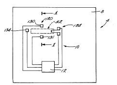
Fig. 26 is an illustration showing a force
transducer of the invention.
Before one embodiment of the invention is
explained in detail, it is to be understood that the
invention is not limited in its application to the
details of the construction and the arrangements of
components set forth in the following description or
illustrated in the drawings. The invention is capable
of other embodiments and of being practiced or being
~~ ~~fl~2
carried out in various ways. Also, it is to be
understood that the phraseology and terminology used
herein is for the purpose of description and should not -
be regarded as limiting.
DETAILED DESCRIPTION OF A PREFERRED EMBODIMENT
Illustrated in the drawings is an apparatus 4
formed on a silicon wafer or substrate 8 and embodying
various of the features of the invention. Although
different apparatus such as pressure sensors, strain
sensors and displacement sensors may be formed
according to the invention, in the illustrated
embodiment the apparatus 4 is a force transducer 10.
The force transducer 10 (Fig. 26) includes a resonating
beam formed as further described below.
The force transducer 10 also includes
integrated circuitry 12 formed on the substrate 8 and
connected to the force transducer 10. The integrated
circuitry 12 provides power for the force transducer 10
and converts output from the force transducer 10 to a
desired format. It will be appreciated by those
skilled in the art that the integrated circuitry 12 can
be suitably arranged in various configurations. The
configurations of the integrated circuitry 12 are known
and will not be described in further detail.
As shown specifically in Figs. 1 and 2, the
wafer or substrate 8 is a single crystal of silicon
which is altered as described below. The wafer 8
~176~52
_g_
includes spaced upper and lower side portions 16
(Fig. 2, lower side portion not shown). The upper side
portion 16 includes a horizontal upper surface 17.
Although the wafer 8 can be of any suitable thickness,
in the illustrated embodiment the wafer 8 is about 500
microns thick. An epitaxial layer is deposited on the
upper surface 17, as further described below.
A cavity 22 is defined in the upper side
portion 16. For purposes of describing the cavity 22,
the upper side portion 16 of the wafer 8 is taken to
include the epitaxial layer (i.e., as shown in the
drawings, portions of the cavity 22 are defined by the
epitaxial layer deposited on the upper surface 17).
The cavity 22 includes a pair of spaced side walls 28,
a pair of spaced end walls 32 extending between the
side walls 28, and a horizontal bottom wall 36
extending between the side walls 28 and end walls 32.
The side walls 28, end walls 32 and bottom wall 36 thus
cooperate to define the cavity 22.
The transducer 10 includes a beam 52 which is
supported in the cavity 22. The beam 52 has a
longitudinal axis and includes opposite end portions 56
(shown only in Fig. 1A) spaced along the longitudinal
axis. The end portions 56 are connected to and
integral with the end walls 32. The beam 52 being thus
supported can be described as an end-supported or
doubly-supported beam. Attachment of the beam 52 at
the end portions 56 allows strains in the wafer 8 in
2176~~2
_g_
the direction of the longitudinal axis of the beam 52
to cause changes in the resonant frequency of the beam
56. in the specific embodiment illustrated, the beam
52 is formed in the epitaxial layer 208 (Figs. 8 and
10). In other specific embodiments (not shown), the
beam 52 can be formed partially in the epitaxial layer
208 and in the upper side portion 16 of the wafer 8.
The beam 52 has a length defined between the end walls
32. Although the beam 52 can be of any suitable
length, in the illustrated embodiment the length of the
beam 52 is about 100 um. The beam 52 includes a lower
side 64 spaced from the bottom wall 36. The beam 52
also includes an upper side 68 spaced from the lower
side 64. The beam 52 has a thickness between the lower
and upper sides 64 and 68. Although the beam can be of
any suitable thickness, in the illustrated embodiment
the beam 52 has a thickness of about 1.5 microns. The
beam 52 also includes a pair of spaced sides 72
extending between the lower and upper sides 64 and 68
parallel to the side walls 28. The beam 52 has a width
defined between the sides 72, which in the illustrated
embodiment is about 20 microns.
The transducer 10 includes a cover layer 92
(Fig. 15) spaced from the upper side 68 of the beam 52.
The cover layer 92 is supported about its periphery by
the epitaxial layer 208 around the cavity 22. The
cover layer 92 cooperates with the side walls 28, end
walls 32 and bottom wall 36 to enclose the cavity 22
~
2i ~6ii52
-10-
and thus define a closed space about the beam 52.
Although any suitable material is appropriate, in the
illustrated embodiment, the cover layer 92 consists of
polysilicon having a thickness of about 2 microns.
Although the space between the cover layer 92 and the
upper side portion 68 of the beam 52 can be of any
suitable dimension, in the illustrated embodiment the
cover layer 92 is spaced about 1 micron above the upper -
side 68 of the beam 52. Preferably, the cavity 22 is
evacuated to minimize damping of the vibrations of the
beam, as further described below.
The transducer 10 includes means 120 (Fig.
26) for causing resonant motion of the beam. Although
any suitable means can be employed for causing resonant
motion of the beam, in the illustrated embodiment the
means 120 for causing resonant motion of the beam 52
comprises electrodes which cooperate to define a
capacitive drive 120. The capacitive drive 120
includes spaced lower, middle and upper electrodes or
conductive regions 200, 224a, and 229 (shown in Fig.
20). The lower conductive region 200 is an n-type
dopant, such as phosphorous, implanted in the substrate
8 below the bottom wall 36. The middle conductive
region 224a is a p-type dopant, such as boron,
implanted in the beam 52. The upper conductive region
229 is a p-type dopant, such as boron, implanted in a
polysilicon cover, as described below. The lower,
middle and upper conductive regions 200, 224a and 229
~
216052
-11-
are electrically connected to the integrated circuitry
12 to define a capacitor or capacitive drive. It will
be apparent to those skilled in the art that the beam
52 is caused to vibrate or resonate by operation of the
capacitive drive in a known manner. It is also
apparent that various combinations of dopants can be
used to form the electrodes 200, 224a and 229.
The transducer IO includes means 124 (Fig.
26) for measuring resonating motion of the beam 52.
Although any suitable means can be used for measuring
resonating motion of the beam, in the illustrated
embodiment the means 124 for measuring resonating
motion of the beam is a piezoresistor. The
piezoresistor 124 is created by implanting in the beam
52, a dopant, such as boron. The piezoresistor 124 is
connected to the integrated circuitry 12 in manner well
known to those of ordinary skill in the art. The
resistance of the piezoresistor 124 changes with strain
in the beam 52 in accordance with the piezoresfstive
effect, and thus permits resonance of the beam to be
measured in a known manner. It will be appreciated by
those skilled in the art that in different embodiments
(not shown) other specific arrangements of passive
electronic circuit elements such as a capacitor or
arrangement of active electronic circuitry can be used
for measuring the resonant frequency of the beam.
Moreover, the single crystal nature of the beam 52
allows the placement of active or passive signal
2i 7652
-12-
conditioning circuitry (not shown) to be implanted
directly on the beam 52.
The transducer 10 includes electrical
contacts 130, 131 and 134 for connecting the capacitive
drive 120 and piezoresistor 124 to the integrated
circuitry 12. In the illustrated embodiment, the
electrical contacts 130, 131 and 134 comprise
conductive material, such as aluminum, which is
deposited on the epitaxial layer 208. In other
embodiments (not shown), the electrical contacts may be
formed by dopants implanted to define conductive
regions .
The transducer 10 is formed on any suitable
silicon wafer or substrate 8. A suitable substrate 8
is a p-type silicon wafer of lightly doped P{100)
silicon having p-type boron dopant with a carrier
concentration between 1015 and lOlfi cm3, a <100> cut
lattice, 6.0-18.0 ohm-cm resistance. Wafers meeting
SEMI standard prime CZ or float zone, for example, are
suitable. Examples of other suitable silicon wafers
are those having lower concentrations of p-type or n-
type dopants than layers to be subsequently added to
the wafer, such that the dopant acts as an etch stop at
the boundary with the added layers.
The beam 52 having the specific construction
described herein is formed by altering the p-type wafer
8 according to the following steps:
217b052
-13-
1. implanting buried n-type layer 200 in the
p-type wafer 8;
2. implanting buried p-type layer 204 over
the buried n-type layer 200;
3. depositing an epitaxial n-type layer 208
on the upper surface 17 of the wafer 8;
4. implanting p-type sinkers 212 and 216
through the epitaxial n-type layer 208 and into
connection with the p-type layer 204;
5. implanting an n-type sinker 220 through
the epitaxial n-type layer 208 and into electrical
connection with the n-type layer 200;
6. forming porous silicon of the p-type
layer 204 and the p-type sinkers 212 and 216 by
anodization;
7. oxidizing the porous silicon to form
silicon dioxide in a pre-cavity region;
8. implanting p-type layers 224, 225 and 226
in the epitaxial n-type layer 208;
9. depositing a sacrificial layer 228;
10. etching the sacrificial layer 228;
11. growing anchor oxide 227;
12. forming anchor cavities 231 by etching
anchor oxide 227;
13. depositing the cover layer 92;
14. implanting p-type layer 229 in the cover
layer 92;
15. etching the cover layer 92;
2176052
-14-
16. dissolving the sacrificial layer 228 and
the porous silicon dioxide by etching to form the
cavity 22;
17. sealing and evacuating the cavity 22;
18. depositing an insulating layer 234;
19. etching contact cavities 235 through the
insulating layer 234; and
20. depositing electrical contacts 232 for
connection to the integrated circuitry 12.
It will be appreciated by those skilled in
the art that various of the above-mentioned steps may
be omitted or altered in different specific embodiments
of the invention. For example, the steps regarding the
n-type layer 200, the n-type sinker 220 and the p-type
layers 224 and 226 may differ if different means are
employed for causing resonance of the beam or for
measuring the resonant frequency of the beam.
In the illustrated embodiment, the wafer 8 is
prepared for implantation of the buried n-type layer
ZO 200 by initially forming a screening layer of Si02 on
the upper surface 17 of the wafer 8. In the
illustrated embodiment, the screening layer of SiOz has
a thickness of about 5000 +/- 500 angstroms. The Si02
can be formed by any suitable means. In the
illustrated embodiment, oxidation to form the SiOz
screening layer is carried out by first "pushing" with
about 2.25 liters per minute (1/m) of NZ at a
temperature of about 550°C for a period of about 4
217b052
-15-
hours, ramping about 2.25 1/m of OZ gas at a rate of _._. _
about 20°C/minute, oxidizing with about 2.25 1/m of HZ
and OZ at about 1000°C, and then ramping with about 8
1/m of NZ at a rate of about 20°C/minute. The term
"pushing" as used herein means inserting the wafer into
the furnace. As also used herein, the term "ramping"
means changing the temperature in the furnace. The
SiOz screening layer is thereafter etched to achieve a
substantially uniform thickness. Etching with a 10:1
buffered oxide etching solution for a period of about 5
minutes is suitable. A suitable etching solution
includes about 40~ ammonia fluoride, 15?c hydrogen
fluoride and 45$ water. Those skilled in the art will
recognize that forming and etching a screening layer of
SiOz before each implant or deposition step may assist
in control of the subsequent implantation or deposition
step. In other embodiments, any of the screening
layers of Si02 may be omitted.
The buried n-type layer 200 can be implanted
by any suitable means. In the illustrated embodiment,
the buried n-type layer 200 (Fig. 2) is patterned by
applying photoresist and then exposing the photoresist
with the buried n-type layer mask shown in Fig. 3,
removing the mask, and then dosing with a suitable n-
type dopant. In the illustrated embodiment, the n-type
dopant is phosphorous, which is dosed at a
concentration of 5 x 10" cm 2 at 150 KeV. After the
photoresist is removed, the buried n-type layer 200 is
2i7b052
-16-
driven to a final thickness of about 3 microns by
thermal annealing. Thermal annealing can be carried
out in any suitable manner, such as by pushing with
2.25 1/m of NZ at 850°C for a period of about 30
minutes, ramping 2.25 1/m of 02 at a rate of
20°C/minute, oxidizing with 2.25 1/m of NZ at about
1050°C for a period of about 2 hours, and ramping with
8 1/m of NZ at a rate of 20°C/minute. The thermal
annealing conditions specifically described above are
provided for illustration, and those skilled in the art
will appreciate that different conditions may be used
to achieve this result.
The buried p-type layer 204 (Fig. 4) is
implanted over the buried n-type layer 200 by any
suitable means. In the illustrated embodiment, the
wafer 8 is prepared for receiving the p-type layer 204
by first etching for 5 minutes to remove the Si02
formed in the previous thermal annealing step. The
buried p-type layer 204 is patterned by applying
photoresist and exposing the photoresist with the mask
shown in Fig. 5. In the illustrated embodiment, the p-
type dopant is boron. The boron is dosed at a
concentration of 5 x 1013 cm z at energy levels of 50,
100 and 150 lZeV. After the buried p-type layer 204 is
implanted and the photoresist is removed, the buried p-
type layer 204 is driven by thermal annealing to a
final thickness of about 1 Vim. Thermal annealing can
be carried out by pushing with 2.25 1/m of OZ at 850°C
2~76u52
-17-
for a period of about 30 minutes, ramping 2.25 1/m of
OZ at a rate of 20°C/minute, annealing with 2.25 1/m of
N2 at about 1000°C for a period of about 10.5 hours,
and ramping with 8 1/m of NZ at a rate of 20°C/minute.
The n-type epitaxial layer 208 (Fig. 6) is
deposited on the entire upper surface 17 of the wafer 8
by epitaxial deposition. In the illustrated
embodiment, the wafer 8 is prepared for receiving the
n-type epitaxial layer 208 by etching to remove the
Si02 formed in the previous thermal annealing step.
The n-type epitaxial layer 208 is deposited in a
conventional manner. In the illustrated embodiment,
the n-type epitaxial layer 208 has a thickness of about
2 +/- 0.2 microns and a resistivity of about 0.35 +/-
0.05 ohms-cm.
The p-type sinkers 212 and 216 (Fig. 6) are
implanted in the n-type epitaxial layer 208 and into
electrical connection with the p-type layer 204. In
the illustrated embodiment, the n-type epitaxial layer
208 is prepared for receiving the p-type sinkers 212
and 216 by partially oxidizing the n-type epitaxial
layer 208 to form a screening layer of SiOz having a
thickness of about 500 +/- 50 angstroms. The Si02 can
be formed by first "pushing" with about 2.25 liters per
minute (1/m) of Hzand Oa at a temperature of about
850°C for a period of about 10 minutes, and then
oxidizing with about 2.25 1/m of HZ and OZ at about
850°C for a period of about 30 minutes. The p-type
2176052
-18-
sinkers 212 and 216 are patterned by applying
photoresist and exposing the photoresist with the mask
shown in Fig. 7. In the illustrated embodiment, the p-
type dopant is boron dosed at a concentration of 5 x
1013 cm'Z at an energy level of 120 KeV. After the p-
type sinkers 212 and 216 are implanted, the photoresist
is removed.
The n-type sinker 220 (Fig. 8) is implanted
through the n-type epitaxial layer 208 and into
electrical connection with the n-type layer 200. The
n-type sinker 220 is patterned by applying photoresist
and exposing the photoresist with the mask shown in
Fig. 9. Fig. 2 specifically shows the n-type buried
layer mask 219 in phantom, the poly cover layer mask
221 in phantom and the n-sinker mask 222. In the
illustrated embodiment, the n-type dopant is
phosphorous dosed at a concentration of 5 x 1015 cm'z at
an energy level of 80 KeV. After the n-type sinker 220
is implanted and the photoresist is removed, the p-type
sinkers 212 and 216 and the n-type sinker 220 are
driven to final thickness by thermal annealing.
Thermal annealing can be carried out in any suitable
manner, such as by pushing with 2.25 1/m of NZ at
850°C, ramping with 2.25 1/m of 02 at a rate of
ZO°C/minute, annealing with 2.25 1/m of NZ at about
1000°C for a period of about 10 hours, and ramping with
8 1/m of NZ at a rate of 20°C/minute to 850°C. The p-
type sinkers 212 and 216 thus are driven into
2176052
-19-
electrical connection with the p-type layer 204, and
the n-type sinker 220 thus is driven into electrical
connection with the buried n-type layer 200.
The p-type layer 204 and the p-type sinkers
212 and 216 are anodized to form a pre-cavity region
223 (Fig. 10) consisting of porous silicon. Those
skilled in the art will appreciate that anodization of
the p-type layer 204 and the p-type sinkers 212 and 216
is an electrochemical process which can be carried out
in any suitable manner. In the illustrated embodiment,
anodization is carried out in an electrochemical cell
containing from 10 to 50 weight percent hydrofluoric
acid. The electrochemical cell is separated into two
chambers by the wafer 8 being anodized. Two platinum
plates serve as the anodic and cathodic electrodes.
The back or lower side portion of the wafer 8 faces the
anodic electrode and the upper side portion 16 faces
the cathodic electrode. An anodization voltage between
about 1 and 7 volts is applied across the electrodes.
The anodization process automatically stops when the
low resistance p-type layer 204 and p-type sinkers 212
and 216 are converted into porous silicon. The porous
silicon thus defines a pre-cavity region 223 in the
area previously occupfed by the p-type layer 204 and p-
type sinkers 212 and 216.
The porous silicon in the pre-cavity region
223 is oxidized to form silicon dioxide. The porous
silicon can be oxidized in any suitable manner. In the
2176052
-20-
illustrated embodiment, the porous silicon is oxidized
by first "pushing" with about 2.25 liters per minute
(1/m) of Oa at a temperature of about 300°C for a
period of about 1 hour to stabilize the porous silicon,
ramping with 2.25 1/m of OZ at 20°C/minute, and
oxidizing with 2.25 1/m of Hz and OZ at 850°C for about
30 minutes to 1 hour, such that the oxide thickness is
between about 1000-3000 angstroms. In the illustrated
embodiment, the maximum oxidation temperature is
maintained at 850°C in order to avoid inelastic change
in the resulting oxide. Upon oxidation, the porous
silicon in the pre-cavity region is converted to
silicon dioxide, and a layer of silicon dioxide having
a thickness of about 1500 angstroms is incidentally
formed over the entire upper surface of the n-type
epitaxial layer 208.
The p-type layer 224 (Fig. 11) is implanted
in the n-type epitaxial layer 208 by suitable means.
The p-type layer 224 is patterned by applying
photoresist and exposing the photoresist with the mask
shown in Fig. 12. In the illustrated embodiment, the
p-type dopant is boron dosed at a concentration of 5 x
1015 cm 2 at an energy level of 80 ReV. After the p-
type layer 224 is implanted and the photoresist is
removed, the p-type layer 224 is annealed. In the
illustrated embodiment, the p-type layer 224 is
annealed by pushing with 2.25 1/m of NZ at 850°C for a
period of 10 minutes and oxidizing with 2.25 1/m of NZ
1 2i?6G52
-21-
at 850°C for 30 minutes. The p-type layer 224 defines
the middle conductive region 224a of the capacitive
drive 120. A second portion 224b of the p-type layer
224 defines an electrical pathway communicating with
the upper conductive region 229 of the capacitive drive
120 and with an electrical contact, as further
described below. A third portion (not shown in cross
section) of the p-type layer 224 defines the
piezoresistor 124. The piezoresistor 124 is identified
in the mask shown in Fig. 12 as the portion having two
legs.
A Layer of sacrificial material is deposited
over the entire n-type epitaxial layer 208 and
precavity region 223 and then etched to define the
sacrificial layer 228 (Fig. 13). In the illustrated
embodiment, the sacrificial material is deposited over
the n-type epitaxial layer 208. The sacrificial
material is a low temperature oxide glass (LTO glass)
having a thickness of about 1 micron. The LTO glass is
deposited in a known manner, such as by chemical vapor
deposition (CVD). In other embodiments, the
sacrificial layer can be silicon nitride or another
suitable material. The LTO glass is patterned by
applying photoresist and exposing the photoresist with
the mask shown in Fig. 14. The LTO glass is etched and
the mask is removed to leave the sacrificial layer 228
(Fig. 13). Etching with a 10:1 buffered oxide etching
solution for a period of about 10 minutes is suitable
i 2176052
-22-
to form the sacrificial layer 228. The photoresist
thereafter is removed.
The wafer 8 is prepared for receiving the
cover layer 92 by forming anchor cavities 229 in a
layer of anchor oxide 227 (Fig. 15). In the
illustrated embodiment, the anchor cavities 229 are
formed in a layer of SiOZ. A suitable layer of Si02
having a thickness of about 1500 angstroms can be
formed by oxidized with 2.25 1/m of HZ and OZ at 850°C
for a period of 30 minutes. The anchor cavities 229
are patterned by applying photoresist and exposing the
photoresist using the anchor mask shown in Fig. 16.
The wafer is etched to form the anchor cavities 229
(Fig. 15) in the layer of SiOz. Etching with a 10:1
buffered oxide etching solution for a period of about
1.5 minutes is suitable to form the anchor cavities
229. The photoresist thereafter is removed.
A layer of cover material is deposited over
the entire upper side portion of the wafer and then
etched to define the cover layer 92 (Fig. 17). Any
suitable cover material can be used. In the
illustrated embodiment; the cover material is
polysilicon deposited on the wafer by low pressure
chemical vapor deposition (LPCVD). The polysilicon is
suitably deposited at a temperature of about 580°C to
about 650°C to a thickness of about 1 to 2 microns.
The polysilicon thus deposited is firmly secured to the
wafer by polysilicon which fills the anchor cavities
2176052
-a3-
229 and thus defines integral polysilicon anchors. The
cover layer (Fig. 17) is patterned by applying
photoresist and exposing the photoresist using the
cover mask shown in Fig. 17. The polysilicon is etched
to form the cover layer 92. Any suitable polysilicon
etching technique can be used. For example, plasma
etching with SF6 is suitable to form the cover layer
92. The photoresist thereafter is removed.
The p-type layer 229 (Fig. 18) is implanted
in the polysilicon cover layer 92 in a suitable manner.
The p-type layer 229 is patterned by applying
photoresist and exposing the photoresist with the. mask
shown in Fiq. I9. In the illustrated embodiment, the
p-type dopant is boron dosed at a concentration of
between 5 x 101° cm'z and 5 x lOls ciaz at an energy level
of 60-160 ReV. After the p-type layer 229 is
implanted, the photoresist is removed.
The porous silicon dioxide in the precavity
region 223 is removed or dissolved by etching to form
the cavity 22 (Fig. 20). Any suitable etchant may be
employed. In the illustrated embodiment, the etchant
is hydrofluoric acid vapor. The use of hydrofluoric
acid vapor to etch the cavity 22 avoids having to later
dry the cavity. In other embodiments, such as when a
liquid etchant is used, it may be necessary to rinse
the cavity with water and to dry the cavity by a
technique such as sublimation of cyclohexane, as is
known in the art. The hydrofluoric acid vapor etches
2176052
-24-
away the SiOz between the anchors 229, thus forming
open etch channels 233 in the layer underneath the
cover layer 92, and thereafter etches away the LTO
glass forming the sacrificial layer 228 and the silicon
dioxide in the precavity region 223. The cavity 22
thus formed is open, in the sense that the etch
channels 233 (Fig. 20) were formed by etching in the
spaces between the anchors 229 and underneath the cover
layer 92.
The cavity 22 is sealed and evacuated in a
suitable manner. It is preferred to evacuate the
cavity in order to maximize Q of the resonating beam.
In the illustrated embodiment, the wafer is oxidized to
form residual SiOz layers 237 (Fig. 21) on the inner
surfaces defining the cavity 22 and the etch channels
233. The residual Si02 layers 237 can be formed by
oxidation by pushing 2.25 1/m of HZ and OZ at 850°C for
10 minutes and oxidizing with 2.25 1/m of HZ and 02 at
850°C for 30 minutes. The SiOz layers 237 formed on
the inner surfaces of the etch channels 233
substantially closes the etch channels 233. The etch
channels 233 are further sealed by depositing sealing
polysilicon which fills any openings which may remain
between the SiOz layers 237. In the illustrated
embodiment, the sealing polysilicon is deposited at
580°C to 650°C to a final thickness of- about 1000
angstroms. Excess amounts of the deposited sealing
polysilicon thereafter are etched away, leaving
2i760~2
-2s-
residual sealing polysilicon which fills and closes any
openings in the SiOz layer 237. The sealing
polysilicon can be etched in any suitable manner. In
the illustrated embodiment, the sealing polysilicon is
isotropically plasma etched with SF6. The photoresist
thereafter is removed. Upon sealing the etch channels
233, OZ remaining in the cavity 22 continues to react
until substantially all Ozin the cavity 22 is
consumed. The cavity 22 thus is sealed and evacuated. -
The cavity being evacuated minimizes dampening of the
beam and provides a high Q value.
The insulating layer 234 (Fig. 21) is
deposited over the cover layer 92 and the n-type
epitaxial layer 208 in a suitable manner. Any suitable
insulating material can be used. In the illustrated
embodiment, the insulating material is silicon nitride.
In the illustrated embodiment, the silicon nitride is
deposited by low pressure chemical vapor deposition
(LPCVD) at 835°C to a thickness of about 950 +/- 90
angstroms. The insulating layer 234 insulates the
force transducer 10 from undesired electrical contact
The electrical contacts are deposited in a
suitable manner for connection to the integrated
circuitry 12 (Fig. 24). In the illustrated embodiment,
electrical contact cavities 235 (Fig. 22) are etched
for receiving the electrical contacts 236 (Fig. 24).
The electrical contact cavities 235 are patterned by
applying photoresist and exposing the photoresist using
2i 76052
-26-
the electrical contact cavity mask shown in Fig. 23.
The insulating layer 234 is etched with a 50:1 buffered
oxide etching solution for a period of about 2.5
minutes to form the electrical contact cavities 235
(Fig. 22). The photoresist thereafter is removed. The
electrical contacts 236 (Fig. 24) are then deposited in
the electrical contact cavities 235. In the
illustrated embodiment, the electrical contacts 232 are
aluminum. The aluminum is deposited to a thickness of
about 7500 angstroms and etched using the mask shown in
Fig. 25. Thereafter, the aluminum electrical contacts
232 are alloyed into contact with the silicon by
alloying at 450°C with 15~ HZ and 85~ Ni.
In operation of the force transducer 10, the
beam 52 is caused to resonate by operation of the
integrated circuitry 12 and the capacitive drive 120.
Strain exerted on the beam 52 in the direction of the
longitudinal axis changes the resonant frequency of the
beam 52. The resistance of the piezoresistor 224
changes in relation to the change in the resonant
frequency of the beam 52 and thus changes the output of
the integrated circuitry 12. The output signal from
the integrated circuitry 12 thus changes in relation to
changes in the strain sensed by the beam 52.
The force transducer can be inexpensively
formed by single-sided fabrication in relatively few
steps. The beam is integral with the wafer and
2i7b052
_2,_
therefore provides a force transducer of high
sensitivity and accuracy.
Various features and advantages of the
invention are set forth in the following claims.