Note: Descriptions are shown in the official language in which they were submitted.
2116520
HEAT TREATABLE, DURABLE, IR-REFLECTING
SPUTTER-COATED GLASSES AND METHOD OF MAKING SAME
FIELD OF INVENTION
This invention relates to sputter-coated glasses and
methods of making them. More particularly, this invention
relates to sputter-coated glasses which are heat treatable
and durable and whose solar management properties may be
varied over a wide range so as to be useful for
architectural, automotive and residential purposes.
BACKGROUND OF THE INVENTION
The popularity of metal and met<~1 oxide coated glasses
in architectural and automotive design is well known. As
reported prolifically in patent and other literature, such
glasses, usually achieve, through the manipulation of the
coating's layering system, quite acceptable degrees of
reflectance, transmittance, emissivity, chemical
resistance, and durability, as well as the color desired.
See, for example, in this respect, U.S. Latent Nos.
3,935,351; 4,413,877; 4,462,883; 3,826,728; 3,681,042;
3,798,146; and 4,594,137 just to name a few.
It has also been well reported that while several
reasonably acceptable techniques exist for applying such
coatings, one of the most efficacious, and thus preferred,
is the well known technique referred to as "magnetically
enhanced sputter coating". Such a technique is reported in
1
2176520
U.S. Patent No. 4,166,018, a recognized fundamental
teaching on the subject. (See also, Munz et al
'Performance and Sputtering Criteria of Modern
Architectural Glass Coatings", SPIE Vol. 325, Optical Thin
Films, 1982, pp. 65-73.)
While efficacious for many known layer systems, the
use of certain older sputter coating system has been known
to result in mechanical durability qualities less than that
achieved by another known method called the "pyrolytic"
technique. As a reverse function, however, sputter-coated
systems often achieve better infrared reflectance than
typical pyrolytic coatings. Also, sputter-coated glasses
have generally been recognized as having superior optical
and thermal performance characteristics than pyrolytically
formed coatings, such as having improved coating
uniformity, good emittance, and better solar performance
characteristics. It is clear, that if a sputter-coating
technique could be devised for a particular coating system
wherein the mechanical durability qualities of the sputter-
coated system could approach or equ<31 that of a pyrolytic
technique, while at the same time achieving the enhanced
benefits of sputter-coated technolo<~y, a significant step
forward in the art would be made.
In U.S. Patent No. 5,229,194, entitled "Improved Heat
Treatable Sputter-Coated Glass Systems" there are disclosed
certain unique layer systems that achieved this significant
step forward in the art. These systems are prior art to
2
2176520
the subject invention due to commercial sale more than one
year prior to our filing date herein.' They are discussed
more fully below.
Firstly, however, it should be stated that in recent
years, the popularity of coated glasses has occasioned
numerous attempts at achieving a coated glass article
which, prior to heat treatment, can be coated, and which
thereafter, can be heat treated without adversely changing
the characteristics of the coating or the glass itself
(i.e. the resulting glass article). One of the reasons for
this is, for example, that it can be extremely difficult to
achieve a uniform coating on an already bent piece of
glass. It is well known that if a flat glass surface can
be coated and thereafter bent, much simpler techniques can
be used to get a uniform coating than if the glass has been
previously bent. This is true, in this respect, for
architectural and residential glas:~, but is particularly
true for automotive glass such a bent glass windshields
which in recent years have had to take on more
aerodynamically efficient designs to aid in achieving
increased fuel economy.
Certain techniques have been developed in the past for
making coated heat treatable glass articles which may then,
and thereafter, be heat treated by way of tempering,
bending, or a technique known as "heat strengthening".
Generally speaking, many of these prior coated articles
have suffered from not being heat treatable at the higher,
3
2176520
elevated temperatures necessary to achieve economic
bending, tempering; and/or heat strengthening (i.e.
1150°F - 1450°F). In short, such techniques have often
suffered from a need to keep the temperature at
approximately 1100~F or less in order to achieve heat
treatability without adversely affecting the coating or its
substrate.
This latter situation; namely the absence of any
substantial adverse affect upon the coating or its
substrate, defines what is meant herein by the term "heat
treatable". While in certain situations, some
characteristics may change somewhat during heat treatment,
to be "heat treatable" as used herein means that the
desired properties of the ultimate layer system and overall
product must be achieved despite the fact that the coated
glass has been subjected to one or more of the heat
treatments discussed above (i.e. bending, tempering and/or
heat strengthening). For most architectural purposes
contemplated by this invention optimized heat treatability
means that the glass and its layered coating remains
substantially unchanged in its visual (optical) appearance
as between the pre-heat treated product and the final
product after heat treatment. For most automotive purposes
change for the better due to the heat treatment may be
tolerated and is even desirable, so long as optimized heat
treatability means that the change takes place uniformly
4
217520
across the substrate and is independent of the parameters used
to perform the heat treatment.
In this respect, U.S. Patent No. 5,188,887 discloses
certain prior art coating systems which are heat treatable
because they can be heat treated successfully at the higher,
more elevated temperatures aforesaid, to achieve the desired
result despite having gone through tempering, bending or heat
strengthening. Generally speaking, these prior art coating
compositions find their uniqueness in a layering system which
employs as a metallic layer, a high nickel content alloy
which, in its preferred form, is an alloy known as Haynes
214TM, consisting essentially of 75,45% Ni, 4.00% Fe, 16.00%
Cr, 0.04% C, 4.50% Al and 0.01% Y (percentages are by weight).
By using a high nickel content alloy, such as Haynes 214TM, and
overcoating it with stoichiometric tin oxide (Sn02) either
alone or with other layers (such as an undercoat of the same
stoichiometric tin oxide and/or an intermediate layer of
aluminum between the top Sn02 layer and the high content nickel
alloy), it was found that heat treatability of glass articles
at elevated temperatures of from approximately 1150°F - 1450°F
from about 2-30 minutes, could be achieved. without substantial
degradation of color, mechanical durability, emissivity,
reflectance or transmittance. These compositions therefore
constituted a significant improvement over' prior heat
treatable systems such as those disclosed in the following
5
2176520
Patents: 4,790,922; 4,816,034; 4,826,525; 4,715,879; and
4,857,094.
In addition to the above disclosures in the aforesaid
patents, the LeyboldTM windshield glass system TCC-2000TM is
also known. In this system, four or five layers of metals and
metal oxides are employed to obtain a sputter-coated glass
which, being somewhat heat treatable at temperatures up to
1100°F may be used as a pre-coated glass for making bent or
unbent, glass windshields, provided that rapid time limits are
placed on the heat treatment. The layering from glass
substrate outwardly usually includes a first layer of tin
oxide, a second layer of nickel/chrome alloy (usually about
80/20), a third layer of silver, a fourth layer of the
nickel/chrome alloy, and a fifth layer of tin oxide. In
addition to the rather low upper limit on heat treatment
temperature and times, the resultant coating are rather soft
and exhibit such unacceptably low chemical resistance
characteristics that they can realistically be used only on
the inner surfaces of laminated glass windshields.
In the aforesaid U.S. Patent No. 4,715,879 it is
specifically taught that the layering system therein cannot be
achieved unless the protective layer of a metal oxide (e. g.
tin oxide) be formed such that the oxide has an oxygen deficit
(i.e. is non-stoichiometric). This, of course, requires
delicate balancing in the manufacturing process. Heat
treatability, in this respect, is also disclosed in U.S.
Patent No. 4,826,525. However, in this
I
6
2116520
patent it is specifically taught that a layer of aluminum
must be applied to achieve heat treatability.
In the aforesaid U.S. Patent No. 5,229,194, a
significant advance in heat treatable sputter coatings is
disclosed, even when compared to those disclosed in U.S.
Patent No. 5,188,887. In that invention it was found that
unique results in the area of heat treatable sputter-coated
glasses were achievable, particularly when used as
"privacy" windows in vehicles, if metallic nickel or a high
content metallic nickel alloy layer were surrounded by an
undercoat and overcoat of a separate layer of an oxide or
nitride of nickel or high content nickel alloy, and a
further overcoat of an oxide such as Sn02, ZnO, Ti02 or
oxide alloys thereof was employed. Silicon is also
mentioned as useful for the first overcoat of the metallic
nickel-containing layer.
Such layering systems in their preferred forms proved
particularly heat treatable and abrasion resistant.
However, while some were found initially to be chemically
resistant, certain systems when pit into mass production
were found not to pass the rather rigorous 5o HCl boil
chemical resistance test (discussed below). Their infrared
and UV reflectance characteristics were, however, found to
be excellent for a wide range of uses. Still further,
however, their visible light transmittance values,
desirably low for "privacy" window use, nevertheless proved
to be too low to be truly useful as glass windows or panels
7
2116520
for architectural or residential purposes where high visible
light transmittance is required. Thus when production called
for the sputter-coater to fulfill orders for architectural or
residential coated glass after glass sheets for "privacy"
windows had been coated, the coater had to be shut down so
that a new layer system could be formed. If such a shutdown
could be avoided a significant economic advance would be
accomplished.
In commonly owned U.S. Patent No. 5,344,718 there are
disclosed certain unique sputter-coated layering systems
having unique applicability for architectural and residential
purposes because of their achievement of not only good
chemical and mechanical durability, but their solar management
properties as well. These systems are properly deemed "low-E"
glasses (coatings) because their hemispherical emissivity (Eh)
was generally less than about 0.16 and their normal emissivity
(En) was generally less than about 0.12. P~Ieasured another way
their sheet resistance was preferably less than about 10.50
ohms/square. In addition, for normal glass thicknesses (e. g.
2 mm-6 mm) visible light transmittance was preferably about
78% or more (compared to less than about 22-23~ in certain
preferred embodiments of the aforesaid heat treatable
"privacy" window layer systems).
8
21 i'6520
The invention in the aforesaid U.S. Patent No. 5,344,718
achieved its unique low-E, high visible light transmittance
values, along with its good chemical durability and resistance
to abrasion, by employing a layer system which generally
comprised (from glass outwardly) an undercoat layer of Si3Nq, a
first layer of nickel or nickel alloy, a layer of silver, a
second layer of nickel or nickel alloy, and an overcoat layer
of Si3N4. In certain preferred embodiments, the layer system
from glass outwardly consisted essentially of:
S13N4/Ni : Cr/Ag/Ni : Cr/Ag/Ni : Cr/ Si3N4
This seven layer system was found to exhibit somewhat higher
durability and scratch resistance characteristics than the
above-described five layer system. In each system, however,
the preferred Ni:Cr layer was nichrome, i.e. 80/20 by weight
Ni/Cr, and in which a substantial portion of the chromium
formed as a nitride of Cr because the Ni:Cr layer was formed
in a nitrogen-containing atmosphere.
Unfortunately, these durable, low-E, high visible
transmittance glass layer systems proved to be non-heat
treatable. This has now been found to be true not because of
any oxidation of the silver layers) but because the metallic
silver layers) during heat treatment becomes) discontinuous
due to non-wetting; in this case because the Ni:Cr surrounding
layers are insufficient to maintain the
11.1 ~! 9
276520
continuity of the silver layers) during heat treatment. Thus
these otherwise advantageous layer systems could not be used
where the layered glass was thereafter to be heat treated as
by tempering, heat strengthening and bending. Unfortunately
the silver layers were necessary to employ in order to achieve
the desired low-E levels.
It is to be remembered in this respect that it is not
just in the automotive windshield art where heat treatable
sputter-coated layer systems find their utility. Certain
architectural and residential uses also require the coated
glass to be tempered, bent, or heat strengthened. Still
further, the low-E glass systems of the aforesaid invention in
U.S. Patent No. 5,344,718 could generally not be adjusted to
achieve low enough visible transmittance values to make them
useful in "privacy" windows, even if they were heat
treatable... which they were not. For these reasons then,
these low-E glass systems did not overcome the aforesaid
production problem of having to shut down the system to
satisfy the needs of customers requiring widely varying solar
management characteristics in their sputter-coated glass
products.
Compounding the above-described problem was the problem
created in the sputter-coating chamber by the need to create
an SijN4, layer or layers in the layering system of the
aforesaid U.S. Patent No. 5,344,718. In order to achieve such
a layer, an Si target (usually
2176520
doped with aluminum) as the cathode was employed. Sputter
coating was then conducted in an NZ containing atmosphere to
create Si3N4 by reaction. Unfortunately Si3N9 is a non-
conductor (as is the small amount of aluminum nitride formed
from the Al dopant which also coats the anode during sputter-
coating). Coating efficiency deteriorates and shutdown times
can be extensive.
In commonly owned U.S. Patent No. 5,403,458, a unique
solution to this problem is disclosed. Generally speaking,
the solution is to create a cathode target which has a
prescribed amount of a conductive metal dispersed in the Si so
that its nitride (or the metal if it does not form a nitride
during the sputter-coating operation) forms on the anode in
sufficient amounts to maintain conductivity for an enhanced
period of time, thus avoiding numerous shutdowns.
Heretofore if the skilled artisan wished to continue to
achieve the known benefits of abrasion and. corrosion
resistance by using Si3N9 layers, but also wished to avoid
costly downtime, while at the same time needing to achieve
heat treatability and yet have flexibility to vary the solar
management properties over a reasonably wide range to avoid
further production shutdowns (to meet the needs of different
customers), that artisan was faced with an.
J
' 11
--..-.,--......V.
2176520
unsolvable probler.:. In this respect, the mere choice of
any conductive metal as the dispersant (i.e. dopant) in an
Si target would not inherently solve the problem, for that
metal, while overcoming the anode coating problem may well
defeat heat treatability and/or the desired levels of
durability, and/or solar management (including color)
characteristics which must be achieved.
It is therefore, apparent that there exists a need in
the art for a sputter-coated layer system which achieves
the benefits of sputter-coating while overcoming the above
described problems and drawbacks in the art. It is a
purpose of this invention to fulfill this need in the art
as well as other needs which will become apparent to the
skilled artisan once given the following disclosure.
SUMMARY OF THE INVENTION
Generally speaking this invention fulfills the above-
described needs in the art by providing a glass article
which includes a glass substrate having thereon a sputter-
coated layer system comprising from the glass substrate
outward, (a) a substantially metallic layer which includes
nickel or a nickel alloy and which is substantially free of
any nitride; and (b) an overcoat layer of silicon nitride
(Si3N~); and wherein the layers are each of sufficient
thickness such that when the glass substrate has a
thickness of about 1.5 mm-13 mm and has the aforesaid layer
12
217620
system thereon the so-layered glass article is heat
treatable and has a visible transmittance of about 1-80%
and a normal emissivity ( En) of about 0. 10-0 _ 60. In certain
preferred embodiments layer (a) is substantially free of
any nitride and the glass article both before and after
heat treatment is durable and chemically resistant. In
certain further preferred embodiments of this invention the
layer system does not contain any layer of silver.
This invention further fulfills the above-described
needs in the art by providing a method of heat treating a
coated glass article which generally ~aomprises_
a) sputter-coating onto a gla;~s substrate a layer
system comprising from the glass substrate outwardly, a
substantially metallic layer which includes nickel or a
nickel alloy; and an overcoat layer of silicon nitride; and
b) thereafter subjecting this coated glass substrate
to a heat treatment selected from tha group consisting of
bending, tempering, heat strengthening and combinations
thereof; and
c) wherein after this heat treatment the resultant
article has a normal emissivity (En) of about 0.10-0.60 and
a visible transmittance of about 1-800_
In certain preferred embodiments. of this invention the
layer system further includes an undercoat layer of Si3N4
and each of the Si3N~ layers includes a small amount of a
dopant conductive metal or conductive metal nitride as <i
result of the use of such a metal as a dispersant (dopant)
13
2176520
in the Si cathode target of the sputter coating apparatus
to overcome the above-described problem of downtime due to
coating of the anode with non-conductive Si3N,,. The dopant,
conductive metal is, of course, chosen so as to,~at worst,
have no adverse affect upon the solar management or other
physical characteristics desired in the final product. In
certain preferred systems, this dopant metal is selected
from titanium, zirconium, hafnium arid mixtures thereof.
The layer systems as aforesaid are preferably formed
by sputter coating each layer to its requisite thickness
onto a glass substrate. While the glass thickness may be
varied widely, typically the glass article will be of the
float glass type and have a thickness of about 1.5-13_0 mm
(i.e. about 0.060"-0.50") and more usually about 2 mm-6 mm.
The glass may be tinted or non-tinted, or patterned glass.
Such glass may be of the single strength type_ In certain
further preferred forms of this invention, then, and when
measured by application to a glass substrate having a
conventional thickness of about 4.0 mm the resultant glass
article, after being heat treated will have the following
characteristics:
14
217 6520
Characaeristic Range
Visible about to - 800
Transmission:
Visible about 4% - 55%
Reflectance
(glass side):
Visible about 40 - 650
Reflectance
(film side)
Visible Color silver,
(glass side): pewter, blue,
gray
Emittance about 0.10-
(normal, i.e. 0.60
En)
Sheet about 2-250
Resistance ohms/square
(Rs)
Solar about la - 800
Transmission:
The above table shows how flexible the systems of this
invention are to meet a wide range: of solar management
needs.
Transmission and Reflectance are recorded as
Illuminant C, 2° observer. A more preferred range of
Normal Emittance (En) is about 0.15-0.35 for many uses. A
more preferred range of Sheet Resistance is about 15-35
ohms/square for many uses.
In the most preferred forms of this invention the
resultant article, and its layer system, both before and
after heat treatment exhibits excellent chemical resistance
and durability (i.e. abrasion or scratch resistance).
2176520
"Chemical resistance" is determined by boiling a 2" x 5"
sample of the article in about 500 cc of 5% HCl for one hour
(i.e. about 220°F). The article is deemed to pass this test
if it shows no pinholes greater than about 0.003" in diameter
after this one hour boil. "Durability" is measured by two
tests, first a conventional Taber abrader test using a 4" x 4"
sample and one a 500 g.wt. attached to each of two C.S. 10F
abrasion wheels rotated through 300 revolutions. Durability
may further be tested using a Pacific Scientific Abrasion
Tester (1" nylon brush cyclically passed over the coating in
500 cycles employing 150 gms. of weight, applied to a 6" x 17"
sample). In both tests if no substantial, noticeable
scratches appear when viewed with the naked eye under visible
light, the test is deemed passed, and the article is said to
be durable.
Transmission properties in the preferred forms of this
invention are as indicated above when measured by the
conventional Illuminant C, 2° observer test using a glass
substrate of about 4 mm. To be "heat treatable" within the
meaning of the preferred forms of this invention, transmission
(visible and solar) should not be changed by heat treatment
more than about 20% and preferably less than about 10%. Most
preferably it changes less than about 2%. In addition, to be
"heat treatable" within the meaning of the most preferred
forms of this invention, sheet resistance (RS) should not be
increased more than about 10% during heat treatment.
Preferably it is not increased at
.,.
16
~,f
t_ 4
.f~l
21 ;6520
all, and most preferably it is decreased slightly by such heat
treatment.
By way of further explanation of the above
characteristics, the terms "emissivity" and "transmittance"
are well understood in the art and are used herein according
to their well known meaning. Thus, for example, the term
"transmittance" herein means solar transmittance, which is
made up of visible light transmittance, infrared energy
transmittance, and ultraviolet light transmittance. Total
solar energy transmittance is then usually characterized as a
weighted average of these other values. With respect to these
transmittances, visible transmittance, as reported herein, is
characterized by the standard Illuminant C technique, 2°
observer, at 380-720 nm; infrared is 800-2100 nm; ultraviolet
is 300-400 nm; and total solar is 300-2100 nm. For purposes
of emissivity, however, a particular infrared range (i.e.
2,500-40,000 nm) is employed, as discussed below.
Visible transmittance can be measured using known,
conventional techniques. For example, by using a
spectrophotometer, such as a Beckman 5240Tr' (Beckman Sci. Inst.
Corp.), a spectral curve of transmission at each wavelength is
obtained. Visible transmission is then calculated using ASTM
E-308 "Method for Computing the Colors of Objects by Using the
CIE System" (Annual Book of ASTM Standards, Vol. 14.02). A
lesser number of wavelength points may be employed than
prescribed, if desired.
i''~ 17
i~' S ~., y<
217620
Another technique for measuring visible transmittance is to
employ a spectrometer such as a commercially available
SpectragardTM spectrophotometer manufactured by Pacific
Scientific Corporation. This device measures and reports
visible transmittance directly.
"Emissivity" (E) is a measure, or characteristic of both
absorption and reflectance of light at given wavelengths. It
is usually represented by the formula:
E = 1- Reflectancef~lm
For architectural purposes, emissivity values become
quite important in the so-called "mid range", sometimes also
called the "far range", of the infrared spectrum, i.e. about
2,500-40,000 nm. The term "emissivity", as used herein, is
thus used to refer to emissivity values measured in this
infrared range as specified by the 1991 Proposed ASTM Standard
for measuring infrared energy to calculate emittance, as
proposed by the Primary Glass Manufacturers' Council and
entitled "Test Method for Measuring and Calculating Emittance
of Architectural Flat Glass Products Using' Radiometric
Measurements". In this Standard, emissivity is broken into
two components, hemispherical emissivity (Eh) and normal
emissivity (En) .
The actual accumulation of data for measurement of such
emissivity values is conventional and may be done by using,
for example, a Beckman Model 4260TM spectrophotometer with "VW"
attachment (Beckman Scientific Inst. Corp.).
18
2176520
This spectrophotometer measures reflectance versus wavelength,
and from this, emissivity is calculated using the aforesaid
1991 ASTM Standard.
Another term employed herein is "sheet resistance".
Sheet resistance (RS) is a well known term in the art and is
used herein in accordance with its well known meaning.
Generally speaking, this term refers to the resistance in ohms
for any square of a layer system on a glass susbstrate to an
electric current passed through the layer system. Sheet
resistance is an indication of how well the layer is
reflecting infrared energy, and is thus often used along with
emissivity as a measure of this characteristic, so important
in many architectural and automotive glasses. "Sheet
resistance" is conveniently measured by using a 4-point probe
ohmmeter, such as a dispensable 4-point resistivity probe with
a Magnetron Instruments Corp. head, Model M-800 produced by
Signatone Corp of Santa Clara, California.
This invention will now be described with respect to
certain embodiments thereof as discussed below and illustrated
in the following drawings, wherein:
y 19
.,
2176520
IN THE DRAWINGS
LEGEND
Si3N4 - a layer comprised of at least about 90%
silicon nitride
Ni - metallic nickel
M - a nickel containing metal layer
substantially free of any nitride of
that metal
M/O - a layer wherein a very small. amount of
oxidation of the nickel containing
metal layer has taken place, the layer
remains substantially free of any
nitride of the metal
MOX - the layer is stoichiometrically
oxidized metal
glass - the glass substrate (also "G" in Figure
7)
WZ - f first washer
W1 - second washer
T - tunnel
C - conveyor
F - chamber separator wall
and wherein; Figures 1-6 are partial. cross-sectional views
wherein:
Figure lA illustrates a two layer system according to
this invention;
216520
Figure 1B illustrates the layer. system of Figure lA
with a silicon nitride undercoat;
Figure 2A illustrates another two layer system
according to this invention;
Figure 2B illustrates the layer system of Figure 2A
with a silicon nitride undercoat;
Figure 3A illustrates a four layer system according to
this invention;
Figure 3B illustrates the layer system of Figure 3A
with a silicon nitride undercoat;
Figure 4A illustrates a five layer system according to
this invention;
Figure 4B illustrates the five layer system of Figure
4A wherein the metal "M" is partially oxidized;
5 Figure 5A illustrates another two layer system
according to this invention;
Figure 5B illustrates the two layer system of Figure
5A with a silicon nitride undercoat;
Figure 6 illustrates a nine layer system according to
this invention;
Figure 7 is a schematic illustration of a conventional
Airco 5-chamber sputter coater useful in making the coated
glass articles of this invention.
2i
2176520
DETAILED DESCRIPTION OF CERTAIN EMBODIMENTS
As contemplated by this invention, the layer systems
as illustrated (e. g. Figures lA-6) are heat treatable
within the meaning of that term as defined above. As
further stated above, in their preferred forms, heat
treatment actually may improve the article by increasing
its IR reflectance (e.g. as indicated by a reduction in
sheet resistance, Rs) .
It has been found that to achieve this heat
treatability, each layer should have a finite thickness
which is generally continuous in nature. The thickness of
any particular layer or the system as a whole may, so long
as each layer is substantially continuous, be varied over
a wide range depending upon the material used for the
layer, the heat treatment to be used, the number of layers
in the system, and the characteristics desired in the
ultimate product. Generally speaking, however, the
following ranges of thicknesses have been found to give the
best results for most contemplated purposes:
Thickness (A)
Si3N4 (overcoat) 10-750
M (nickel or nickel alloy) 50-300
MOx 50-100
M/O 50-500
Ni/Si3N~ 50-300
Si3N4 ( intermediate) 500-1200
Si3N4 (undercoat) 10-750
22
2176520
An important aspect of this invention is the use of
silicon nitride (Si3N4) as a layer or layers in the system.
In this respect various forms of silicon nitride containing
materials were heretofore known for use as a coating
material capable of providing resistance to abrasion and
corrosion in a layer system. See, for example, U.S. Patent
Nos. 4,769,291; 5,062,937; 4,954,232; 4,948,482 and
4,680,742. This invention avails itself of these
advantageous properties of an Si3N,, layer or layers.
However, and in addition, it is a unique, and quite
surprising, finding of this invention that when such a
layer or layers of Si3N~ is (or are) used in combination
with another selected metals) to make up a particular
group of layer systems, that these layer systems achieve
the highly desirable characteristic of being heat treatable
as well. Still further, it has also been surprisingly
found that, whether through synergism or some other unknown
mechanism, Si3N~ is employed with such selected metal
layers) to make up these layer systems, a significant
improvement in chemical resistance is experienced,
particularly as compared with the prior, known and highly
regarded high content Ni layer systems of the aforesaid
U.S. Patent No. 5,229,194.
In the practice of this invention it is believed that
the metal employed (as M, M/O and/or MOX) in combination
with Si3N,, should be selected from a rather narrow group of
alternatives in order ,to achieve t=he desired results of
23
2176520
heat treatability, durability and chemical resistance,
while at the same time achieving the necessary color and
solar management properties desired. While such a group is
no longer limited to high content nickel alloys as
contemplated, for example, in U.S. ~?atent Nos. 5,188,887
and 5,229,194, nevertheless, the metal should be either
nickel or a nickel containing alloy having at least about
l0a by weight nickel because pure nickel is difficult to
sputter. A nickel alloy is preferred, and in this respect
such alloys preferably include chromium in a sufficient
amount to make the system non-magnetic and therefore more
sputterable.
In this respect, it is a surprising feature of this
invention that the heretofore believed essential limitation
of having to use a high content nickel alloy (or pure
nickel) to achieve heat treatab:ility is no longer
applicable when used in combination with a layer or layers
of Si3N,,. While at least one nickel-containing layer is
still important to employ, it need not be a high content
nickel alloy. It is a requirement, however, for this
invention, that while some small or minor amount of
oxidation may be tolerated in i~he nickel-containing
layer(s), the nickel-containing layers) must remain
substantially free of any nitride so as to be sufficiently
chemically resistant to satisfy most needs. In this
respect, while nitrides do not significantly interfere with
24
2176520
the achievement of heat treatability in me>st instances, the
formation of such a nitride has been found to reduce chemical
durability as measured by the aforesaid 5°. HC1 boil test.
As stated above the nickel-containing layers) may be
substantially all nickel but are more preferably a simple
Ni/Cr alloy. An example of one such group of alloys found
useful herein are the rather large number of stainless steels
having as their nickel content as little a.s about 10% by
weight nickel (e. g. SS-316, which is 10% Ni and 90% other,
mainly Fe and Cr). Of course, high content nickel/chromium
alloys remain useful in this invention. Such include 80/20 by
weight Ni/Cr and Haynes 214TM Alloy whose nominal composition
by weight consists essentially of:
Element (approx) Wt.
Ni 75.45
Fe 4.00
Cr 16.00
C .04
Al 4.50
Y .01
Other examples of Ni/Cr alloys useful in the practice of this
invention include Inconel and nichrome. Generally speaking,
then, the metallic layers) used in combination with the Si3N9
layers) as contemplated by this invention include at least
about 10% by weight nickel, and at least one of these layers
must be present in substantially unoxidized form (or have
undergone only a minor amount of
f',. 2 5
,_.
2176520
oxidation) and is preferably substantially free of a
nitride to maximize chemical resistance.
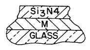
With reference now to the drawings, Figures lA and 1B
illustrate one particular type of heat treatable layer
system contemplated herein_ In these two figures, a nickel
containing metal "M" virtually free of any oxidation or
nitride has been formed by sputter coating (e.g. to a
thickness of about 50 to 300 A)_ In Figure lA this
metallic layer is simply overcoated by sputter coating with
Si3N~ (e.g. about 10 to 750 A thick)_ In Figure 1B an
undercoat of Si3N,, was first sputter coated onto the glass
substrate (e.g. to a thickness of about 10 to 750 A).
The layer system of Figure 2A is similar to that of
Figure lA and the layer system of Figure 2B is similar to
that of Figure 1B except that, by the designation "M/O" it
is indicated that an acceptable heat treatable layer system
can be achieved despite the existence of a small amount of
oxidation having been formed in the metallic layer. While
not precisely quantifiable, in certain instances as much as
about 15a oxygen in the sputter-coating gas may be
tolerated and still achieve the desired results of this
invention. The layer thicknesses here are the same as in
Figures lA and 1B respectively.
Figures 3A and 3B show a family of layer systems in
accordance with this invention. Here, whether only
overcoated with Si3N4 (Figure 3A) or in addition,
undercoated as well with Si3N,, (Figure 3B) stoichiometric
26
217652
metal oxide layers MOX surround the substantially metallic
layer M/O.. The layers are sputter coated to the
thicknesses within the guidelines given above.
Figures 4A and 4B illustrate yet another family of
layer systems contemplated by this invention. Here two
layers of metal "M", or slightly oxidized metal "M/O" are
separated, and surrounded by layers of Si3N~. Once again,
the layers are sputter coated to thicknesses within the
guidelines given above_
Figure 6 is a combined hybrid of the families of
Figures 3A,B and 4A, B, in that here there are two metallic
layers M/O, each surrounded by stoichiometric oxide layers
MOX which in turn are surrounded by three layers, Si3N,,.
Again the layers are sputter coated to thicknesses within
the guidelines given above.
Figures 5A and 5B set forth another family of layer
systems according to this invention. Here the metallic
layer is overcoated (alone, Figure 5A) or optionally
undercoated as well (Figure 5B) with Si3N~ as in the other
families. However, in this embodiment substantially pure
nickel has been admixed with Si3N~ as the separate metal
layer. This intermediate Ni/Si3N~ layer uniquely serves in
certain circumstances to achieve desired solar management
characteristics yet is highly durable, heat treatable, and
abrasion resistant. The weight percent of Ni in the
preferred embodiments is about 80 to 900, the remainder
being Si3N4.
27
2116520
The layer systems of this invention may be formed by any
conventional sputter-coating technique, using for example, a
conventional sputter coater such as an Airco-TemescalTM multi-
zone sputter coater of known design. One preferred way,
however, of forming the coatings of this invention is to use
the unique techniques and targets as disclosed in aforesaid
U.S. Patent No. 5,403,458. Generally speaking, and as
disclosed in this copending application, a. unique sputter-
coated target for producing Si3N9 layers is employed to
overcome the problem of coating the anode with a non-
conductive layer (e.g. of Si3N4). This is accomplished by
uniformly mixing with the Si of the target another element, in
small quantities, which will render the ultimate layer formed
(and thus the layer formed on the anode) conductive thereby
alleviating the anode reconditioning downtime problem
prevalent in the art.
In the practice of the subject invention where heat
treatability, solar management, durability and abrasion
resistance are desired characteristics in the layer system,
care must be taken in choosing the conductive element to be
admixed with the Si in the target so as not to defeat, in the
ultimate Si3N4 layer formed, its purposes and characteristics.
Thus, in the practice of this invention it is preferred for
most systems contemplated that the
28
2116520
conductive element used will be limited to small amounts,
usually less tran abut 10 o and preferably less than aboi,,L
5°s. Such elements furthermore should generally be highly
resistant to oxidation. Metals such as gold, platinum and
nickel may be employed. Preferred, however, for most
purposes contemplated herein are the metals titanium,
zirconium, chromium, hafnium, and mixtures thereof. These
elements are preferred because they generally form nitrides
which are electrically conductive and, optically as well as
mechanically, do not interfere (and are compatible with)
the primary material Si3N~. To the extent they form
nitrides, however, the amount of such a nitride formed is
to be minimized. To the extent that any silicide is formed
of these metals it is believed that it is an intermediate
which quickly breaks down into its respective nitrides, but
in any event is compatible with and does not optically or
mechanically interfere with the Si3N,, is any event, to the
extent that it may remain.
A particularly preferred target for use herein is an
Si target doped with about 5o titanium_ It has been found
that the resultant layers) formed (e. g_ the Si3N~
illustrated in Figures 1-6) comprise (s) about 95o Si3N,,, the
remainder being titanium nitride. This small amount of
titanium nitride has been found not to interfere materially
with the optical, mechanical, chemical, color or heat
treatable characteristics desired i.n the practice of this
invention. In like manner, furthermore, the nitride of
29
2176520
zirconium, chromium or hafnium can also be tolerated for
the purposes cf achieving production efficiency in
approximately the same amounts.
This invention will now be described with respect to
certain examples thereof.
EXAMPLES 2.17 6 5 2 0
The following layer systems were sputter coated onto
clear glass substrates using Si target(s) (doped with 5%
aluminum) and conventional sputter coating techniques as
indicated. The chemical and durability tests employed are as
described above. The heat treatment employed exemplified a
typical tempering process by subjecting th.e sample to 1265°F
(685°C) for 5 minutes. Heat treatment samples were either 3"
x 3" or 4" x 4" squares.
EXAMPLE 1 (Prior Art Exemplar)
A layer system of a prior art exemplar such as falls
within the scope of our aforesaid U.S. Patent No. 5,229,194,
was formed by sputter coating. The layer system so formed
from glass outward was Sn02/Mox/M/O/MOx/Sn02 wherein M = Haynes
214TM Alloy. The product showed excellent heat treatability
and an RS of 79 ohms/sq. However, it failed the chemical
resistance test (i.e. 5% HCl boil at 220°F for 1 hour) before
heat treatment at 5 minutes and at 12 minutes after heat
treatment. The Taber abrasion test was passed in that there
was a 7.6% change in transmission prior to heat treatment at
300 revolutions, but only a 1.2% change in transmission after
heat treatment at 300 revolutions. This evidenced quite
acceptable mechanical durability characteristics. Despite its
somewhat low chemical resistance as determined by the boil
test, this prior art coating system has proven to be an
excellent heat
31
2176520
treatable coating for many applications where very reduced
visiblE transmission is require3, and this kind of chemical
resistant is of little or no concern. An example of such
use is in "privacy" windows in automobiles. In this
respect visible transmittance of this prior art exemplary
is about 23~.
EXAMPLES 2-24
A series of layered films was now made for comparison
purposes using standard sputter coating techniques and
thicknesses within the above guidelines_ The results are
as follows:
32
2176520
Example Heat Acid
.
No. Layer System Treatment Boil
2 SN02/2140X/214-0/2140X/SNOZ/SigN4 F F
3 SNOZ/2140X/214-0/2140X/Si3N,, P P
4 SN02/140X/214-0/214oX/Si3N~/SNOZ PP
5 Si3N,,/2140X/214-0/2140X/Si3N,, P P
6 SigN,,/214/Si3N~ P P
7 SigN~/214-N/Si3N~ P F
8 Si3N~/214-N/Si3N,, P F
9 Si3N,,/214-N/Si3N,, P F
10 Si3N~/214/Si3N~ P P
11 Si3N4/2140X/214-0/2140X/Si3N~**
12 Si3N4/214/Si3Ni/214/Si3N,, PP
13 Si3N,,/214/Si3N,,/214/Si3N,, pP
14 Si3N~/2140X/214-0/2140X/Si3N~/2140X/
214-0/2i40X/Si3N~ p P
15 Si3N,,/2140X/214-0/2140X/Si3N~/2140X/
214-0/2140X/Si3N,, P p
16 Si3N4/214-OJSi3N~ p P
17 ***SigN~/Ni/SigN~ p P
18 SigN4/Ni/Si3N~/Ni/Si3N~ P P
19 Si3N~/Ni/Si3N~/Ni/Si3N,, P P
20 SigN4/SS-316/Si3N,, P -
21 Si3N4/SS-316/SNOZ F -
22 Si3N,,/(80/20)/Si3N,, p P
23 ****Si3N4/(80/20)-0/Si3N4 P P
24 Si3N,,/(80/20)-0/Si3N,, P P
*p - Passed test
*PP = Passed test both before and heat treatment
after
3 *F - Failed test
0
**This layer system was tested the Taber both before
and passed test
and after heat treatment
* **This layer system exhibited low ce characteristics
emittan
(En=17)
3 ** **80/20 is an alloy of 80$ Ni and by weight
5 20$ Cr
33
2176520
Examples 22-24 in the above table (reported here as
2A, B, C) were formed in the following way on an ILS-1600
Airco sputter coater using 5/32" clear glass. The
following conditions were employed:
Line Film Base GAS GAS
1: 2:
Ar N2
(02)
No. Layer Pressure
IG Flow Cap. Flow Cap.
(sccm) Mono. (sccm) Mono.
1 Si3DI~ 4.1x10 25 5.5x10 25 8.8x10-'
6 '
2A 80/20 2.0x10⁻⁶ 40 6.9x10-''
2B 80/20-0 1.5x10⁻⁶ 40 7.1.x10-43 (02) 7.5x10-~
2C 80/20-0 2.0x10⁻⁶ 40 7.1.x10 6 (02) 7.8x10
'' '
3 Si3N,, 2.5x10 25 5/8x1- 1 25 I 9.0x10-'
6 '
Line Film Drive Cathode Volt- Sput-
Parameters
No- Layer Motor age ter
Speed Under Pres-
Voltage Power DC Cath- sure
Power Load KW AMPS ode IG 1
Level Lock
1 Si 35x16 7 _ 420 2.9 7.0 424 5. Sx
N4 0 -'
2 0 3 10
2A 80/20 35x2 8.5 473 4.0 8.7 477 S.Ox
.
'
10
2B 80/20 35x2 8.5 486 4.2 8.7 490 5.3x
-
-0 '
10
2C 80/20 35x2 8.5 501 4.2 8.7 503 S.Ox
-
-0 '
10
3 Si3N, 35x8 7.0 424 2.9 ?.0 426 5.7x
'
, 10
Example 24 had an Er, (at 10 microns) before heat
treatment of 0.34 and an RS of 58.1. After heat treatment
the RS was 28.0 and the E~ was 0.23. Illuminant C 2°
observer values before and after heat treatment were as
follows.
34
2176520
Before heat
treatment:
TY 19.42 RGY 16.11 RFY 34.48
x .2873 x .3259 x .3459
y .2967 y .3255 y .3556
a 24 a -1.87 a -0.96
-1
b . b -3.53 b +15.11
-6.77
After heat
treatment:
TY 26.28 RGY 12.61 RF'Y 28.36
x .2869 x .3209 x .3558
Y -2986 y .3173 y .3641
17 a +2.58 a -0.41
-2
a . b +1.19 b +17.54
b -7.04
All three products were found to be heat treatable,
durable and chemically resistant.
Example 17 in the above table was formed in a similar
fashion using 5/32" clear glass with slight variations in
operating conditions as indicated below so as to make up
three samples a, b, c. The sputtering of the Ni layer
included a startup with 10% 02 with heatup for 10 minutes,
then shutoff. All samples were heat treatable, chemically
resistant and durable. The operating conditions were as
follows:
Line Film Base GAS GAS
1: 2:
Ar NZ
No_ Layer Pressure
Flow Cap. Flow Cap.
(sccm) Mono. (scan) Mono.
1 Si3N~ 7.8x10 25 4.8x10 25 7.1x10
6 ~ ''
2a Ni 6.0x10⁻⁶ 80 1.6x10⁻³
4x10⁻⁶ 80 1.6x10⁻³
8
2b Ni .
2x10⁻⁶ 80 1.6x10⁻³
2
2c Ni .
Si 8.4x10⁻⁶ 25 5.4x10-''( 25 I 8.2x10
N ''
3
4
2176520
Line Film Drive Cathode Volt- Sput-
No. Layer Motor Parameters age ter
Speea Under Pres-
Power Voltage Power DC Catk:-sure
Load KW AMPS ode IG 1
Level Lock
1 Si3N4 35x16 7.0 422 2.9 7.0 425 4.5x
10-~
2a Ni 35x1 8.5 562 5.3 9.5 564 8.8x
l0
2b Ni 35x2 6.0 543 3.8 7.0 545 8_9x
10-''
2c Ni 35x2 7.0 547 4.1 7.5 550 7_5x
1 O-''
3 si3N4 35x8 7.0 429 2.9 7.0 428 4.3x
l0 ''
For Example 17, sample C, the illuminant C 2° obs.
values were determined both before and after heat treatment
and were reported as follows:
Before heat treatment:
TY 23.48 RGY 12.74 RFY 31.94
x .2847 x .3369 x .3418
y .2948 y _33444 y .3499
a -1.56 a -2.27 a -0.47
b -7.97 b +6.02 b +12.77
After heat treatment:
TY 22.44 RGY 14.45 RFY 32.41
x .2835 x .3370 x .3390
y .2932 y .3367 y .3461
a -1.41 a +1.78 a -0.17
b -8.37 b +6.72 b +11.48
Sheet resistance RS before heat treatment was 23.5 and
after heat treatment was 17Ø Normal emittance (En) before
heat treatment was 0.24 and after heat treatment. was 0.17.
Example 17 was heat treatable, durable and chemically
resistant_
36
2176520
With reference now to Example 11, in the above table,
an 8"x8" sample of 5/32" thick clear glass was formed by
the sputter coater under the following conditions:
37
2176520
~ S
S S S
S J S ~ 1
1 S"~
1 1 O 41 O O O O
O O ~
.-r.~ +~ .-i.-r
m
. X X X +~ X X x X
O m
H
N V' M ~ M ~O O~ tD
N
'
10 . . . p.
O 1-a
(
J
(!] In M M M
N (ZI
H
O
d)
_ (J1
'LS
M E
3 ~
O U
~
U O u~ o wn
m O .
U -~
'
.--a O O
m '
C~ GI. v M d a V' M V w
v ~ 1
U
i i
O O
. X x v7
Q 0. O O 1 O O
O O .
1a ' U
O
U ao ao A ~~ c~ a~
~
N
z
N E
U
O 3 o v o~ ~ o
ti
m W o O
3
Id .--~ N IL M N M N M
m ~G
N
m
,' la
O O O O O
~i .-~O .--~,1 a~ ro
o x x
.-,x x O ~~ox
n. ~ v x v N E .--~ <n M ~ N o
G ro
v
ro ~' ro O cV M N M ~)
O O
O
v' .-..a .-,c' ~ > r c-uc M v
.-7
a
a~ a
'O
r, E O 3
~
3 ~ o
v a~
m O 1~ f~ O O ~ O O
U >
ro .-a It1O O O ~ ro ~
m
U' (y N .-1V' f-1N U dP f~ f~ O~ f~f
" ~7
~ ,o,o .o .o
1 dP
-a
O O O O
m O .-~.~ .-i~ Ul ID
S
yO
N .~ X X X x > ~~ N N N o~
m O
H O
m X M ~p ~ N .-~ x x x x x
a~ ~
a~
ro N 11 m u m InIn
it O
C~ O.
W M .-1N .--1t'~ D n"7l'1t'~M M
L11 ~
N ~
x o x s~ x o x
'
Ear z' o ~ o z E' z o ~ o z
.-a ~ ~ c v
?,
_a -a .~.--m, -.a .a .a .-~.~ .,-a
ro ro
(x, f/7N N N ~ W V7 N N N V7
,~ 1-a
d7
C C
.
O -.-1
O '
.-1N M ~' U W -] .-iN M C W
Z
38
2176520
Sheet resistance before heat treatment was 82.6 and
after heat treatment was 46.1. Normal emittance (E~) before
heat treatment was 0.48 and after heat treatment was 0.33.
Before and after I11. C 2° observer data was reported as
follows:
Before heat treatment:
TY 26.04 RGY 12.29 RFY 29.27
x .2869 x .3319 x .3436
y .2958 y .3327 y .3527
a -1.17 a +1.40 a -0.74
b -7.-76 b +5.15 b +13.30
After heat treatment.
TY 28.34 RGY 11.54 RFY 26.69
x .2895 x .3321 x _3395
, y .2988 y .3341 y .3472
a -1.34 a +1.09 .a -0.31
b -6.88 b +5.32 b +11.09
The Taber test prior to heat treatment showed a change
of 7.6%. After heat treatment the change was only 1.20.
The product produced was heat treatable, durable and
chemically resistant.
Examples 12 and 13, from the above table, were formed
in a similar fashion and showed superior heat treatability
characteristics and excellent chemical resistance. Example
12 was dark and Example 13 was not. The operating
conditions were as follows-
39
2116520
O O O
. x x x
o
, O O N
G
s0
O
a0 0o ao
N
z
N E
3
U
W O
U
.-1 ~ U7
m
(x, N N N
~
s
O O i O
O O
.-1ri.-1.-1r-1
. X X X X X
O
f~ O ~D ~ O
1
N
O
U t vOW O m
y
1a
3
U
tA O
U
p 0 .-r tn O X11O m
m
(x, N C'N V N
~
U1 ,o ,o,o ,o
1a n
O O O O O
m
O X X X X X
f0
H
(J~ W V ~D(~ r-1CO
O
C17 c7 r1.-i.-1O~
P,
H
la
x z
z
w .--y, ,c, c,
~
.., -..~~ -. .-,-a
~e
(z, V7 N f11N tn
,..]
O
N
C i
~
a -a
O
.--1N ~'~1C' 1f7
2176520
,
,
0 , , , , , 0
0 0 0 0 0
x x x x x x
o , .n a.
o
ao ~ .
a,
~ v c~ v v ch v v
c~ c v
~n
a.
r~
a~
a~
rn
~
~a~o
~
d~ 1 Q~ d'
.-1 N ' t~ M a' f~ r1
'd
1~
O M O r~ r~ v
C
,d
~ v ~r ch ~
~
U
p Vw D O
q Iw D V' tw D Q' f
1~
N
O v0 a0 O v0 aD O
N ~ M N .-1M N '-1(~
x
-J
1~
U m
U W N
~ U~
m
a~ ~~x
r-1 O tD t0 ~ c0 ~D
,d
U
,0 O <'~o~ c~ M o~ t~ M
O
O
>a.~ ~ M M ~ M
m
,o w
a O 3
-~
m ,c O
a~ O O ~ O O t"7O
(1 ~
~
y , -
O
U da c mn a~ m n c~ ~
.7
,o
t~
C
m
dP
N
Q)
1WLJ CO
.1 N N OJ N N
x x x x x x x
S.r ,n ,n u, ~r W W
o n
~.
O M M c-7M M M M
~
tn
M
I
'O
C
~
z ~r v c~ v
N -.-I .-1.-1 .--1--J .--1r.-1-.J
IU
(/]N N (n N N V7
m
N
a
a m a m
.-1N N M V C' tn
x
m
QI
2176520
EXAMPLE 25
A coated glass article useful for architec:ural or
automotive purpose was formed on a production sputter
coater using a typical 5/32" float glass and Haynes 214 as
the metal "M". Figure 1B represents the resultant layer
system wherein the Si3N~ undercoat was approximately 550 A
thick, the Haynes 214 layer was approximately 100 A thick
and the Si3N4 overcoat was approximately 275 A thick. A
conventional Airco (Solar Products)-Temescal Multi-Zone
Architectural Sputter Coater as illu~~trated in Figure 7 was
employed, and whose various parts are described in more
detail in Example 26 below. The operating conditions were
as follows:
42
2176520
Coat ZoneCathode Material Volts Amps P (KW)
~
1 Si 417 60.7 25.3
2 Si 428 97.7 41.8
3 Si 412 97.0 40.0
1 4 Si 419 69.8 29.2
5 Si 409 90.0 36.8
6 Si 448 92.9 41.6
7 Si 415 70.7 29.3
g Si 417 42.5 17.7
g Si 431 86.3 37.2
2 10 Si 416 81_6 33.9
11 Si 420 86.3 36.2
12 Si 430 90.4 38.8
31 214 469 36.9 17.3
3 32 214 462 36.7 17.0
33 2i4 463 36.1 16.7
4 19 214 426 18_9 8.1
25 Si 402 30.9 32.4
26 Si 433 66.1 28.6
27 Si 410 75.1 30.8
5 2g Si 418 49.9 20.9
29 Si 452 70.8 32.0
30 Si 424 71.3 30.2
43
2176520
ZONL; 1
Gases Argon and nitrogen
Gas Ratio 80o N2; 20% Ar
Gas Flows 1448 N2, 365 Ar
Throttles 10%
Flow Ratio A B C D E
21 29 0 29 21 ( a )
Pressure 2 . OxlO-3 Tor r
ZONE 2
Gases Argon and nitrogen
Gas Ratio 80o N2; 20% Ar
Gas Flows 1856 N2, 433 Ar
Throttles 9%
Flow Ratio A B C D E
24 26 0 26 24 (%)
Pressure 2.1x10³ Torr
ZONES 3 AND 4_
Gases Argon (1000)
Gas Flow 1821 scan Ar
Throttles l~~
Flow Ratio A B C D E
20 20 20 20 20 ( o)
Pressure 2.0-2.1x10⁻³ Torr
ZONE 5
Gases Argon and nitrogen
Gas Ratio 80% N2; 20% Ar
Gas Flows 1421 NZ, 312 Ar
Throttles 140
Flow Ratio A B C D E
19 31 0 31 i9 ( o)
Pressure 2.2x10³ Torr
The resultant product
was tested and the
results are
reported as follows:
44
2176520
I. (a) visible transmittance (I11.C 2 observer):
before heat treatment ~3~
after heat treatment 22%
(b) reflectance:
before heat treatment
glass side: ~15-16%
film side: ~22-240
after heat treatment
glass side. .~=14-15 0
film side: .~17-180
(c) emittance (F.~,)
before heat treatment 0_50
after heat treatment 0.55
(d) sheet resistance (ohms per sq.):
before heat treatment 60.0
after heat treatment 73_5
II. Durability test only)
(mechanical)
(Taber
before heat treatment 8-9~
after heat treatment 5-60
III. Chemical resistance (boil test)
j before heat treatment pass
after heat treatment pass
217620
EXAMPLE 26
A conventional Airco (Solar Products) TemescalTM multi-
zone architectural sputter-coater of known. design is used.
This coater is schematically illustrated in Figure 7. In
Coating Zones 1, 2, 4 and 5 there are employed three cathodes,
each with two rotatable targets. In Coating Zone #3 there are
employed three cathodes, each with one planar target. Thus
the resulting targets are 1-27 (e. g. Coating Zone #1, Cathode
Bay #1, Target "1") Glass substrate G, herein shown as a flat
glass sheet (e. g. in the shape of a flat, yet to be bent
and/or tempered part) is conveyed on a roller through the
AircoTM sputter-coater whose zones are separated in a known
fashion by walls (F) having in their lower extremity an
adjustable tunnel (T). Pre-wash (W1) and post-wash (W2) are
conventionally provided.
Using this equipment the layer system of Figure 1B was
formed, wherein metal "M" is a substantially pure metallic
nickel/chromium alloy (80/20% by wt. Ni:Cr). All 12 targets
in Coating Zones #1 and #2 are of the same metal (e. g. silicon
doped with about 5% A1) from which a silicon nitride layer was
formed. In this case, Zone 1 and Zone 2 were regulated to
approximately 2-3 microns (2-3x10-' Torr) with an 80% NZ and 20%
Argon atmosphere. As Glass G progressed through Zones #1 and
#2 at the aforesaid pressure, silicon nitride was applied to
the glass as layer "A" to a thickness of approximately 500A.
46
3.
2176520
As glass (G) progresses into Coating Zone #3, cathodes
7, 8 and 9 sputter a layer of the pure metallic nickel
chrome alloy (80-20) in Argon at a pressure of 1-2 microns
(1-2x10⁻³ Torr). The thickness achieved was approximately
150A.
Glass (G) was then moved through Coating Zone #4,
which was regulated to a pressure of about 2-3 microns (2-
3x10⁻³ Torr) with an 80% NZ and 20 o Ar atmosphere. Cathodes
10, 11 and 12 (six metallic silicon targets) were used to
apply a layer of silicon nitride. The glass was then moved
through Coating Zone #5, which was also regulated to a
pressure of approximately 2-3 microns (2-3x10⁻³ Torr) with
an 80% NZ and 20o Ar atmosphere_ To apply further silicon
nitride, a total of six targets are used in this coat zone.
A11 silicon targets were 95% Si, 5o Al, by weight. The
total thickness of the overcoat layer of Si3N,, created in
Zones 4 and 5 was approximately 300A. This then completes
the heat treatable coating system.
The process conditions are as follows:
47
2176520
r.,
--a p p o 0 0 0 0 0 0
~
0 0
N N \ \ ~ ~ ~ \ \ \ \
N
O O O O O O O O
rd N O ao ao ao co ao m m
O O
O
~ z m ao
Qo
0o
ao
a
a '~ '~ ~ 0 0 ' ' 0 0 0 0 0'
0 0 0
-.
0 0 ., .~ ~, ~, .~ r, .
s x x x x x x x x x s~
~ ~ a a l~ a a ~
m x x x ~ .-~ .-r o o o o o o ~
s~ ~. ~ a s~ ~ i~ s~ s~ ~
~ ,~ ,~ r, .o ,o ,o . .o .o .o o
a ~ a
.o o o .o N N N N N N N N H
H H H H H H H
N N N
H H H
~d
la
O
J-~ ~ -,~ _.a -.-1-.a -.-1-.-1-.a -.-1
a
rd -a --a " N
GO
a1 O~ Q~ O a7
O O dw D of t~ c~7
p N O X X v0 c~ c- 00 rn o~
,n .~
4J
'O
O w
.C J- W D (~ O~ N .1 O~
O
.-i N ~ O d. .-1 N V'
-1 O O O
x X r~ v c a d
v
m o0 0 ~o
co ~o m
~y. .n a~ v .a
N X X N ('1 t~ t'7 V' d'
a( ('~ .--1N
J-~
O
1r
v ~ t''1d' ~f7 tD
H
N N V r-1 N
N
.b
O
U N ('~ t'7 d' d' ~f7 U W ~D
D
r1 .-1 N
N
C
N
N
2176520
c c o 0 0 0 0 0
O dP dP dP N N N N N N
O O O \
\ O O O \ \ \ \ \ O
y~ O' ~T LP O
dp
,0 O O O O O O O w
N f-1 11 11
~ z r, .i i w ao ao ao ao
st .t ~s
s, , , ,
0 0 0 0 0 0
0 0 0
m r, ~. r. r, .-~ .-. .-~ ~, r,
m x x x x x x x x x
s. a s. a ~ ~ ~ ~ ~
,n ,n ~n r, .-~ r. .1 ., ~
sa a 1a 5a a 5r sa sr sr
,o .o .o .o .o .o .o .o .o
p, .~ 1 .1 N N N N N N
H H H H H H H H H
~r
-a
i, -a -.a -.r
i, s.~ 1,
N Z Z Z
U U U
t~
N O O O --r -~ -'a
O O O
QO N d0 tJl (l7 (ll (n tn V7
N N N
t17 d' CO O O uW D u7 a'
tf1 ,17 V' .-1 O O~ O~ O~ O
N N N Q' d' ~ fh N d'
QJ
Om
-C
i~ 1p N O O O~ '~ ~ N
,6 ,.,7u~ ~ ,--1.1 O '-1 O O
O
U ~ <r v e' v v' ~ v ~ v
.-1 r1 O~ C' N N ~ .-1 V'
3 .~ . o ao co c~ c~ ~ co
~
a~
'-i N M .1 N (7 V' IW O
'b
O
p p .-1 .--1N N
U c~ co a~
O
N
99
2116520
o 0 0 0 0 0
N N N N N N
\ \ \
0 0 0
ro o 0 0
N
~ z ao m ao ao ao ao
a~
, , , , ,
0 0 0 0 0 0
s x x x x
~ ~ s~
o, x x Nu N11 N1-~ N11
Nu ~
N11
a . a . . .
O O O O
f1 Ni N (~k N N N
H N H H
r-1
ro
N
J-~
-.J -.-1..~i-.1 -.-i -.J
Ql ~D c'7 tD N N V'
C~.L ~O tn V ~f1 tf1
' Q' d V
N
'Z7
O m
10 vD d' d'
td ~ O O~ O~ .-1 d'
O
U ~
~ u7 ~
o a o, v, o~ N
.-1
a~
ro
N ~ c. ~n
N
'O
O
ro ,., M ~! c mn u,
Q1
C
O
N
2116520
Line Speed: 200"/mn
Glass thickness and type: 3.9 mm green tint
The resultant optical characteristics are:
Optics as coated I11_ "C" 2° obs.
TY 22.65 RGY 16.02 RFY 22.43
a* -4.53 a* -2.51 a* +1.21
b* -8.82 b* -0.45 b'* +27.12
Sheet resist. - 65.3 ohms/sq.
Normal emit. - 0.50
Optics after heat treating* I11. "C'! 2° obs.
TY 23.04 RGY 15.37 RFY 23.46
a* -4.07 a* -3.52 a* +0.04
b* -7.13 b* +1.15 b* +22.15
Sheet resist. - 47.3 ohms/sq_
Normal emit. - 0.45
eT +0.39 eRG -0.65 eRF +1_03
eE 1.87 vE 1.09 eE 5_90
eSheet resist. - -18.0 ohms/sq.
eNormal emit. - -0.05
Testing
Chemical resistance:
As coated - No change in physical properties
after boiling (230°F) in 5o HCl
acid for one hour
After heating - no change .in physical properties
after boiling (230°F) in 5% HCl
acid for one hour
Taber abrasion test: eT (transmission) @ 300 cycles and 500
gram load
As coated - eT = 8.1%
After heating - eT = 6.30
*(heat treating was @ 665°C cycled for an automated time
period of 16 minutes)
57
2176520
EXAMPLE 27
This example was formed on the equipment as described
in Example 26 above. The same cathode, target gas ratios,
pressures and process conditions were maintained as in
Example 26 in Coating Zones #1 and #2 to achieve an
undercoat of Si3N~ (and some aluminum nitride from dopant)
of the same thickness as in Example 26. Changes were made,
however, to the process conditions in Coating Zones #3, #4
and #5.
The gas composition in Coating Zone #3 was changed
from 100 o Argon to a 95 o Argon, S% oxygen atmosphere at the
same pressure, and power was increased to the targets in
Coating Zone #3 to give a metallic layer on glass (G)
j similar in thickness to that of Example 26. The layer
system formed was that of Figure 2B where M was the same
Ni/Cr alloy as used in Example 26, but here partially
oxidized. The glass was passed through Coating Zones #4
and #5 where, as before, a silicon nitride layer was formed
on top of the metallic, now partially oxidized layer (M/O).
This topcoat of Si3N,, was kept somewhat thinner than in
Example 26 in order to more nearly match the desirable
optics of Example 26. The advantage of the coating layer
system in this example over Example 26 is that the sheet
resistance (and normal emittance) of the product. after heat
treatment actually achieved, is in the range of typical
"low-E" coatings. Thus, this coating layer system has the
ability to reflect more infrared energy as compared to the
52
2176520
coating layer system in Example 26. Chemical durability is
reduced only slightly compared to Example 26, but
mechanical durability is improved over Example 26's already
good durability.
The process conditions are as follows:
53
2176520
0 0 ~ o
000 ~ ~ , ,,
~ ~
N N N \ \ \ \ \ \ \
N
\ \ \ \
\ O O O O O O O
O O O O m oo ao ao 0o co co
O
~ z 0o co
ao
ao
ao
a~
0 0 0 0
0 0 0 0 0 0
a o 0 ~ r, .~ .-~ ~ .-, .~ ~~ .-r
m x x x , x x x x x x x x
~ ~ a ~ s~ ~ s~ a ~
m a s~ ~ x -~ .-, o o o o o o
s ~. ~ a ~ ~ s~ s~
.., ,~ ,.i . ,o ,o -o .o o -o o
~ a ~ ~
. ~o ~o ~o ~o N N N N N N N
E-. H H H H H H
Er H H N N
H H
ccf
1r
a
_a -r -a -..~_.r _.~ ..r -.
a
m ., ..r -.
i
O d r r co
m o~ O d r
. . . . O in r o7 r
~ ~ ~ x x .n r ~ m a, 00
m
om
~ .-1 d ~"1 O~ ~ ~ N U7 N f'7 ~t1
~d N
O X V' d d d C d
U 7 d d d d X
N u1 a0 O W d
d ~ r N
~ ~ X N t'7 r'1 d d cf
x N N X
1~
1~
N d ~ ~ ~ N N y f1 ~9
E, .-1 N
p
1~
N N t'7 t'7 d c Wf1 ~ tD vD
U
.-1 .-a
CJ
C
p N
H ~
54
2176520
~ x o 0 0 0 0 0
sr
x x O N N N N N N
r ~
O
EC
O \ \ \ \ \ \
~
N /n tn O O O O O O
u7 u1
,~ ~ a oo ao 0o ao ao ao
~ z o. a
w
a~
0 0 0 0 0 0 0 0 0
~ ,~ r, .~ r, ~-, r. .-, .-
m x x x x x x x x x ~
m ~ ~ ~ a ~ ~ ~ a
a u, ~n o o o o o o a
a s~ s~ ~ ~ ~ s~
o ,t, o .o .o .o .o .o .o
.o .o , N N N N N N H
- H H H H H
w ~ ~ r
H H H
ro
y, -a ..~ -.a
y~ a ~
N z z z
U U U
O O O
O O O .,.i..~ -.a V
(D ~ CO (f7 (/l (n (n ul 7
N N N
m O~ ~ .1 h v0 ~-1 .-i V' N
.
r ~p ~p t0 ~D r
' ~ ('7 N N N N N N
t
7
O
O m
--1 OJ O~ O~ CO O N d
uW . vD O O O .--i.--~O
0
ro d d V d d d d d
.O~
d
.--rr~ m O < ~
N N .-i ~-i N N
ro
<W "7 ~ N tv7 d tW D
N
O
O O ,~ rl N N
ro ~ ~ O~ ,1 r r-1 ~-1 r-A r-1
1
(
O
C
O
2176520
0 0 0 0 0
0 N N N N N
\ N \ \ \ \ \
\
yJ O O O O O O
rd
N
~ z w ao m o~ co ao
0 0 0 0 0 0
~,
m x x x x x x
s~ a ~ ~ ~
r, ~ r, .~ ~, .,
i., s~ s~ a s~ s~
.o .o .o .o .o .o
N N N N N N H
H H E-, H H
1~
d7
a~
.a
v1 v7 cn m cn cn
U7 ~ r cW O o~ 00
r ,o ~ .o .~ .fl
N N N N N N
N
17
Q
--1 O N O N
1) N . O~ Q~ ri ~'
.-i CO O
c0
O
U ~ c-7 C' c-~ c-7 v v'
r1 d' f7 1n U7 N
~, .-~ .-, r~
x ~ ~ ~,
a~
N M .~. y D
d7
'O
O
ch r1 V V uI1 ~
U .~ .~ ~ .~ r, ~
C
O
J E7
2176520
The optical results achieved were as follows:
O tics as coated Iil. "C" 2° obs.
TY 18.70 RGY 12.76 RFY 25.12
a* -5.06 a* -0.43 a* +0_40
b* -1.04 b* -4.27 b* +24_56
Sheet resist. - 104.5 ohms/sq.
Normal emit. - 0.55
Optics after heat treatincr* Ill. "C" 2° obs.
TY 23.59 RGY 10.77 RFY 21.61
a* -5.46 a* -0.36 a* +206577
b* -3.47 b* -4.84 b
Sheet resist. - 15.2 ohms/sq.
Normal emit. - 0.183
eT +4.89 eRG -1.99 eRF -3.51
eE 6.03 eE 3.45 eE 4.74
eSheet resist. - -89.3 ohms/sq.
eNormal emit. - -0.37
1
7
Testing
Chemical resistance.
As coated - slight change in physical
properties after boiling (230°F)
in 5o HC1 acid for one hour
After heating - slight change in physical
properties after boiling (230°F)
in 5o HCl acid for one hour
Taber abrasion test: eT (transmission) @.300 cycles and 500
gram load
As coated - eT = 3.10
After heating - ~T = 1.80
57
2116520
Once given the above disclosure many other features,
modificatons and improvements will become apparent to the
skilled artisan. Such other features, modifications and
improvements are therefore considered to be a part of this
invention, the scope of which is to be determined by the
following claims.
58