Note: Descriptions are shown in the official language in which they were submitted.
21 76638
SEGMENTED SHIELDING STRUCTURE FOR CONNECTOR PANELS
Cross-R~relei~ce to Related Application
This application is a continuation-in-part of copending application no. 08/415,627, filed
April 3, 1995.
Back~ ulld of the Invention
1. Field of the Invention
The invention relates to the field of ele l o~ gn~tir ~hi-oldin~ via CG~ uCIi-~ gaskets that
bridge across Opel~hl~,S bel~n~n parts of c~n~ ctive housings. Accold.~ to the invention the
~hiPl~1in~ U;lUl., is defined by a pluMlity of resilient co~ clivt:ly w.~d segm~nt~,
el~ically coupled together by conductive tape or the like to form a gasket. The invention is
particularly useful for shielding relatively large areas such as bypass panels at which
input/output lines ~a~ the boundary of a ~hiPIded enrlQsllre, typically via cQ~ . The
seg...~.t~l structure is such that the col~luelivt: path from a given point on the panel to a given
point on the huusillg or other ground point, is shorter and/or lower in le~ r~ than in a non-
15 seg...~l.lrd all~n~ 1, which improves ~hi~l~lin~ errlc;en~y as colllpaled to a similar gasket
that is continuous rather than segn~
2. Prior Art
To reduce problems due to al~ ;..g ele.;~lo.n~gn~tir fields e ~ n~l;ng from ele~;ll.~nic
c~ and/or due to the l~nf~ y for inrident eleello...aE.~I;r fields to affect se~ ive
circuits, a conductive barrier or shield is placed along the path of field propagation to provide
a discolllillui~. The conductive barrier typically is coupled electrir~lly to a circuit ground.
Part of the elecll~ tir energy inri-lent on the shield is reflPct~d, and part of the energy
induces Cull~ in the shield. These cullelll:i are ~ ^ l as eddy ;u~ . The field is
All~ ted by the shield.
Conventional .~hi~l~lin~ typically uses the external hou~sillg of an article of ele~ onic
e~;l.n~n~ for at least part of the shield barrier. In addition, int~rn~l shield bo~ 7, enclosures,
ground planes and the like can be provided for particular circuit elem~nt~ within the enrlosllre.
For these purposes, sheet metal materials, l~...in~tes of metal and plastic and/or con~ clive
co~ g~ typically form the conductive elecl..).n~gn~tir shield barrier.
Many m5xhorn electronic devices emit or are sel~ilivt; to ele~ gnrtir, ill~,Ç~ ce or
"EMI" at high frequPnri~s. For example, ccillllJulel clock and digital data sign~l~, phase locked
- 21 76638
loops, switched mode power supplies, various radio frequency and miclowave devices and the
like are sources of EMI. Many such electronic circuits also are ~usceplible to EMI, and must
be chi.okl~d in order to operate LJro~lly.
The effecLi~ss of a shield is a ru~clion of a l~ lber of factors in- l~ in~ the electrical
S p,opellies of the shield material (e.g., conductivity and m~gn~tir perm~o~hility), the ~1~;eL~ss
and continuous or discon~ ous nature of the shield, the rl~u.,.~cy of the EMI, the sp~ n~ and
configurations of the EMI source and the shield, etc. For chiPl~ing ç~laLi~ly higher
rl~ P c, any gaps in the conductive material must be smaller to prevent leakage as col~aled
to shiel~lin~ lower freq~nriP~.
The frequenriPs to be ~ include h~--.-o~ s. For a CGl~pu~r, for eA~le,
having a basic clock frequency of 25 to 100 MHz, ci~.;l;r-..l h~....o~ s may be present up to
900 MHz or more. Errcctive chiPl~lin~ lc.luil~,s a nearly corltin~l~us (i.e., gapless) shield,
pl~fc.ably ~lallged cloæ to the source of EMI and/or close to the ~uscey~ible circuit, and made
of a highly conductive material.
Typically, ~hiPl~lin~ is provided by a co~lu~;~ivc enclosure made of thin sheet metal,
mPt~lli7Pcl plastic or the like. An extrrn~l hO"~ can form a conductive chiPlAing enclosure,
and ~hiPl~in~ subenrlos~lres can be provided for ~bzc~ hlies within the l-ol.s;.,~. Err~;livc
.chi.olrlin~ advantageously inr~ es co~ ctivc EMI blockillg gaskets that continue the co~lu~;~ivc
barrier of a shield across any gaps or seams bet~n c-n~ ctive panels, enclosures, doors,
20 hc)u~i,lg cl~-..f-.l~ and the like, which form portions of the shield.
RP~ ntlY col~ ssible con~ ctive gasket structures are disclosed, for c~'^, in USPatents 4,857,668 - Buonanno; 5,045,635 - Kaplo et al.; and 5,202,536 - Buonanno, which are
hereby hlco,~ td. Accor~ g to these patents, a col~lu~;livc sheet md~.ial such as a woven
or unwoven m~t~li7~d plastic fabric is provided on a resilient col~ssible core of indefinite
25 length to form an elongated linear gasket that can be placed bel~ conductive panels to bridge
any gap b~,twcell them, e.g., due to disc0.~ s and the like. One possible conductive
material is Monsanto "Flectron" nickel/copper mPt~lli7lod polyester fabric.
A conductive gasket as desc-ibcd can be formed in various cross seclional shapes,
inrll~ling round, lc~;~n~ular and irregular shapes, and can be provided with an ~ c~ F ~l
30 means such as a clip or an adhesive area, to assist in mollnting. Conductive gaskets can be
made to the specific shape and area needed to reside b~h~ee.l the conductive snrfac~s l~lwccn
21 76638
-
which they are to seal, but it is generally more 1iffi~l~lt and e~l~n~ive to provide cu,lulll~d
shapes and siæs. In addition, conductive gaskets for large sealing areas are more ~liffirl-lt to
make than small area gaskets. As a result, relatively slender linear conductive gaskets or seals
are generally mounted so as to define lines electrically CQ~ ;l-g between conductive panels.
5 Where an O~l~illg is to be provided, the linear seals are allangcd around the pe.il,l~,tel of the
Op~illg.
For a conductive gasket conl~ g a conductive sheet on a resilient core, the core can
be molded, extruded, cut from a block of resilient stock, etc. The conductive sheet can be
wlapped on the core and affiY~ for example, by adhesive. Accor~ing to the above Buonanno
10 pqt~ont~, the core also can colll~lise a polymer with a fOa~ g agent, applied as a liquid to a
woven or non-woven mPtqlli7o-1 fabric that is wlalJped, for example into a closed shape. The
polymer eyp-qnAs to fill the void and as the polymer cures, it engages securely with the fabric.
Providing and wlapping a resilient core can be i~ccQ...l-lished readily for sub~ lly
linear gaskets in round, oval, lc~,Lall~ular or cGlllplcx cross sectional shapes that cover a small
15 surface area. Where the surface area is larger, and particularly where the thir~ss be~
opposite ~ulraces is ...in;...~l, it may be ~iffir~llt to form and/or wrap the gasket in a ~ that
provides an aCCUla~ shape and a smooth conductive CU~li~. On the other hand, slender linear
gaskets are not suitable for all EMI sealing appli~tionc, for example, where a s~ area
of ~bul-n~-l beh ~-l housil~g Clc~ iS to be sealed and/or when the sealed surface is
20 disca~ -olls, for example, to allow cl~ for Co~ ;Lûls.
For larger areas, it would be possib'~ to provide a pattern of linear seals to seal be~wee
the surfaces. Linear seals could be ~,~g~d around the pelil,l~t~ of û~clli~ for COll~
and the like, to allow cle~lce while sealing ~lween the conductive panels. But this is
cumbersome. A ,;~ ollli,~ d wide area gasket with clealallce openings is possible, but this may
25 be l.;ulll~OllR and e~ye~ive to produce.
Another ~iffirlllty with wide area gaskets is that ~ g the colll~ ssible core is not
conductive, then the shol~l conductive path from any point on one side of the gasket to any
point on the o~osi~ side must pass clear across the surfaces on opposite sides of the gasket to
the edge. Th~lerol~" wide gaskets may be chaldct~,l~d by a relatively higher point-to-point
30 lc~ix~ and reduced EMI xhi~l~lin~ errlciellcy as colll~d~ed to a plurality of individual
elongated seals. On the other hand, individual seals are more complicated to mount.
21 76638
What is needed is an improved means for sealing wide areas, having the ease of
mAn If Actl~re of a simple elongated linear seal of preferably regular shape, and the versatility and
wide area covelagf of a more ~;~Lo~ ed shape. Advantageously, such a gasket would also
have a low lesi~livily.
Accor~h~ to the present h~v~lllion, a large area EMI sealing gasket is provided in the
form of a sheet, made by Att~rlling a plurality of laterally a~ Pnt elongated seg....~ using
conductive tape or the like. The sheet can be die cut to size and to provide cle~ ce O pf. ~
inr~ ing openings larger than a segm~ont width. Molw~ ~s the se mPntc as thereby
CO~ provide ~dhion~l and shorter paths ~t~eel1 the sealed surfaces than a cO~ al~bly
10 sized contin~lomc seal or gasket, the shiPlding effirien~y of the shield is in fact mlpl~ved rather
than ~iminichr~, due to its seg.~ r~ form.
S~ A~ ~ of the Invention
It is an object of the invention to provide a lela~ ly wide area EMI shi~lflin~ seal or
gasket that has a high ~hi~l-ling errlrie~y and is easy and in. ~l~n~;ve to ,~A~ rartllre and use.
It is a~so an object of the invention to provide a sheet-like gasket that is readily cut to
form o~.~.,~s providing cleal~ce for col~lle. lol~, circuit card end plates and the like.
It is another object to apply easily m~nllfa~tnred elong~t~ seal structures to sealing over
a wide area that may have a complex confi~-ration, without l~ g attention to placing the
elon~t~ seal ~lluclul~s along edges to be sealed.
It is also an object to provide a versatile seal allang~ l that can a~o.. odate
irregular shapes and surfaces as well as sealing a~ ng~ nlx where conductive -l~lf ~;~l iS to
be placed in sl~cir~c areas and not others.
It is a further object to facilitate acculale mounting and posilio~lg of a sheet-like gasket.
It is a~ r object of the invention to fa~ilit~t~ m~mlf~ me of a se~m~rltPcl seal using
25 effiri~nt means for conductively joining o~osile sides of the gasket along seams l~l~ the
Sf g- - -~
These and other objects are ~cco...plished by an EMI seal or gasket that blocks
elecll~,...agnPtir radiation l~lw~ell e!ectrir~lly conductive bodies and e l~rollll)~cses an area using
a number of ~jacs~t segmPntc, each generally formed as an elongated seal with a resilient core
30 and each pl~ fel~ly being ~IJbs~ lly enclosed by an ele~l. ic~lly conrl~lctive surface for bearing
against the conductive bodies. The se~ i are ~tt~rhP~ to one another along lenglllwise
2 1 76638
seams, preferably using conductive tape on one or both opposite sides of the gasket. The
conductive surface preferably is provided by a m.of~lli7ed fabric affixed to a resilient foamed
polymer core, which can be molded in the fabric or otherwise for ned or cut and ~tt~rh~d. The
fabric can extend s~ lly around the se~ c or be con~luclively joined be~.,en the
S segmPnt~. This stTucture provides more and shorter conductive paths across the gap ~ en
the conductive bodies, as conll)âl. d to a non-segrnrntpd gasket of collll)alable size, lh~leby
improving shiplllin~ efflriPnry. The gasket can be die cut, inrlllAin~ cutting through the width
of one or more segmPnt~, and l.,.llah~s intact. The s~ P~ can be of ulliÇollll or different
shapes, sizes and conductivity. The se~...P-~I~ gasket as desc il~ provides many of the
10 bencr,~ of both wide seals or gaskets h-aving a conAllctive surface material, and elongated
narrow seals, but with improved .~h~ ding errt;clivelless and versatility, and leduced costs.
Brief Desc~iytion of the Dlawhlgs
There are shown in the llawings certain exemplary- e,nboAi...-~ of the invention as
~n,~ll~ly p,~f~.,.,d. It should be understood that the invention is not limited to the e,llbo 1;.. .~-.l~
15 disclosed as examples, and is capable of variation within the scope of the appended claims. In
the dlawhlg~,
FIGURE 1 is a ~-~ecli~re partly sectio~l view ill~ l;..g a seg.~ gasket
accol-iing to the invention, for sealing b~l~n co~Allctive bodies.
FIGURE 2 is a plan view of an exe",l)la,~ se~ d seal or gasket as shown in
20 FIGURE 1.
FIGURE 3 is a perspective view of an e~ l~y housing for an ele-;l,onic device,
wL~eill the gasket seals l~l~,,n the e~t~ l h~-sir~ and circuit card end panels.FIGURE 4 is a section view through a portion of the segmPr~;l gasket according to one
embo limrnt taken along the line of elongation of the segm~nt~, the se~...r..l~ being coupled via
25 a c~n-lllctive tape.
FIGURE 5 is a partial perspective view of a portion of the seglnlonted gasket according
to an ~l~. ..~live embo limPnt and inrludin~ cledlallce o~nillgs, the seg...~ being coupled via
a conductive adhesive.
FIGURE 6 is a partial perspective view showing a fur~er ~ ve embo lim~t,
30 inrludin~ adhesive strips f~rilit~ting mounting of the seg...- n~d gasket.
21 76638
FIGURE 7 illustrates a first al~ ive embodiment wherein the conductive surface
material is joined across the gasket along depressed seam lines.
FIGURE 8 illustrates a further embo lim~nt similar to FIGURE 7, in which the depressed
seam lines are provided on opposite sides.
S FIGURE 9a shows an embodiment wlle~hl the seam lines are formed by depressions on
both sides of the gasket.
FIGURE 9b shows an embolim~t wLe.~ the core se~.. l~ are lapped, thereby
Orr~~ the openill~s on o~osilc sides of the gasket.
FIGURE 9c shows an embodiment wlle.~,hl ndjac~nt seg...~ n~ are ~tt~ched by a zigzag
10 stitch clvs~i~g be~,en ~ ~nt seg.~ nl~
FIGURE 10 shows a further embodiment wl,e.~ a conductive adhesive is provided
b~lwæn core seg-..f-.l!i wla~ed cQ~ o~ly with a conductive sheet material, forming flat or
relatively flat surfaces on bo~ sides of the gasket.
FIGURE 11 shows a further e~llbod ~ having conductive f~lc~f~ in the form of
15 con~luclivc staples or stitt~h~s, cleclrically coupling bcl~.,.,n the segments across opposile faces
of the gasket.
FIGURES 12a through 12f illn$tr~ a series of t~cllniq~es for dealing with the
con.l~ctive sheet material along an edge of the gasket, for eY~mple along a lol~il.l~lii-~l or
lateral edge, or along a die cut.
2 1 76638
Detailed Descri~lion of the PlCfcll~ d Embo~im~nt~
FIGURES 1-3 show an exemplary embodiment of an EMl sealing gasket 20 formed of
elc-;llically coupled elongated sealing seg...f ~1~ according to the invention. The gasket 20 can
be san~lwicl,ed between various forms of COIl!.luclivc panels and the like, and is shown in
S FIGURE 1 sandwiched bcl~w~ e.l the metal flange 30 of a circuit card and a co~lueli~ bac~lallc
32 of a chassis. The gasket 20 is useful for a wide range of EMI sealing applir~tion~, and is
particularly advantageous for sealing a relatively wide area ~lwccll circuit el~m-ont~,
wbenclosures, ho!.~in~.c and other conductive bodics, wlll.cill the area l~Uil~,S one or more
cl~ce Op~llillgS through the seal. At such cleal~ncc o~rl;ll~?~, as A~ cse~ in detail below,
10 the gasket provides a conductive clecllical col~lcclion between the COll~luClivc bodies, e~
around the pe.i~ of the cleâlallce o~cl~ g. This avoids the need to mount linear seals
around the ~.ipl~ly.
Mol~o~., due to the se~ n of the gasket, sealing gasket 20 provides el~hA~r~l
electrical coupling and improved sealing ef~lciency as cGl,l~a~d to à gasket of colll~alable size
15 that is not se~..~ ~. I3et~ee.l points on opposite sides of the seg~ -t -t,d gasket, the co~ c~ivc
path passes par~y along sidewalls of the seg...~ n1~, which would not be present in an
eg..~-- ,t~A gasket allange.lR.lL having a col~ clivt surface limited to its ~r~rnql faces and
edges. Thus the path of least lcs;clAn~ ~c~wcell points on opposile sides of the gasket is shorter
and co,~ ,i,es more conductive mAtçriql than in an ~ JII~ gasket having an olhel~vise
20 colll~alàble ~llu~;lul~, tll. .~ by hll~r~ g the errlcie~.;y of the gasket in blocking E~I.
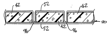
The gasket shown in FIGURE 1 has three seal seEl,l~nls 40, two outer se~ ; and acenter se~..~ , each of which is elongated and ~q.~j~a~Pnt at least one other ~ It would
also be pos~il,le to provide scgllle,nl~ in other shapes, for e~ le being laterally elongated
rather than longih--linAlly or made in other shapes that can reside alongside one a~lll.,. . Each
seg.. ~ 40 has a resilient core 42 which in this embodiment is generally 1~ gll1Ar in cross
section. The llul"~l of segmPnt~ can be varied, it being ~l~ fe"~d to use as many se~ f~ as
needed to cover the required area, each segmPnt being of a width limited to an easily produced
width chara~;s .i~lic of linear seals, for example about 1-3 inches (2.5-7.5 cm) in width.
The seal segmpnt~ 40, and gasket 20 as a whole, need only be ~!~rr.~ y thick to
30 e~co,~ ass the e~llc~ variations in the width of the gap ~n the sealed co..~ c~ , bodies
30, 32. Gasket 20 is held with some co, ~ ;.sion bel~cen bodies 30, 32, and is s~ ntly
21 76638
,
resilient to CollÇo~ closely to both conductive bodies. Where a~ploplidle, for example to seal
against a surface other than a flat surface such as along a ridge or groove, individual segm
can have a dirr~le,~ size, shape, width or ~ L IIPS~ than the a~l3~rPnt seg...~..l(s). It may also
be a~plo~liatc to vary the ~ L ..Pss or width of se~ bclwcen flat conductive bodies, for
S example providing thicker se~npntc for higher colll~r~sjion and better ele~;llical contact in some
areas as owoscd to others, such as along the outer borders of a gasket.
Each seg...~ 40 has first and second contact sl~rfac~s for bearing against bodies 30, 32
on opposile sides of gasket 20. Se~ 20 likewise have o~osile el~ng:At~Pd edge s~rfAtes 46,
which abut one another in the embodiment of FIGURE 1, and end ~ulLces 48. In this
10 embo-limPnt the resilient core 42 is ~b~ l;AIly ~ullouuded by an el~ AIIY co~ uc~ivc
material 52 which pl~Ç~,.ably covers at least contact surfaces 44 and edge surfaces 46. Insofar
as the gasket is cut through, for example along end surfaces 48 and ~ l~r~l~s along one or more
outer edge ~ulraces 46, resilient core 42 is c~l.ose~l.
The resilient core 42 can be con~ ctive or llollcolhluctive and can be a rubber or a
15 polymer, provided the core is u~rr~ ly resilient to press the cou~lu~;live co~ g ~ t~ ~ ;Al 52
into good electrical contact with the bodies 30, 32 to be sealed. Core 42 can be molded,
extruded, cut from a block, cured in place, etc. Preferably core 42 colupliSeS a polymer such
âS foamed polyul~ e or the like.
The f~ Ally conductive mqt~riAl 52 can C~ Jli~ various forms of woven or non-
20 woven co~lucLivc mqt~riAl snffi~i~ntly flexible to courollu to the collt{ ul of co~lu~ [;v~; bodies30, 32. For example, metal foil, screen, wire mesh, braided, woven or knitted wire or
m.-tqli7~ fibers, and the like, rnade from or iuCOI~Glatillg metal sheet, fibers or particles, can
provide a sllffri~ntly flexible and electrically con~ ve surface. Preferably, covelillg material
52 Collll)lises a fabric or thin batt il~col~olating metal fibers, metal alloy fibers or m~t~lli7~d
25 synthetic fibers. Al~ ivt:ly or in addition, a conductive coating can be provided in the form
of a cured polymer incorporating a ~sl~e~l~ion of collllu.;Live particles, such as a colloidal
~n~ion of cO~ ctive carbon particles, e.g., carbon black or spe~if~ ly acetylene black.
In a p~fell~d embo~lim~nt, the c~ ;ng m~teri~l 52 colll~lises a woven or non-woven fabric
of m.otzlli7~d nylon (polyamide) fibers. In a non-woven fabric, the fibers or fil~mf~nt~ can be
30 ~unbo~ded or rh~ ir~lly bonded or heat bonded to --zi-.~ illt~ , and either m.o.tzlli7l~d
by a plating ~rhn,~ e or originally formed to include metal particles, fibers or fil~ . In
- 21 76638
-
a woven fabric, Monsanto "Flectron" nickel/copper m~tAIli7~A polyester fabric or the like can
be used as the conductive surface material 52. The ~lhllaly functions of the surface nldl,ial
are to provide a conductive surface for ~ng~gin~ ele~tricAlly with bodies 30, 32, and an
cl~-ll ;cal connection belweell o~posi~ faces or sides 44 of se~.llf ~ 40.
S Seglll~ 40 are placed ~dj~eent to one a~ cr in a coplanar configuration, preferably
al,~lll;l~p along their ~ .,. edges 46, and are coupled together l~.~hq-~irqlly and electrically.
In the embo~im~nt shown in FIGURE 1, se~- ,.lc 40 are coupled in a hinge like fashion using
lengths of flexible conductive tape 54, preferably applied along lon~ih~dinql seams 62. The
con~ rtive tape 54 can col~lise a mqtçri~1 similar to that of su*ace covering 52, for e"~l;le,
adhered over at least a portion of the width of the a~'j7~ent se~ n~ at each seam by a
conductive adhesive or by a heat bol~ding t~rhni~ e such that the surface of gasket 20 bea.ing
the colll1uclivt: tape is s~b~l~--l;Ally evenly smooth for good conro~ y with the ~ ~live
co~ ive body 30, 32.
Conductive tape 54 can be applied to both opposi~ contact ~lllra~e-c 44, but theembo~1imrnt of FIGURE 1 has the seE,~ joined together by conductive tape appliedexclusively to one of the opposite contact sllrfarsc 44. An advantage of applying contluctive
tape 54 to one contact surface of the adj~xnt seE...~ 40 (as opposed to both) is that the two
a~ crnt se~"~ 40 can hinge or fold freely be~w~en the coplanar position, as shown in
FIGURE 1, through a 180 range of motion until the contact s~. r~res of the two ^~j~rPnt
se~.. - -.l~ contact each other, to stack Se~;JI'f~ ; 40. Of course the gasket can also .~o..
odate
curves, bends or angles to any point within the range.
It is app,~,ciated that a variety of co...l.~-liv~ tape and s~g.~ n configl~rations are
possible. A seal can be formed with m~ltiple se~ s wh.,r~ one or more ~ fxnt se~y.~*~
are joined by col~luclivc; tape applied to a first of the opposile contact surfaces and one or more
25 ;Idj ^çnt seE~"~e"~ are joined by col1lucliv~ tape applied to the opposite contact slrf~r~,
the direction in which the se~ can be bent or folded.
ively, the conductive tape can be applied to the first contact surface of one
jac~nt se~ --l and the opposite contact surface of the next ~dj~cPnt seg-~ pC~ g two
~djae~-~l s~...~ to hinge or pivot in either direction. Such an a"~gemell~ is not plf fe.,~
30 if the conductive tape is not ~tt~ rd along the edge surface 46 of at least one of the a~ rPnt
seg...~ , so that the segmrnt~ cannot be pulled laterally away from one another, leaving a gap.
21 7~638
For those applications requiring m~imnm seal ~ and rigidity, as opposed to flexibility,
conductive tape can be applied to both opposi~e sides of the two ~ijacent æg...~Additionally, those edge surfaces that have been cut through and where as shown in FIGURE
1 the core 42 is not covered with the conductive material, can be wl~ped in c~ hlctive tape
S to further ~ a~ te the resilient core and to provide additional coll.lu~live material bridging
bcl~n the sealed co,.~ ;ve bodies.
FIGURE 2 is a plan view of an exe~ l~y embodiment of the gasket 20, from the
bottom in FIGURE 1, namely on the side o~l,o~ile from the co~ ctive tape 54. This gasket
is suitable, for example, to æal bc.~l~ a c~ ivt; h~usi~g and the end flanges of circuit
10 cards, for e~ le metal ~ ded plates con~ ;n~-~lly ~ hfA to certain types of circuit
cards and in~h~ com~ec~l~ for signal or power lines to traverse a ~hi~lfling barrier. The
gasket can be used, for example, in a coll~u~. chassis for this ~ ose, and in that application
can be, for e~l~lc, a~r~ ldt._l~ 30 cm long, 13 cm wide and 0.3 cm thick. The spe~;irlc
~l;,.,f ~io-.~ of the seal of course can be varied over a wide range of sizes, shapes and/or
15 cf)~ ";on~ of sizes and/or shapes, to suit the application.
Rei~lling to FIGURE 2, in this embo~ n~ the seal is formed with a plurality of
cle~ilce opening~ 64 which traverse the two o~o~i~ contact surfaces 44 and a portion of the
resilient core 42 at each o~l,lllg 64. The o~mll~ preferably are die cut after contiml~us
seg....~ 40 have been ~ A toEether to form a ~rl~rie~l width, the die cuts fo~ ng the
20 pattern of openi~gs needed for a particular device, and ~t~ ially also cutting through one or
both of the çnAmost se~...P-.Ic to provide a gasket width that is less than an integer multiple of
the se2;.-.~ width. The o~ and the gasket width can also be forrned by other m~thoA~s
involving cutting or the assembly of short seg...~..l lengths so as to define the required cleal~ce
opel~ill~ 64.
The width of the O~l~illgS as shown can exceed the width of one or more s~ .lc 40
~l~ll the en~lmost seg..~ , which makes that se~...P .I (the center segmrnt in FIGURE 2)
discontimlol-s along its length. Nevelllleless, the gasket 20 PYt~nAc continl~o~cly around the
of each cleal~nce O~illg where, p~f~lably, at least a portion of the gasket is
colll~ressed bel~l facing surfaces of bodies 30, 32.
Adhesive strips 72 preferably are applied to at least one of the opposite contact sllrf;~ces
44 as shown in FIGURES 1 and 2, and can have pull-off film co~v.,ling the adhesive until the
21 76638
-
gasket 20 is ready to install on a conductive surface of bodies 30 or 32. Al~.~ivcly, other
forms of f~le~)~.s can be provided, such as holes to receive screws or rivets or the like.
The seal is particularly suitable for chi~ldin~ within the chassis of an elccllol~ic device
such as a digital CO~ ut~ ~, co~ ;r~tions a~alalus or the like having a plane of co..~rlu-
~
5 or similar t~ ions that need to traverse the shield barrier, usually via shiPl~ l co~ o-~.
FIGURE 3 shows how the invention can be applied to a typical ~l~onal co.~ t ~ chassis 80
having a backplane 82 fonned with a plurality of Opcl lllgS which col.e;,pond one for one with
a plurality of COI~ Ol sockets (not sho vn) on the co~ t L motherboard 84 m~ ntPA on the
bottom 86 of chassis 80 for ~;vi~g circuit cards 88. This type of ch~cci.c, m~tLc;,l~ald and
10 circuit card configuration is well known for PC cn...~ on~l COl~ , pl~,iding a
series of circuit card positions that are initially closed by cover plates (not shown) and can be
populated with any of various types of circuit cards 88, frequently having end flanges 30 that
usually have con~;~ol~. The chassis and backplane are ~ ded and form a part of the
.chi~l.li~ barrier. The gasket of the invention is advantageously placed over the backplane and
15 co..~ Ps the co~.hl~;Li.~e seal barrier across any gaps bcl~.l the backplane and the circuit card
end flanges 30 (or ~lcfl~ the cover plates for empty circuit card positions3.
Gasket 20 ovell&ps both the inner surface of the backplane and the rear facing surface
of the circuit card flange or other col..~ ive body 30 disposed inside of the shield barrier. The
gasket 20 is preferably 9~r.hed to ba~L~ - 82 via adhesives or f~rJ~f.~ or the like, the
20 ~ulllbel, shape and position of the openillgs 64 in the gasket COll~ ;,pol~dillg to t_e ,....,.h.f,l, shape
and position of the ~el~illgs in the b~cLrplqn~ elul..;..~ briefly to FIGURE 1, the seal is
sandwiched ~n flange 30 and ba~l~plqnP 32 (or 82 in FIGURE 3), the seal providing a
resilient sealing surface bclweell the flange and the backplane. In operation the seal is
col~l~;,sed, as shown in FIGURE 4, to provide m~ximl-m electrir~l colllilluily be~,ell the seal
25 and the flange or the seal and the bac~lalle in the particular application.
The el~octric~l Cil-;Ui~ ' on the motherboard and/or printed circuit cards ge~ t~s ~ ing
levels of EMI. The EMI which is in~ lent on gasket 20 is reflected or lics;l~ in the form
of Cu~ in~ ling co~ l;on through gasket 20 to ground. Gasket 20 accol~ lg to theinvention a~eal~ to be less contimloll~ than a comparable gasket having a single integral core
30 of the full gasket width and a colhl~ iv~ surface çx~ contimlollely around the core.
However, the invention is in fact c~.n--t~ ed by shorter colllu~;liv~ paths and ll.ll~,fol~ lower
21 76638
electrical l~ ci~ re bclwcen any two given points, for example on opposite sides of the gasket.
Thelcfolc, the invention has better ~hi.olrling efficiency than a continuously wrapped single core
of the same size and elccLIu~ n~tir chalact~ ics.
This can be applccialcd with çcf,_lel~ce to FIGURE 4. A pot~ ial relative to ground
S in~1uced at a given point 92 on the conductive co., hlg 52 on the first contact surface 30 (e.g.,
facing the mulh,_lboard and printed circuit cards in FIGURE 3) induces a current that is c~llpled
to ground (~ mf d to be the chassis backplane 32 or 82) along a path (shown in a heavy broken
line) through the conductive material of covering 52 to the opposi~c contact surface 44, which
bears against the backplane. FIGURE 4 is a detail view showing portions of two ~djac~
10 se~f~ of the seal affixed bcl~ l the col~-lu~livc bodies, the yot~lltial being A~ ed to be
in-hlc~ on the top surface in FIGURE 4 to be sinked at a ground coupled to the bottom surface.
ShirlAing effir,;f~nr,y COIll~)alCCl to non seE ~ -.t~ co~ ulalion is hl~ylu~ed beca~se the
segm~ontf~l ~ ule of the seal provides shorter conductive paths for eddy ~;ull~,nls, as shown
by dotted line arrow 90. This path goes along the edge surface 46 of the subject Sf ~
Actually, the path for the current inrludes all the paths that couple bc~.,el1 the point 92
of the ~olen~ial and ground. These paths crrc~;livcly form parallel electrical ~ r~s that
cQmm~ ly define the l~,s;~ e bcl~ce~ the t~-vo rcfel~ .lce points at the in~ c~ yo~ll~ and
at ground. Whereas the h~ LiOll provides shorter and more llulll.r~us paths than a
COntinllOll~ly Wlap~d all~.-g.--..~ in which the paths n~s~l ;ly pass around the e~ l,lc edges
20 of the gasket, the l~,s;x~ e is less and the ~hi~l~ing crÇcclivcl~S5 of the invention~is greater
t~n in the contin~ cly wla~ped gasket.
FIGURE 5 illll~ rs an ~lt*rn~tive embo~im~r~t wll~ hl the sez~ d gasket is cut not
only at a clearance opelli~ 64, but also along one edge 94, at which the conductive co~,lhlg
52 has been cut away for providing the desired width of the gasket 20. Accoldi~ to this
25 emb~imPnt, a potential a~ljacel-t the cut edge l~p~se.lt~ a worst case condition wll. lchl the path
to the o~osilc side passes around the edge surface 46 of the ~csoci~tç~ seg,--~-.l This path is
longer than if the edge is not cut, but due to se~s~.,r~ ion according to the invention, the worst
case path is still, at most, a fraction of the chculllfel~llce of a single seg~ . FIGURE 5 also
illu~llales an embo~im~nt wherein the conductive tape joining ~dj~ent segments has been
30 replaoed by a conductive adhesive that holds the edges 46 of a~jaoent sæg~ in al,~
21 76638
In a pJcfe,l d embodirnent, col~JucLivc tape 54 can be the same type of material as the
conductive covering 52, such as a conductive m~t~lli7f~1 fabric. A foil, conductive polymer
layer or similar structure providing a coll~lu~liv~ material bridging over the seam is also
possible, these being exemplified generally by conductive tape. The conductive tape 54
5 preferably is affixed to covering 52 using a conductive adhesive. The conductive adhesive has
a volume conductivity and joins the coll-luelivc tape 54 to the col~-lu~liv-e covering 52 relatively
fully over the area of overlap. It is also possible to employ a nonconductive adhesive where
the area and/or intim~ry of co~Llucliv-e contact belweell tape 54 and covering 52 provides the
CesC~ electrical connection.
A pl~f~ d all; I-ge~.. f .. l of the Sf~J~ iS shown in FIGURE 6. In this embofiimf nt,
co~lu~;live tape 54 joins over a~j~cel t seg...~ and holds their edges 46 against one another.
The tape 54 is provided only on one side, and on the o~posile side thin adhesive strips 72 are
provided (see also FIGURES 1 and 2). The adhesive strips can be provided in whale~e.
ge~ n that is conven~ l for holding the gasket in place, at least lelllpol~lily until it is
15 affixed by e~m~ont l~l-. ~n conductive bodies 30, 32. Of course other means for ~tt~rhin~
the gasket to the bodies such as f~c~n~rs, colll~ mPnt~ry contours for receiving the gasket and
the like, can be employed instead of or in nd~ition to adhesive strips 72.
In addition to the dirr~ choices of materials and sll.l~;~al allange,llents lic~
above, the invention is subject to other variations which are app~ ~l in view of the fol. gOillg
20 eA~lcs. For eY~mple, the invention is disclosed in the form of a relatively thin and flat
gasket suitable for sealing bel~ flat conducdve m~mhers. The seg...f ~ l;on also allows the
gasket to smoothly seal curves, at least on one axis of ~;ul~dtule parallel to the seams ~lwc~ll
se~...- .1~. A two ~ ion~l array of segllR,I~ could be employed to seal around a curve in
two axes, or a more complex shape. The invention could also be configured such that edges
46 having a greater 3im~ion than the width of contact faces 44, or these two ~ iions could
be equal in a gasket where the Sc~ f~ are s~l,s~ lly square in cross section.
Likewise, not all the segmfnt~ need to be the same size or shape. For example, the
se~ s in certain areas can be thicker than in other areas so that the colll~lession is greater
at the thicker segments. Nor must all the segllle,l~ be con.l~clivt;. It is possible in certain
30 applir~ion~ to employ llollco~luctive se~~ , for example, in one or more int~rrn~i~te
segm~ntc, with conductive segm~ntc at the edges.
21 76638
14
Other variations are also possible. For example, the segments that are ~tt~ch~ and
electrically coupled need not be fully formed elongated EMI seals, but can co,~ ise merely
collll)r~sjible cores that are then ~tt~rh~d in a manner providing conductive surfaces and
ele~;llical coupling l~el~. ell the opposite surfaces b. ~.~n the seals. Examples are shown in
S FIGURES 7-10. In FIGURE 7, co~lueli~e surface material 52 is joined electrically across
opl)osile faces of the gasket along depressed seams 96. In this example, material 52 co~ ,ises
continllol-~ sheets disposed on each side of the gasket. On one side (the bottom as shown), the
sheet material is flat, and on the other side is diverted in a narrow U-shape ~e~ l each core
segm~nt 42. At the bottom of the U-shape, material 52 is electri( ~ y coupled, for example by
10 colnl~ e adhesive, or more pl~f._.dbly, by- heat sealing material 52 along the seam ~urr~ciel,lly
to bring the co~ cli./e fibers or the like of material 52 into contact. This forms a gasket
providing the same ~hiPl~1ing advantages as the ~l~ gOillg embodi.~ s, and is relatively easy
to produce.
FIGURE 8 ill~llales a further embodirnent similar to FIGURE 7, in which the d~less~l
15 seam lines 96 are provided in an ~ manner on o~posile sides of gasket 20. FIGURE
9a shows an embo-lim~nt wherein the seam lines 96 are formed by U-shaped depressions on
both sides of the gasket; however, the depression on each side e~rt~nrls only part way through
the ll~i~L..fs5, e.g., half way. This allows gasket 20 to bend freely in either direction. As in
FIGURES 7 and 8, Illat~.ial 52 can be heat sealed to achieve ele~l.ical coupling, or coupled
20 using colldu~ re adhesive.
In FIGURE 9b, an ~ll....~ti~e is shown wh. ~ the se~ lap on al~ll~l and is thus
similar to FIGURE 9a except that the outer facing surfaces of the gasket are more continuous
(i.e, the seam gaps are small).
the embo~lim~ont~ of FIGURES 7-9b employ conductive a&esive, the adhesive
25 is thin. In FIGURE 9c, a structure similar to FIGURE 9a is provided, but the O~OSilè portions
of sheet material 52 are joined by conductive ~ i"~. The ~ hi"g can be, for examplê, a
zigzag stitch as shown, with each pass through mqt~oriql 52 located imm~o~iqtely ~q~dj~cent a
se~ core 42. The stitt~in~ also can be passed directly through the core.
By using a thick bead 97 of conductive adhesive as shown in FIGURE 10, conductive
30 mqt~riql 52 can be flat and contin-lollc on both sides of gasket 20. The colhlu~live adhesive is
provided belween adj~cent core seglll.,lll~ 42, that are wlil~ped commonly with con~1uctive sheet
2 ~ 76638
m~tPri~l 52. This provides electrical connection be~w~en opposite sl~rf~ces of gasket 20 in a
manner similar to seams 96, provides a relatively smooth and continuous surface on both sides,
and securely ~tt~rh~s the a~ ont core segm~nt~ 42.
In the embo(1im~ont~ of FIGURES 7-9a and 9c, the U-shaped depl~ssions fo~ g searns
S 96 p.efelably are kept narrow. Th,l~,fol~" when gasket 20 is CCm~ ,SSed be~ op~osed
conductive bodies, col~ .,s~ion of core segents 42 tends to bulge the se~ laterally and
into contact with one alwLll~r, closing the U-shape laterally. Provided searns 96 are suitably
narrow, these embo~ thus also provide ~lb~ ly contin~lous surface contact with the
conductive bodies. The particular width of the U-shapes needed to achieve ~!.rr~ri~ ~l bulging
10 to obtain contact will vary with the coll,~l.,;,sion ch-. ~et isLics and the extent of col~ ,sion
of the core seg,..~ 42.
FIGURE 11 illustrates a slightly dir~ embolim~nt ~1R~111 seams 96 are formed
using a linear conductive material 98 that pierces through the o~posi~ layers of co~ cl;ve
material 52. This linear conductive material can be continuous, in the lllanl~ of s~ with
wire or con~lucLive thread or yarn, or discontinuous, in the ll~llRr of staples or p~ l.~s an
upholstery button tuft stitch.
FIGURES 12a through 12f illustrate a series of teehni~les for dealing with the
co~ Liv~ sheet material along an edge of the gasket, for e~ le along a lon~itl~lin~l or
lateral edge. These techniql)es can be used to cover over the foam core at an edge, either
originally or after die cutting. In FIGURE 12a, co~ n;~;ve material 52 is de~l~,3sed from one
side, similar to the seam of FIGURE 7, and in FIGURE 12b material 52 is deplessed
symm~tlir~lly on both sides as in the seam of FIGURE 8. In either case the ,~ l 52 on
opposite sides of gasket 20 is brought into electrical contact. The l~lgillS of material 52 along
the edges can extend beyond the edge of the coll~s~ol1dillg core seg...~.l 42 such that they can
25 be heat sealed together or att ~hrd with conductive adhesive. In the event of a die cut that
removes any material 52 ~ .li"g beyond core 42, heat sealing can be used in part to melt a
portion of core 42 such that the edges of material 52 can be brought together and heat sealed
m~nn~elves.
In FIGURES 12c and 12d, edges ç,~..,.l;"~ beyond the edge of core 42 are Wl~)ed
30 around the edge and overlapped, preferably being also heat sealed or coupled using conductive
adhesive. The overlap can occur along the edge (FIGURE 12c) or on one of the faces of gasket
2 1 7663~
16
20 (FIGURE 12d). As shown in FIGURE 12e, it may not be ..~c~. y to overlap the edges
of conductive sheet 52 along an edge to achieve a cGl~-lu~;live path bel~n the opposite faces
of gasket 20, around the edge. In FIGITRE 12e, the sheet 52 on one side (the top as shown)
eYt.onfls around the edge and resides along the margin of the oppo~ile edge for mqking e~ectrirq-l
5 contact with the COll~ s~ol~dillg co~lu ;Li~re body. ~f~,ldbly, ho~ e., any gap bct~n the
extreme edges of the conductive material 52 is minimql, e.g., 0.02 inch (0.5 mm) or less, to
provide s-ll,s~ lly full contact be~en gasket 20 and the co..~ c~;~e bodies. FIGURE 12f
ill~ll~t~ s that the CGl~ lion of the t.. - ...;..~l edges 99 can also be made by a conductive thread,
staple or similar r~t~ , dS ~ ç~ above.
The invention having been ~ se~ in co~ on with the fol~,goillg vqriqti-~nc and
e~...ples, additional ~ iaLions will now be al,p~ lL to pe.~ns skilled in the art. The invention
is not int~m1ed to be limited to the variations specifically mentioned, and accoldil~gly lefe~ ce
should be made to the appcl~ded claims rather than the fol.,~in~ .JssiQn of pl~,f~
examples, to assess the scope of the invention in which exclusive rights are clq-im~.