Note: Descriptions are shown in the official language in which they were submitted.
2t ~6~
MULTI-PORT RANDOM ACOESS MEMORY
TECHNICAL FIELD
The present invention relates to a multi-port random access
memory.
BACKGROUND ART
Well known RAMs (random access memories) have at least one
address port and include storage elements (core cells). In a paper by A.L.
Silburt et al entitled "A 180-MHz 0.8-,um BiCMOS Modular Memory Family
of DRAM and Multiport SRAM", IEEE Joumal of Solid-State Circuits, Vol. 28,
No. 3, March 19g3, p. 222, at 227 and 228 show various RAM core cells.
It is a problem to develop a practical, high-speed, low-power and
area efficient core cell to support multiple ports (e.g., a single high-speed write
port and four high-speed read ports). A conventional five port cell would
have required ~ irn~1 access lines and ci~nihrAnt area to achieve adequate
2 0 stability margins.
In a FaPer by G. Gerosa et al entitled "A 2.2 W, 80 MHz
Superscalar RISC Microprocessor", IEEE Joumal of Solid-State Circuits, Vol.,
29, ~o. 12, December 1994, p. 1440, at 1447 shows a RAM storage element with
2 5 single-ended write access structure. The disclosed structure of five ports (one
write port and four read ports) indudes a plurality of transistor stacks whidh
are cr,nn~rtP ~ to ~ e~tiv~ bit lines. Each transistor stadk has top and bottom
MOSFETs (metal oxide s~ tor field effect l. ,~ lo. ~). The drain-
source circuits of the top and bottom MOSFETs are series-conn~r~P~ The
3 0 gates of the bottom MOSFETs are connected to ~e.L ~ ~ read port lines. The
gates of all top MOSFETs are in parallel connected to the core cell. This
results in llnnrr~cc~ry loading on the bit line, since the full MOSFET channel
capacitance and internal diffusion r~r~ri~n~ of the top MOSFET in the stack
is added to the bit line load for every core cell storing data which will set the
3 5 gate of the top MOSFET "high". This may as mudh as double the bit line load,
2~ ~66~5
resulting in ci~,,.;r;. ,,,.~ly reduced ~1~, r,., ...~".~,~ Furthermore, the
imrlPm~nt~tion described in the paper uses only single-ended read access
which, for all but the smallest mPmori~C, may result in 5~lhstantl~lly inferior
read p~, ~.,....~". ~
United States Patent No. 5,404,455 granted to D.F. Daly et al on
April 4,1995 discloses a TDM (time division mllltirl~Y~r) scheme for
~Itl~rn~tin~ mmllni-~tinn between a pair of RAMs. In a paper by C. Ohno
en*tled "Self-Timed RAM: STRAM", FtJJlTSU Sci. Tech. J., 24, 4, December
l 0 1988, p. 293 shows a self-*med RAM which has synchronous operation and
an on-chip write pulse generator.
The problem is to develop a practical, high-speed, low-power
and area efficient read port structure to allow multiple (e.g., eight) random
15 access reads per clock cycle. The straight forward ul.~1~,,,. ..1.3*rn of multiple
physical ports throughout the memory would be prohibitively complex and
in~ffl~i~nt.
In a paper by F.E. Barber et al, "A 2K x 9 Dual Port Memory",
2 0 ISSCC Dig. Tech. Papers, Feb. 1985, pp. 44~5 and in a paper by F.E. Barber et al,
"A 200ns 512xl0 DUAT. PORT RAM", Proc. Electron. Con, vol. 36, Oct. 1982,
pp. 380-382 disclose a single port RAM with two a~yl..luu~.uLls address, data
and control intPr~rl~C Timing is controlled by arbitration between address
latch enable signals. A memory access from port A is initiated by asserting the
2 5 address latch enable signal "low" on port A, an access from port B is ini*ated
by asserting the address latch enable signal "low" on port B. If port B attemptsto access the memory while port A is actively accessing the memory, then an
arbitration circuit will delay the port B access until the port A access is
complete. In the RAM, .I:lyl~ lu~lou~ enables are used to initiate memory
3 0 access.
In a paper by T. ~tCllmllra et al, "Pipelined, Time-Sharing
Access Technique for a Highly Tnt~gr~h~l Multi-Port Memory", Symp. VLSI
Circuits Dig. Tech. Papers, June 1990, pp. 107-108 and in a paper by K Endo et
3 5 al, "Pipelined, Time-Sharing Access Technique for an Integrated Multiport
21 76675
.
Memory", IEEE J. Solid-State Circuits, vol. 26, no. 4, pp. 549-554, April 1991
disclose a dual port memory with respect to a common clock (CLK) which is
controlled by common write enable (WE) and chip select (CS) inputs.
Likewise, ports 2 and 3 are ~yl~LlllulLo~ with respect to a common clock and
5 control inputs. All inputs for ports 0 / 1 are latched on the rising CLK edge of
the port 0 / I dock input. All inputs for ports 2 / 3 are latched on the rising
CLK edge of the port 2 / 3 dock mput. Port pairs 0 / 1 and 2 / 3 are time-
ml1lhrlrY~d by their respective clock inputs. Port 0 access is active when the
CLK input for ports 0 / 1 is high, port 1 is active when the same clock input is10 low. Likewise, port 2 is active when the CLK input for ports 2 / 3 is high and
port 3 is active when the same clock input is low. Output data is then re-
timed in a pipeline cycle and is presented to the outputs relative to the
e.Llv,~ rising dock edge. Described is a synchronous time-shared access
technique that is dependent on the clock duty cycle (duration of the clock high
15 period and clock low period) with half of the memory aesses occurring
while the clock is high and the other half occurring while the clock is low.
SUMMARY OF THE INVENTION
2 0 It is an object of the present invention to provide an improved
multi-port RAM (random access memory).
In accordance with one aspect of the present invention, there is
provided a multi-port RAM having an array of RAM cells, each RAM cell
2 5 comprising: at least one pseudo-dirr,-"-~.lial write access port; at least one
dirrt~ .lial indirect read access port; and a storage element having first and
second data input/output terminals, the storage element p~ r~ a data
latch function for storing binary data.
3 0 In one example of the multi-port RAM, a pseudo-.lirr~l~l,Lidl
write access is provided by ~:ul~dllc~iv~-nnnrnnr~l~c~ive means. During a
"write" operation mode, the conductive-nn~ ;v,~ means provides a
binary data signal to either of the terminals of the core cell, in response to awrite word line signal. The data signal ~:ull~-~uo~ds to "zero" or "one"
3 5 derived from a write bit line. For example, the conductive-nonronrlllr~ive
~ 5
means includes FETs (field effect ll~llcic~ ) The drain-source of one of the
FETs is rnnnrrh~CI to the terminal of the wre cell and a write bit line on whichthe binary data signal is present. The drain-source of another FET is
rnnnr-rtl~cl to the other terminal of the core cell and an indirect bit write access
5 FET. The binary data is written into the wre cell via the conductive FET and
latched therein.
In another example of the multi-port RAM, the core cell is
rr)nnrrteCl to a plurality of read word lines and a plurality of pairs of read bit
10 lines. During a "read" operation mode, dirr~ al data is present on a pair of
bit lines. The dirrelel.Lidl indirect read access is provided by a pair of gating
means for one pair of bit lines, each gating means being rnnnr-rt~cl between
each of the terminals of the core cell and one of the differential read bit lines.
For example, the gating means includes FETs which are controlled by read
15 word line signals. While a read word line is acHve ~i.e., the "read" operation
mode), the FET (of the gaHng means) to which the read word line corresponds
transfers the data latched in the core cell in a differenHal form to the pair ofbit lines.
2 0 In a~wldc~Ll~e with another aspect of the present invention,
there is provided a multi-port RAM having an array of RAM cells, each RAM
cell comprising: a storage element having first and second data input/output
terminals, the storage element pel~ullllillg a data latch function for storing
binary data; conducHve-nnnrnn~lllrHve means for providing, during a write
2 5 operation mode, a binary data signal to either of the first and second datainput/output terminals, in response to a write word line signal, the data
signal corresponding to zero or one derived from a write bit line; and a
plurality of pairs of gaHng means, each being connected between the
le~e~live data input/output terminals and a le~lue~live one of a plurality of
3 0 dirrelelllidl read bit lines. In the multi-port RAM, dirrelel.lial data is present
on a pair of read bit lines during a read operation mode in response to a word
line read signal.
In accordance with another aspect of the present invention,
3 5 there is provided a multi-por~ RAM comprising: store means for storing data,
2 ~ 75~7~
.
the store means induding an array of m rows by n columns of RAM cells,
with N read ports; and addressing means for g~nl~rAtin~ M address signals of
X- and Y-addresses in response to an input clock signal and an input address
signal of address inform~ti~n, the M address signals being generated during
5 one clock cycle of the input clock signal and being diferent in phase from
each other, the X- and Y-addresses of each of the M address signals idenfffying
the row and column of the array of the RAM cell, l~e.livt:ly.
In an example of the mulff-port RAM, the addressing means
10 comprises clock generating means for gl~n~r~tin~ first and second control
clock signals in response to the input clock signal. It further romrrig~c
address generating means for ~t:lLt~ illg the address signals of the X- and Y-
addresses in response to the first and second control clock signals,
l~a~e~LivL-ly.
In another example of the mulff-port RAM, the self-timed, time
multiplexed read port control is ill,~ d in a four physical port
structure. It allows the eight read ports to be imrlf~mPnt~d as four physical
port structures accessed twice per clock cycle. The number of the accesses per
2 0 clock cycle is two, for instance. No special control or clocking is requiredexternally to the RAM cell, since all timing is internally generated from a
smgle rising clock transiffon. The core cell may be a dynamic random access
memory cell or a staffc random access memory cell.
2 5 BRIEF DESCl~IPTION OF THE DRAWINGS
An embodiment of the present invenffon will now be described
by way of example with reference to the ~ ..yiLlg drawings in which:
Figure 1 shows the structure of Figures lA - lD which illustrate a
3 0 mulff-port RAM (random access memory) according to an ~mhofliml~nt of the
present invenffon;
Figure lA is a block diagram of an X-address circuit and a row
decode circuit which are included in the mulff-port RAM;
Figure lB is a block diagram of a mulff-port core ceU array which
3 5 is included in the mulff-port RAM;
21 76~7~
.
Figure lC is a block diagram of a Y-address circuit, a column
decode circuit and a clock generator which are included in the multi-port
RAM;
Figure lD is a block diagram of a bit line access circuit and a data
5 output circuit which are included in the multi-port RAM;
Figure 2 is a detailed circuit diagram of a RAM cell included in
the multi-port core cell array shown in Figure IB;
Figure 3 is a detailed diagram of a latch included in the RAM cell
shown in Figure 2;
l 0 Figure 4 is a detailed block diagram of the clock generator shown
in Figure IC;
Figure 5 is a detailed circuit diagram of the reset generators
shown in Figure 4;
Figure 6 is a timing chart which illustrates the operation of the
l 5 RAM cell shown in Figure 2; and
Figure 7 is a timing chart which illustrates the operation of the
multi-port RAM.
DETAILED DE~CRIE~ION
I. Entire Structure of an l~nnho~imPnt RAM
The entire structure of a multi-port RAM (random access
memory) of an embodiment according to the present invention will now be
2 5 desibed.
Referring to Figures IA - lD, a multi-port RAM has a core cell
array 110 of m (=48) rows by n (=64) columns with one write port and four
read ports. The core cell array 110 is connected to word lines 112 and bit lines3 0 114. Control circuits for the write port are not shown. Each RAM cell of thecore cell array 110 has a dynamic or static storage element. The word lines 112
are ~nnnPctPd to the row decode circuit 116. The address identifying the core
cell for data reading in the core cell array 110 is ~iPtPrminpd by X- and Y-
address signals which are provided by a row decode circuit 116 and a column
3 5 decode circuit 118, ~ liv~ly.
21 7~67~
.
The row decode circuit 116 has 192 row decoders (4 ports per row,
48 rows). The bit lines 114 are connected to a bit line access circuit 120 whidhhas 256 column access circuits (4 ports per column, 64 columns; 8 columns per
5 bit, 4 data buses per bit). The address data is contained in an address signalwhich is present on an address input bus 122, the address signal having X-
and Y-address data. The address input bus 122 is an 8 port x 9-bit address
input bus. The 8 ports are ~ led by "a" - "h". The Y-address data is fed
to a Y-address circuit 124 via an 8 port (ports a - h) x 3 bit (bits 0 - 2) bus. The X-
l 0 address data is fed to an X-address circuit 126 via an 8 port (ports a - h) x 6 bit
(bits 3 - 8) bus.
The Y-address circuit 124 has 24 Y-address registers (3 Y-address
inputs per port, 8 ports). The X-address circuit 126 has 48 X-address register
l S and predecoders (8 ports, 6 X-address inputs per port; 2-to4 predecode per
port). The X-address circuit 126 is connected to the row decode circuit 116 via
a predecoded row address bus 128. The Y-address circuit 124 is r~nn~ t~ via a
column address bus 130 to the column decode circuit 118 whidh is ~nnnf~t(~d
to the bit line access circuit 120 via a decoded column address bus 132 having
2 0 decoded Y-address lines. The column decode circuit 118 has 32 column
decoders (8 per port pair, 4 port pairs (a/e, b/f, c/g, d/hk 3-to-8 decode per port
pair).
Timing of addressing is controlled by a dock generator 134 whidh
2 S is a self-timed, time multiplex control circuit. A clock input line 136 to which
a system dock signal dk is fed by a dock source (not shown) is rnnn~rtl~fl to the
clock generator 134. Also, a mode line 138 to which a self-timing override
mode signal stov is fed by a signal source (not shown) is ~onnPf~fl to the
dod~ generator 134. The dodk generator 134 generates dodk signals of two
3 0 phases 01 and 02 and doubles the frequency of the dock signal by
ml1ltipl~ ~ Multiplex conkol clock signals crxl and crx2 rom the clock
generator 134 are fed to the row decode circuit 116 via multiplex dodk lines
140 and 142, l~e.liv.cly. Interface dodk signals cril and cri2 from the clock
generator 134 are fed to both the Y-address circuit 124 and the X-address circuit
3 5 126 via interface dock lines 144 and 146, ~ ,e.~iv~ly. Multiplex conkol dock
2t7~
signals cryl and cry2 from the clock generator 134 are fed to the column
decode circuit 118 via multiplex clock lines 148 and 150, ~ e.liv~ly.
A 01 precharge dock signal crpl and a 02 predharge dock signal
S crp2 are provided by the dock generator 134 to the bit line access circuit 120
via precharge lines 152 and 154, ~e-Lv~ly. A 01 sense amp latch dodk
signal crll, a 02 sense amp latch dock signal crl2 and an output register dock
signal crq are provided by the dock generator 134 to a data output circuit 156
via a sense dock line 158, a sense clock line 160 and a register dock line 162,
~ Liv~ly. The data output circuit 156 has 64 sense ~mrlifiPrc (8 per output
port, 8 output ports,) and is connected to an 8 port x 8-bit data output bus. The
data buses 164 from the bit line access circuit 120 are connected to the data
output circuit 156.
II. Detailed Structure of Circuits of the RAM
The following description assumes, for simplicity and purely by
way of example, that FETs (field effect ll.l~,sis~,.,) referred to are MOSFETs
(metal oxide 5Pmi~ tor FETs) and a supply voltage +Vcc is +5.0 volts.
(i) Multi-Port RAM Cell Array
The multi-port RAM cell array shown in Figure IB will now be
dPe~rihP~i Each RAM cell of the multi-port RAM cell array consists of four
2 5 differential read ports with indirect data access via gated, bit line pull-down
L~.l.;,lsl.,., and one single-ended write-only port with local bit line inversion
to give pseudo-d;r~l~:..lial write access.
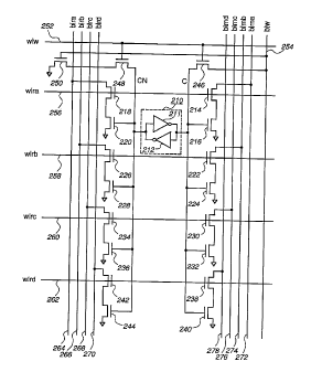
Each RAM cell of the multi-port RAM cell array has a five-port
3 O storage element (core cell) and includes one write port and four differential
read ports ~vith indirect data access. The RAM cell includes a latdh 210 which
has two mverters 211 and 212. Each of the inverters 211 and 212 has a CMOS
(connrlPmPnt~ry MOS) inverter. The input and the output terminals of the
inverter 211 are ~ ~nnP~`tP/1 to the output and the input terrninals of the
3 5 inverter 212, l~pe.Lv~ly.
2 1 76~75
The souroe of a FET 214 is connected to the drain of a FET 216
and the source of a FET 218 is connected to the drain of a FET 220. Similarly,
the source of a FET 222 is connected to the drain of a FET 224 and the source ofa FET 226 is connected to the drain of a FET 228. The source of a FET 230 is
rnnnP.-tP~ to the drain of a FliT 232 and the source of a FET 234 is l~rnnprtpcl to
the drain of a FET 236. The source of a FET 238 is connected to the drain of a
FET 240 and the source of a FET 242 is connected to the drain of a FET 244.
The output terminal of the inverter 211 and the input terminal
of the inverter 212 are connected to the gates of the FETs 216, 224, 232 and 240and the drain of a FET 246. The input terminal of the inverter 211 and the
output terminal of the inverter 212 are connected to the gates of the FETs 220,
228, 236 and 244 and the drain of a FET 248 whose source is ~ nnnprtpd to the
1 5 drain of a FET 250. The sources of the FETs 216, 220, 224, 228, 232, 236, 240, 244
and 250 are cr,nn~tP~1 to the ground terminal.
The gates of the FETs 246 and 248 are ~nnPctPd to a line 252 on
which a write word line signal wlw is present. The gate of the FET 250 and
2 0 the source of the FET 246 are connected to a line 254 on which a write bit line
signal blw ~ g data "zero" or "one" is present.
A line 256 on which a word line read signal wlra is present is
ronn~,-t~Pd to the gates of the FETs 214 and 218. A line 25g on which a word
2 5 line read signal wlrb is present is connected to the gates of the FETs 222 and
226. A line 260 on which a word line read signal wlrc is present is rnnn~rtPd
to the gates of the FETs 230 and 234. A line 262 on which a word line read
signal wlrd is present is connected to the gates of the FETs 238 and 242.
3 0 The drains of the FETs 218, 226, 234 and 242 are l r,nnP~tpd to bit
lines 264, 266, 268 and 270"~e~Liv~ly, on which read bit line signals blra,
blrb, blrc and blrd are present. The drains of the FETs 214, 222, 230 and 238 are
ronnP~ tpd to bit lines 272, 274, 276 and 278"~ e.liv~1y, on which read bit linesignals blrna, blrnb, blrnc and blrnd are present. The bit lines 264 and 272, 266
3 5 and 274, 268 and 276, 270 and 278 are pairs of bit lines and on the ,~e.Lv~
2~ 7~675
pairs, the read bit line signals blra and blrna, blrb and blrnb, blrc and blrnc, and
blrd and blrnd are which are differential signals are present.
Figure 3 shows a detail of the latch 210 of the multi-port RAM
S cell array. The latch 210 is a well known RAM storage element which
includes two CMOS inverters. In Figure 3, the drains of a P-channel FET 280
(a load device) and an N-channel FET 282 (a drive device), which define one
CMOS inverter, are connected to the gates of a P-channel FET 284 (a load
device) and an N-channel FET 286 (a drive device), which define the other
CMOS inverter. Similarly, the drains of the FETs 284 and 286 are ~ onnprt~cl to
the gates of the FETs 280 and 282. The sources of the FETs 280 and 284 are
rnnn~ t~i to the voltage terminal of the supply voltage +Vcc. The sources of
the FETs 282 and 286 are connected to the ground terminal. The junction of
the drains of the FETs 280 and 282 defines node CN. The junction of the
1 5 drains- of the FETs 284 and 286 defines node C Nodes CN and C are data
input and output terminals of the latch 210.
(ii) Clock Generator
2 0 Referring to Figure 4 which shows the clock generator 134 in
detail, it has a 02 timing generator 310, a 01 timing generator 312, a buffer 314,
a NAND gate 316 and a buffer 318. The clock input line 136 to which the
system clock signal ck is fed is connected to the 02 timing generator 310 and
the 01 timing generator 312 and to input terminals of the buffers 314 and 318.
2 5 The mode line 138 to which the self-timing override mode signal stov is fedis onn~ f~cl to the 02 timing generator 310 and the 01 timing generator 312.
The buffer 314 delays the system clock signal ck and provides the output
register clock signal crq on the register clock line 162. The buffer 318 delays
the system clock signal ck and provides a 01 read clock signal crl. The output
3 0 terminal of the buffer 318 is connected to the 01 timing generator 312 and the
NAND gate 316. The 02 timing generator 310 has two AND gates 320 and 322,
a 02 reset generator 324, two inverters 326 and 328 and a buffer 330.
The 01 timing generator 312 has two ~ND gates 332 and 334, a 01
3 5 reset generator 336, two inverters 338 and 340 and an AND gate 342. The clock
2 J ~75
input line 136 is .~r.nnl,rt~,l to the buffer 330 and the AND gate 342. The buffer
330 delays the system clock signal ck and provides the interface clock signal
cri2 on the interface clock ]ine 146. The output terminal of the buffer 318 is
l onn~rtP~I to the NAND gate 316, the AND gate 332, the AND gate 334 and the
S 01 reset generator 336. The output terminal of the NAND gate 316 is
rnnn~l t~d to the AND gates 320 and 322 and the 02 reset generator 324. The
output terminal of the AND gate 322 is connected to the 02 reset generator 324
and the inverters 326 and 328. The output terminal of the AND gate 334 is
~nn~rt~cl to the 01 reset generator 336 and the inverters 338 and 340.
1 0
The self-timing override mode signal stov is fed to the 01 and
the 02 reset ~ laLOI ~ 336 and 324. The override mode signal stov is a
nosti~ mode control input signal and it is "high" and "low" in hormal
and ~ n~lStir modes, ~ e.Liv~ly.
The 01 reset generator 336 provides a 01 reset control signal rstnl
on its output terrninal which is connected to the NAND gate 316 and the
AND gates 332, 334 and 342. The NAND gate 316 provides a 02 read clock
signal cr2 which is a NAND logic signal of the 01 read dock signal crl and the
2 O 01 reset control signal rstnl. The 02 reset generator 324 provides a 02 reset
control signal rstn2 on its output terminal which is ~nnPctf~d to the AND
gates 320 and 322. The AND gate 320 provides the multiplex control clock
signal crx2 on the multiplex clock line 142. The multiplex control clock signal
crx2 is an AND logic signal of the 02 read clock signal cr2 and the 02 reset
2 5 control signal rstn2. The AND gate 322 provides the multiplex control clocksignal cry2 on the multiplex clodk line 150. The multiplex control clock signal
cry2 is an AND logic signal of the 02 read clodk signal cr2 and the 02 reset
control signal rstn2. The inverter 326 provides the 02 sense amp latch clodk
signal crl2 on the sense dodk line 160. The 02 sense amp latdh dock signal
3 O crl2 is an inverted signal of the multiplex control clodk signal cry2 The
inverter 328 provides the 02 predharge dodk signal crp2 on the ~I~.IIal~,~ line
154. The 02 precharge dodk signal crp2 is an inverted signal of the multiplex
control clock signal cry2. The AND gate 332 provides the multiplex control
clock signal crxl on the multiplex clock line 140. The multiplex control clodk
3 5 signal crxl is an AND logic signal of the 01 read dodc signal crl and the 01
21 7~7~
12
reset control signal rstnl. The AND gate 334 provides the mulfiplex control
dodk signal cryl on the multiplex dodk line 148. The multiplex control clock
signal cryl is an AND logic signal of the 01 read dock signal crl and the 01
reset control signal rstnl. The inverter 338 provides the 01 sense amp latch
dodk signal crll on the sense dock line 158. The 01 sense amp latdh dodk
signal crll is an inverted signal of the multiplex control clock signal cryl. The
inverter 340 provides the 01 precharge clodk signal crpl on the ~ l,arge line
152. The 01 precharge dodk signal crpl is an inverted signal of the multiplex
control dodk signal cryl. The AND gate 342 provides the interface dock
l O signal cril on the interface dock line 144. The interface clock signal cril is an
AND logic signal of the system clock signal ck and the 01 reset control signal
rstnl .
(iii) Reset Generator
Figure 5 is a detailed circuit diagram of the 02 reset generator 324
and the 01 reset generator 336 whidh have an identical circuit. In Figure 5,
eadh of the gpner~torA 324 and 336 is a self-timing reset generator having a
NAND gate 410, an inverter 412, a P-char~nel FET 414, an N-channel FET 416
- 2 O and an inverter 418. The input terrninals of the NAND gate 410 are
rnnnP~fPd to lines ~u~ ed in a set input bus 420 to which the read dodk
signal cr (the 01 or 02 read dock signals crl or cr2), the multiplex control dodk
signal cry (the multiplex control clod~ signals cryl or cry2) and the override
mode signal stov are provided. The input terminal of the inverter 412 is
2 5 ronnpctpcl to a reset input line 422 to whidh the read clodk signal cr is
provided. The output terminal of the NAND gate 410 is rnnnprfpd to the gate
of the P-dhannel FET 414, the source of which is rnnnPr~cl to the voltage
supply terminal of a positive voltage +Vcc. The output terminal of the
inverter 412 is rnnnPrfed to the gate of the N-dhannel FET 416, the drain and
3 O source of which are rnnnprfpd to the drain of the P-dhannel FET 414 and the
ground terminal, ~ ecliv~ly. The drains of the FETs 414 and 416 are
r~nnrrfPd to an input terminal of the inverter 418 which provides a reset
control signal rstn (the 01 or the 02 reset control signals rstnl or rstn2).
3 5 m. Operation of the Fmhoriimpnt
2~ 7r3
13
a) Multi-Port RAM
Figure 6 is a timing chart which illustrates the operation of the
5 RAM cell shown in Figure 2. Operation of the multi-port RAM cell array will
now be described with reference to Figures 2, 3 and 6.
Write ~ode
The write access port of the f~mhot1iml~nt multi-port RAM cell
array is single-ended. A single^ended write port is desirable to reduce write
power and may eliminate, for example, 50% of the write bit lines from the
core array as compared to trP~litinn~l differential writes.
The FET 246 provides the tr~liti~m~l single-ended N-channel
access to node C, resulting in high-speed write access for writing data "zero".
The FET 246 is easily margined for high-speed writing against the weak P-
channel pull-up FET 284 since it is in common-source mode. However, the
FET 246 has in~ffici~nf drive to write data "one" into the latch 210 (i.e., node2 0 C "high"), since it would be in the source-follower pull-up mode (by the FET286) where drive capability is ci~nifi~nfly reduced. Margining of the N-
channel pull-down FET 286 in the latch 210 versus the FET 246 is not feasible
for high-speed write access. To achieve the high-speed write to data "one", a
pseudo bit line inversion is applied through the FETs 248 and 250 to pull
2 5 node CN towards ground, when both the write bit line signal blw on the line
254 and the write word line signal wlw on the line 252 are "high". The FET
248 acts as the write access device, while the FET 250 gates the pull-down of
node CN, when the write bit line signal blw on the line 254 contains data
"one". In spite of the weak P-channel pull-up in the latch 210, since the FETs
3 0 248 and 250 ~onn~ tP~ in series thereto are in common-source mode, the latch 210 write speed is improved.
(a) Write a "zero" (Figure 6 (a)):
3 5 In the ~mho~iim~nf multi-port RAM cell array, when data "zero"
2~ 7667S
14
or "one" is required to be written into the latch 210, the write word line signal
wlw on the line 252 is "high". In a case of data "zero", the write bit line signal
blw on the line 254 is 'low". In response to "high" at the write word line
signal wlw, the FET 246 becomes conductive and node C is pulled-down to
S "low" through the on FET 246. In response to the pull-down at node C, node
CN is pulled-up by the FET 280. Therefore, the FET 286 becomes on, causing
node C to maintain "low".
(b) Write a "one" (Figure 6 (b)):
In a case of data "one", the write bit line signal blw on the line
254 is "high". In response to "high" at the write word line signal wlw and the
write bit line signal blw, the FETs 248 and 250 become conductive and node
CN is pulled-down towards the ground level ("low"). In response to the pull-
l S down at node CN, node C is pulled-up by the FET 284. Therefore, the FET 282
becomes on, causing node CN to maintain "low".
Read Mode
2 0 The read access port of this embodiment of the multi-port RAM
cell array is dirrtl~l,lidl. The indirect read data access scheme consists of the
FETs 214, 216, 218 and 220. It supports a large number of parallel read ports
without incurring the stability problems of traditional pass-transistor access
cells, since there is never any direct access from the read bit lines (on which a
2 S differential read bit line signals blr and blrn are present) to the data storage
nodes (C and CN). Thus, the cell is inherently stable under all read
rnn~lihnnc and need only be margined to meet the write access and soft-error
immunity criteria.
3 0 (a) Read a "zero" (Figure 6 (c)):
While the latch 210 stores data "zero", nodes CN and C are
"high" and "low", l~:a~ ti~ely. While the word line read signal wlra on the
line 256, for example, is "high", the FETs 218 and 214 are gated. In response to3 S "high" at node CN, the FETs 220 and 218 become on and the bit line 264 is
21 76675
pulled-down by the on FETs 220 and 218, with the result that the read bit line
signal blra becomes "low". Because node C is "low", the FETs 216 and 214 are
off and the read bit line signal blrna on the line 272 is "high". Hence, by the
gating and pull-down functions of the FETs, data "zero" is read.
s
Similarly, while the word line read signal wlrb on the line 258 is
"high", the FETs 226 and 222 are gated. In response to "high" at node CN, the
FETs 228 and 226 become ~mdu~liv~ and the bit line 266 is pulled-down by
the on FETs 228 and 226, with the result that the read bit line signal blrb
10 becomes 'low". Because node C is "low", the FETs 224 and 222 are
nonconductive and the read bit line signal blrnb on the line 274 is "high".
Hence, differential data "zero" is read between the bit lines 266 and 274.
(b) Read a "one" (Figure 6 (d)):
1 5
While the latch 210 stores data "one", nodes CN and C are "low"
and "high", ~ tiv~ly. While the word line read signal wlra on the line
256, for example, is "high", the FETs 218 and 220 are gated. In response to
"high" at node C, the FETs 216 and 214 become on and the bit line 272 is
2 0 pulled-down, with the result that the read bit line signal blrna becomes "low".
Because node CN is "low", the FETs 220 and 218 are off and the read bit line
signal blra on the line 264 is "high". Hence, by the gating and pull-down
functions of the FETs, data "one" is read.
2 5 Similarly, while the word line read signal wlrb on the line 258 is
"high", the FETs 226 and 222 are gated. In response to "high" at node C, the
FETs 224 and 222 become conductive and the bit line 274 is pulled-down, with
the result that the read bit line signal blrnb becomes 'low". Because node CN
is "low", the FETs 228 and 226 are nonconductive and the read bit line signal
3 0 blrb on the line 266 is "high". Hence, differential data "one" is read between
the bit lines 274 and 266.
(ii) Multi-Port RAM
3 5 Figure 7 is a timing chart which illustrates the operation of the
7~7~
16
multi-port RAM. Operation of the embodiment will now be described with
reference to the drawings.
Read Por~ Access
Time multiplexing is employed in order to create eight data
accesses from the four physical read ports in the RAM cell array 11O. ~very
read cycle is divided into two phases: phase 1(01) and phase 2 (02). Phase 1
(01) accesses provide data for four ports a - d. Phase 2 (02) accesses provide
I O data for four ports e - h. The mlllhpl~Y~d read architecture can be seen dearly
through the .u--v, l~LL~ of the port address signal paths on the core, and the
divergence of the four data paths in the sense amplifier and output stages.
The eight read ports are fully synchronous with respect to the
15 single clock of the system clock signal ck which is present on the clock input
line 136. An internal self-timing m~ch~nicm is employed to generate the
time multiplex control signals with minimum average power fiiccir~tion~
regardless of the read clock frequency, duty-cyde, process or operating
con ~ i on c
The self-timed, time multiplex control signal timing sequence is
shown in Figure 7. Operation of a complete cyc~e is described below with all
steps associated with the time division multiplex read port function.
2 5 The rising edge of the system clock signal ck triggers the output
register dock signal crq. In response to the output register dock signal crq
which is provided in the register clodk line 162, the read data path output
from the previous cycde is registered in the data output circuit 156. The risingedge of the system dodk signal dk initiates the two interface dodk signals cril
3 O and cri2 to latch the eight port address inputs. The interface clock signal cril
is provided by the 01 timing generator 312 to the X-address circuit 126 and the
Y-address circuit 124 via the interface clock line 144. The interface clock signal
cri2 is provided by the ~2 timing generator 310 to the X-address circuit 126 andthe Y-address circuit 124 via the interface clock line 146.
~ 7~7~
17
The rising edge of the system dock signal ck initiateS the
multiplex control dock signals crxl and cryl, which are provided by the 01
timing generator 312 to the row decode circuit 116 and the column decode
circuit 118 via the multiplex dodc lines 140 and 148, .~e.liv~ly. In response
5 to the multiplex control clodk signal crxl, the 01 X-addresses (wlr) are selected
by the row decode circuit 116. The selected 01 X-addresses are provided to the
word lines 112. Similarly, in response to the multiplex control cdock signal
cryl, the 01 Y-addresses (ypr) are selected by the column decode circuit II8.
The selected 01 Y-addresses are provided to the decoded column address bus
10 132. This a~ lisll~s the 01 row and column select function. The rising
edge of the system dodk signal d~ sets the 02 reset conkol signal rstn2, therebyarming the 02 dodc generation circuitry for subsequent generation of the 01
reset.
l 5 The rising edge of the multiplex control dock signal cryl triggers
the 01 sense amp latch clock signal crll to provide equalization and data
access and to re-time 01 and 02 data from the previous cycle. The internal
self-timing loop feedbadk path then causes a falling edge on the 01 reset
control signal rstnl. The falling edge of the 01 reset control signal rstnl resets
2 O the multiplex control dodk signals crxl and cryl. In response to the reset, the
port a-d predecoded address lines are r~rnnnrrtPd to the address input path
and the 01 row and column addresses are fir~ lrrt~ from the word lines 112
and the decoded Y-address lines of the decoded column address bus 132.
2 5 The falling edge of the multiplex control clodk signal cryl resets
the 01 sense amp latch dock signal crll to initiate latching and the 01
precharge clock signal crpl to equalize the data bus and bit lines for the
5llhsPq~lrnt 02 read.
3 O The falling edge of the 01 reset control signal rstnl initiates the
02 cyde by enabling the armed multiplex control clock signals crx2 and cry2.
The rising edges of the multiplex control dock signal crx2 and the multiplex
confrol dodk signal cry2 gate the 02 X-addresses to the word lines 112 and fhe
02 Y-addresses to fhe decoded Y-address lines. This ~ r~ the 02 row
3 5 and column select funcfion. The rising edge of the multiplex control clodk
21 7~7~
18
signal cry2 triggers the 02 sense amp latch dodk signal crl2 to provide
Pqu~li7Atinn and data access. The internal self-timing loop feedback path then
causes a falling edge on the 02 reset control signal rstn2.
The falling edge of the 02 reset control signal rstn2 resets the
multiplex control clock signals crx2 and cry2. In response to the reset, the port
e-h predecoded address lines are rPcl-nnPrtPd to the address input path and
the 02 row and column addresses are ~lPCPIPf'tP<~ from the word lines 112 and
decoded Y-address lines. The falling edge of the multiplex control clock signal
l O cry2 resets the 02 sense amp latch dodk signal crl2 to initiate latching and the
02 precharge clodk signal crp2 to equalize the data bus and Wt lines for the
subsequent 01 read. The falling edge of the system dock signal ck resets the 01
reset control signal rstnl, thereby re-arming the 01 dock generation circuitry
for subsequent ~PnPr~hon of the next rising dodk cycle.
In response to the X- and Y-addresses, the data stored in the cell
in the row and column is read. For example, while the word line read signal
wlra on the line 256 is "high", the FETs 218 and 214 are gated. A "zero" or
"one" data stored in the latch 210 is read through the FETs 220, 218 and 216,
2 O 214 between the read bit lines 264 and 272.
Self-timed Timç Multiplex ~onkol _.
Self-timed, time multiplex control signals are provided by the
2 5 clodk generator 134 whidh is shown in detail in Figure 4. In the dock
generator 134, there are two self-timing loops controlling the time
multiplexed ~p~ s. The first loop, whidh is for the 01 timing generation
and rçset and indudçs the signal paths of the 01 read dodk signal crl, the
multiplex control dodk signal cryl and the 01 reset control signal rstnl (a 01
3 O self-timing loop), includes the path of the AND gate 334 ~ the 01 reset
gçnerator 336. The second loop, whose operation is triggered by the first
through the NAND gate 316, is for the 02 timing generation and reset. The
second loop includes the paths of the 02 read clock signal cr2, the multiplex
control clodk signal cry2 and the 02 reset control signal rstn2 and the path of
3 5 the AND gate 322 ~ the 02 rçset generator 324.
~ 2~7~7~
19
Operation of the timing loop is as follows. It is assumed that the
- system clock signal ck is "low". A new cycle is about to be initiated and the
override mode signal stov is "high". In this case, the 01 read clock signal crl
is 'low" and the 02 read clock signal cr2 is "high". This causes the 02 reset
control signal rstn2 to be "low" and the 01 reset control signal rstnl to be
"high". The "high" level on the 01 reset control signal rstnl arms the AND
gates 332 and 334 which are in the 01 dodk paths. The "low" level on the 02
reset control signal rstn2 disarms the AND gates 320 and 322 and the 02 clodc
paths. The multi-port RAM is now in a "ready state" for the cyde to begin.
On the rising edge of the system dodk signal ck, the interface
dodk signals cril and cri2 fire to latch the interface data in the address registers
and sequence the 01 interface operation. The multiplex control clock signals
l 5 crxl and cryl, the 01 sense amp latch clock signal crll and the 01 predharge
dodc signal crpl all fire to sequence the x-decode, the y-decode and the data
path operation. The 01 self-timing loop is also triggered and the rising edge ofthe multiplex control dock signal cryl feeds back through the 01 reset
generator 336, forcing the 01 reset control signal rstnl "low". The falling edge2 O of the 01 reset control signal rstnl shuts down all 01 clocks ending the 01cyde. The 01 reset generator has a tuned delay whidh allows all 01 operations
to complete before shut down.
The rising edge of the system clock signal ck also causes the 02
2 5 read clock signal cr2 to fall, since the 01 reset control signal rstnl is "high".
The falling edge of the 02 read clock signal cr2 will cause the 02 reset
generator 324 to be deared and the 02 reset control signal rstn2 will go "high~,arming the 02 clodc path.
3 O The falling edge of the 01 reset control signal rstnl is used as the
trigger to start the 02 timing generator 310 via the NAND gate 316. The
falling edge of the 01 reset control signal rstnl causes the 02 read clodk signal
cr2 to rise. It causes all 02 clodks, the multiplex control dock signals cr c2 and
cry2, the 02 sense amp latch clodk signal crl2 and the 02 predharge dodc signal
3 5 crp2 to transit their state. As with 01, the rising edge of the multiplex control
1 2 1 7~67~
clock signal cry2 feeds back through the 02 reset generator 324, forcing the 02
reset control signal rstn2 "low". The falling edge of the 02 reset control signal
rstn2 shuts down all 02 docks ending the 02 cycle.
S Additional multiplex phases may be added following the 02
circuitry with the 02 read clock signal cr2 and the 02 reset control signal rstn2
feeding the 03 timing generator, etc.
The falling edge of the system clock signal ck will once again
l O force the 01 reset control signal rstnl "high" in preparation for the next cycle.
It should be noted that the minimurn system clock signal ck "high" period is
limited by the length of the 01 cycle. That is, the system clock signal ck should
not be taken "low", before the 01 reset control signal rstnl goes "low" or the
01 cycle may be corrupted.
1 5
Self-Timing Override
A self-timing override mode is provided for the two phase
version of the control circuit. By asserting the override mode signal stov
2 O "low", the reset circuit operation is disabled and the 01 and the 02 reset
control signals rstnl and rstn2 are latched in a "high" state. One rising clock
edge is required to force the 02 reset control signal rstn2 "high", once the
override mode signal stov is asserted, the 01 reset control signal rstnl is set
"high" during the system clock signal ck "low" and remains "high" until the
2 5 override mode signal stov is released.
With both the 01 and the 02 reset control signals rstnl and rstn2
"high", both the 01 and 02 clock paths are armed. The 01 clocks fire on the
rising edge of the system clock signal ck and the 02 clocks fire on the falling
3 O edge. This allows the 01 and the 02 cycles to be controlled externally by the
duty cycle of the clock for test and debug purposes. This function is not
scalable to more phases than two in the ~mhotliml~nf since the clock input
has only two phases.
3 5 The il~n~Jvc~liv~: feature of the multi-port RAM is the self-timed,
~ 2176675
time m~ irlPYP~l read port control which allows the eight read ports to be
1...l l~ .,.. "IPd as four physical port structures accessed twice per dock cycle.
No special conkol or clod~ing is required externally to the memory since all
timing is internally generated from the single rising dock tr~nciti--n In the
5 multi-port RAM, all ports are fully synchronous with respect to a single clockinput. No arbitration between ports is required, since the timing generator
has a fixed sequence. The clock must only be "high" or "low" for minimllm
periods set by the control circuit. The actual timing of the memory operation
is generated by the self-timed control circuitry whidh only requires the rising
10 dodk edge as a trigger. Once initiated, the self-timed circuitry completes the M
accesses as quickly as possible (in sequence) and then disables the memory in
preparation for the next cyde. This tedhnique has two major advantages: 1)
the architecture is scalable to many self-timed access phases (M > 2) and 2) thememory shut-down at faster process f~l-n~i~if nc ci~nifir~ntly reduces power
l 5 ~ lioll, since the circuit is only active for as long as needed to complete
the function.
Advantageously, the multi-port RAM is scalable. Although it
has been implemented for an eight port function where four physical ports
2 0 are time mllltirlPYP~l to give an eight port function there is no reason, for
example, that a three port function could not be realized from one physical
port if three cycles of mlllfirlPYin~ were used. Any number of timing phases
may be added in sequence.
2 5 The row and column i~lPntifil-~tinn 1~ into the read-
port may be applied to the control circuits for the write port also. In such a
write-port imrlPmPnf~ti~-n, the address identifying the core cell for data
storing in the core cell array 110 is rlPtPrminP~1 by X- and Y-address signals
which are provided by the row decode circuit 116 and the column decode
3 0 circuit 118, ~ e~:Liv~ly. Furthermore, the row and column i~iPntific~tlr~n
may be imrlpmpntpd into both the read-port and the write-port and the core
cells for data storing and reading in the core cell array 110 are /lPtPrminPrl by
X- and Y-address signals.
3 5 Although particular embodiments of the present invention
~ 2~67~
have been described in detdil, it should be dlulul~idle~i that lluln~ lu~
variations, mnf1ifi~Atinnc, and adap~dtions may be made without departing
from the scope of the present invention as defined in the claims. F~r
example, the da~d storage element may include various dynamic and static
5 RAM core cells.