Note: Descriptions are shown in the official language in which they were submitted.
wo 96nz2so 217 6 9 4 0 p~y~5~02073
SPECIFICATION
IMPROVEMENT IN COMMUNICATION BETWEEN DATA PROCESSING
APPARATUS AND PERIPHERAL DEVICE THEREOF
BACKGROUND OF THE INVENTION
Field of the Invention
The present invention relates to an improvement in
communication between a data processing apparatus and a
peripheral device to be connected to the data processing apparatus,
and more specifically, to a system for identifying communication
modes of the peripheral devices connected to a game apparatus and
connector configurations suitable to the peripheral devices with
various types of communication modes.
Description of Related Art
An image processing system is known as a system which has a
display such as a television set, (hereinafter, referred to as a
"monitor"), on which images are time-dependently displayed. As is
widely known for home use, a game apparatus is one representative
of such image processing systems.
The game apparatus comprises a processing unit executing game
programs and generating video and audio signals. To the apparatus
are connected various types of peripheral devices (frequently,
referred to as mere "peripherals") such as manipulating switching
assemblies called joy pad, controller, or key board. The processing
unit mainly performs not only a predetermined image processing
- 1 -
2176940
WO 96/12250 PCT/JP9510207:.
therein but also a variety of processings including control of the
peripheral devices. The peripheral devices are used, for example,
for inputting necessary information from an operator into the
processing unit and for displaying image data such as graphic and
character data supplied from the processing unit. The peripheral
devices thus typically include an operator controller and a monitor
having a screen and speaker.
When the processing unit to which the monitor and operator
controller are connected is activated by a player or an operator, the
monitor is able to display images on its screen and to produce
sound from its speaker, depending on instructions of a given game
software sent from the processing unit. The player can enjoy the
game with the game apparatus.
The game apparatus is normally required to be able to carry out
various games. This means that there is much possibility that
various types of peripheral devices are connected to the processing
unit.
Various interfaces are arranged between the processing unit
and the peripheral devices in aid of communication there between.
Further, because communication modes are often varied depending
on the peripheral device, the processing unit is required to obtain
information (peripheral identification data) representing the type
of a connected peripheral device. For this requirement, it is
proposed that the type of a connected peripheral device can be
identified using logical values acquired through data lines of the
peripheral device when the processing unit sends twice the
- 2 -
~'o ' 2 1 7- fi ~ 4 p ~'mor3
peripheral device a peripheral selection signal of logical values of
'1' firstly, and then of '0'. Such prior art is disclosed in Japanese
patent Laid-open No.2-62618, for example.
However, the above identification method identifies in fact only
the type of a connected peripheral device on the basis of Logical
values acquired though data lines of the device. fn other words,
this identification method does not give attention to the
communication mode of a connected peripheral device. This results
in a drawback that, frequently, connected peripheral devices cannot
send data to the processing unit and also the processing unit cannot
control the peripheral devices with preferable communication
SUMMARY OF THE INVENTION
Accordingly, an object of the present invention is to make it possible
for a game device to communicate with a peripheral device for data
transmission employing various types of communication modes.
According to one aspect of the invention there is provided a game
device for detachable connection with a peripheral device comprising:
-3-
R~...
p s: .;
a peripheral port with nine terminal contacts including first and
second power supply contacts, a set of four data signal contacts R, L, D
and U for receiving data signals from a peripheral device, and three
contacts TH, TR and TL for transmitting signals from/to the peripheral
device; and
means for controlling collection of data signals which are transmitted
from the peripheral device in response to a control signal transmitted from
the game device; and
means for identifying the type of a peripheral device connected to
the peripheral port by analysing data signals on the terminal contacts in
response to a control signal, characterized in that:
the game device comprises processing means which collects a data
combination (R, L, D and U) transmitted via the four data signal contacts R,
L, D and U from a peripheral device connected thereto in response to a first
control signal of TH="1" and TR="1" and a second control signal of TH="0"
and TR="1" transmitted by the game device via the contacts TH and TR and
which determines the communication mode of the peripheral device based
on the following formula:
{(data R when TH = "1 ") or (data L when TH = "1 ")} x 8h
+{(data D when TH = "1 ") or (data U when TH = "1 ")} x 4h
+{(data R when TH = "0") or (data L when TH = "0")} x 2h
+{(data D when TH = "0") or (data U when TH = "0")} x 1 h
-4-
~' 2~~6940
wherein "1" and "0" correspond to the power source and ground potentials
and h represents a hexidecimal number; and
the processing means collects data signals indicative of switches to
be manipulated by an operator of said peripheral device via at least one of
the four data signal contacts R, L, D and U from the peripheral device in
accordance with the determined communication mode in response to a
third control signal transmitted by the game device via the contacts TH and
TR subsequently to the first and second control signals.
According to another aspect of the invention there is provided a
peripheral device for use with a game device, said peripheral device
comprising a plurality of switches operable by user, said switches
comprising four key switches for "RIGHT', "LEFT', "DOWN" and "UP" and
selection switches, a plug connector which in use is detachably
connectable to a peripheral port of the game device, the plug connector
comprising four data signal contacts "R", "L", "U" and "D" and a plurality of
control signal contacts '?H" and "TR", and a data generator disposed
between the plurality of switches and the connector, said peripheral device
having a pair of first and second power supply contacts for providing a
power source potential and a ground potential, and means for applying to
the contacts logical signals identifying the type of the peripheral device
characterised in that:
-5-
~' 2~~69~0
the data generator is arranged, in use, to supply the game device
via the four data signal contacts R, L, D, U, with a data signal representing
the type of the peripheral device and a communication mode with which
the peripheral device is to transmit signals to the game device in response
to a first control signal of "TH=1" and "TR=1" and a second control signal of
"TH=0" and "TR=1" transmitted by the game device via the control signal
contacts "TH" and "TR", so that the game device is able to determine the
communication mode for receiving data signals from the peripheral device
based on the following formula:
{(data R when TH = "1 ") or (data L when TH = "1 ")} x 8h
+{(data D when TH = "1 ") or (data U when TH = "1 ")} x 4h
+{(data R when TH = "0") or (data L when TH = "0")} x 2h
+{(data D when TH = "0") or (data U when TH = "0")} x 1 h
wherein "1" and "0" correspond to the power source and ground potentials
and h represents a hexidecimal number; and
the data generator is arranged in use to supply the game device
with data signals indicative of the plurality of switches, via at least one of
the four data signal contacts R, L, D and U in response to a third control
signal transmitted by the game device via the contacts TH and TR
subsequently to the first and second control signals.
BRIEF DESCRIPTION OF THE DRAWINGS
In the drawings:
Fig. 1 is a perspective illustration of a game system embodying
-6-
WO 96/12250 217 6 9 4 0 p~/~s/02073
the present invention;
Fig. 2 is a basic block diagram showing the game system;
Fig. 3 is a block diagram showing the connection between a
main CPU and a sub CPU functioning as a system for managing and
controlling peripheral devices and showing the block diagram of the
sub CPU;
Fig. 4 shows a connector configuration of peripheral ports;
Figs. 5A to 5C are pin configurations of plug connectors
employed in compliance with typical communication modes;
Figs. 6A to 6D are functional block diagrams of typical
controllers as peripheral devices;
Figs. 7A to 7D are detailed circuit diagrams of typical
controllers as peripheral devices;
Fig. 8 is a flowchart exemplifying a processing carried out by
the sub CPU;
Fig. 9 is a flowchart of an access subroutine to peripheral
devices;
Fig. 10 shows a flowchart of an access subroutine for a three-
wire handshake type of communication mode;
Fig. 11 shows a flowchart of an access subroutine for a clocked
parallel type of communication mode;
Fig. 12 is a flowchart of an access subroutine for a clocked
serial type of communication mode;
Fig. 13 represents a timing chart of control signals and data for
the three-wire handshake type of communication mode;
Fig. 14 represent a timing chart of control signals and data for
wo ~ z 9 7 6 9 4 ~ rcrmomr3
the clocked parallel type of communication mode; and
Fig. 15 is a timing chart of control signals and data for the
clocked serial type of communication mode.
DETAILED DESCRIPTION THE PREFER Ft's ~anni~
An embodiment of the present invention will now be explained
with reference to i=igs. 1 to 15.
1=ig. 1 shows a perspective view of a game system 1 to which
the present invention is applied. The game system 1 comprises a
game apparatus 2 functioning as the data processing apparatus for
processing game programs and controlling various operations and
control switch assemblies or controllers 3a and 3b as an example
of peripheral devices to the game apparatus. As for the
controllers, such control keys disclosed in U. S. patent
No. 5,498,843 may be used. The apparatus 2 is provided with
connector ports 4a and 4b for connecting peripheral devices. Each
of the connector ports 4a and 4b has a socket or a socket connector
to which a plug or a plug connector can be connected and disconnected.
The plugs are connected to the controllers 3a and 3b
through cables 5a and 5b, respectively. The controllers 3a and 3b
are electrically and functionally connected to internal circuits of
the game apparatus 2 via the cables 5a and 5b when the plugs
are inserted into the sockets.
Each of the plugs has a configuration of plug pins
which ensures transmission of a communication mode employed for
_ g
rc-r«s~oior3
.-. w°'6n~'~° ~ 2 1 7 6 9 4 0
the controllers 3a and 3b to the game apparatus 2. Further, the
apparatus 2 comprises a video .output terminal and an audio output
terminal not shown.
The video output terminal is connected to a video input terminal
7a of a monitor 6, such a television set, through a cable 8a. Also
the audio output terminal is connected to an audio input terminal
7b of the monitor 6 through a cable 8b.
The game apparatus 2 has a CD-ROM drive block 14 positioned at
the central portion thereof. The CD-ROM drive block 14 is installed
with a CD-ROM drive and an optical pickup to read game program
data or audio/video software from CD-ROM discs mounted thereto.
The apparatus is further provided with a cartridge port 10
positioned at the rear side of the CD-ROM drive block 9. The
cartridge port portion 10 is installed therein with a socket
connector to which are connected devices such as a ROM/RAM
cassette or an optional adapter for providing additional functions
(not shown).
The apparatus 2 carries out a wide variety of information
processings and controls such as image processings, audio
processings and control of peripheral devices as we I I as processing
of game programs. The controllers 3a and 3b provide the apparatus
2 operating signals. A video and audio signals generated by the
apparatus 2 are given to the monitor 6 through the cables 8a and 8b.
Fig. 2 exemplifies a block diagram of the game apparatus 2.
The apparatus 2 shown therein comprises a processing block 11,
video block 12, audio block 13, and auxiliary block or CD-ROM drive
_ g
2176940
.yVO 96/12250 PCTIJP95/02073
block 14. The cartridge port 10 includes a cartridge interface (I/F)
15 and the auxiliary block 14 includes a compact disk interface
(I/F) 16.
The processing block 1 1 comprises a main processing unit (CPU)
21, RAM 22, ROM 23, system control unit 24, and sub CPU 25. The
main CPU 21 is functionally connected, via a bus line 26, to the
RAM 22, ROM 23, system control unit 24, and sub CPU 25.
Through the bus line 26, system control unit 24 and a bus line
17, the main CPU 21 is functionally connected with the video block
12, audio block 13, cartridge I/F 15, and CD I/F 16. The CD I/F 16
of the auxiliary block 14 is connected with the CD-ROM drive 9.
The main CPU 21 controls the entire processings of the system.
In order to enhance control capability, the main CPU 21 consists of
32-bit RISC types high speed CPUs (two CPU chips called SH-2) and
provides an improved, high speed calculating operation which may
function similarly as a digital signal processor (DSP).
RAM 22 has, for example, a memory capacity of 32 megabits in
all, a memory area of 16 megabits of which is assigned to the main
CPU 21, for example. The remaining memory area of the RAM 22 is
assigned to the video block 12 and audio block 13. ROM 23 stores
initial programs or bootstrap programs for the hardware and for
the cassette ROM and the CD-ROM.
The system control unit 24 functions as a co-processor to the
main CPU 21 so that the unit 24 interfaces 1 6-bit bus 17 to which
the video block 12, audio block 13 and auxiliary block 14 are
connected with 32 bit bus 26 to which the main CPU 21 is
- to -
wo ~nuso rcr«zor3
~~2176940
connected.
When the electric power is on and/or a reset button is pushed
down, the sub CPU 25 not only resets the entire system but also
carries out data collection from the peripheral devices such as the
controllers 3a and 3b to control the peripheral devices. Also the
sub CPU 25 can change the clock frequency of the entire system.
The sub CPU 25 further includes a connection-exchanging means
described below. The connection-exchanging means selectively
connects the peripheral devices such as the controllers 3a and 3b
connected to the connector ports 4a and 4b with either a CPU core
31 (refer to Fig. 3) in the sub CPU 25 or the main CPU 21.
The video block 12 forms video signals on the basis of video
control signals given from the main CPU 21 through the system
control unit 24 and provides the monitor 6 the video signals
through the cable 8a. This permits the monitor 6 to display images
on its screen. The details of the video block 12 may be referred to
United States Patent No. 5,599,336, PCT publication No. WO 95/01609
and United States Patent No. 5,725,490.
The audio block 13 generates digital audio signals on the basis
of audio control signals given from the main CPU 21 through the
system control unit 24, converts those digital audio signals into
corresponding analog audio signals by a digital/analog (DA)
converter incorporated therein, and provides the monitor 6 the
converted analog audio signals through the cable 8b. Such
processing permits an audio speaker of the monitor 6 to produce
- il -
2116940
wo 96iiZZSo
sound.
The sub CPU 25 wi I I be explained with reference to Fig. 3. Fig. 3
represents in block diagram the configuration of the sub CPU 25
which acts as a unit for controlling and managing peripheral
devices. As shown in the figure, the sub CPU 25 is coupled with the
main CPU 21 by way of the bus line 26. The sub CPU 25 comprises a
CPU core 31, ROM 32, RAM 33, register table 34, register group 35,
multiplexes 36, and I/O interface 37.
The CPU core 31, for example, may be a 4-bit CPU. The CPU core
31 is coupled with the ROM 32 to receive required programs from
the ROM 32. Coupled with the CPU core 31 through a bus line 38 are
the RAM 33, register table 34, and the register group 35. Further,
the register group 35 is coupled with the I/O interface 37 via the
multiplexes 36. The register group 35 and multiplexes 36 compose
the connection-exchanging means 40.
The register group 35 may be sub-grouped into a main-CPU
register group 351, a sub-CPU register group 352, and an I/O
section register 353. The main-CPU register group 351 has two
terminals; one is connected with the main CPU 21 through a bus
line 39 and the bus line 26, while the other is connected with one
of the two exchanging terminals of the multiplexes 36. The sub-
CPU register group 352 has also two terminals; one is connected
with the CPU core 31 through a bus line 38, while the other is
connected with the other of the exchanging terminals of the
multiplexes 36.
The multiplexes 36 has a common terminal connected with the
- 12 -
wo ~nuso
~crmr~s~oior3
2176940
I/O Interface 37. The interface I/O 37 is connected with the
connector ports 4a and. 4b. The connector ports 4a and 4b are
connected, through cables 5a and 5b, with the controllers 3a and
3b, respectively.
In response to data specified in the I/O section register 353,
the multiplexer 36 functionally connects the peripheral devices
such as the controllers 3a and 3b selectively to either the CPU core
31 through the register group 352 and bus line 38 or the main CPU
21 through the register group 351 and bus lines 39 and 26.
The CPU core 31 is designed such that, when the CPU core 31 is
electrically connected with the peripheral devices via the
muttiplexer 36, the CPU core 31 communicates with the peripheral
devices in the order of 'peripheral ID-1' , "peripheral ID-2', 'data
size" and 'data', decides a communication mode from those
IDs(identification data), and then performs collection,
transmission and exchanges etc, of the data.
In this embodiment, the data 'peripheral ID-1', which consists
of 4-bit data, represents a communication mode in accordance with
the type of a peripheral device. The data 'peripheral ID-2", which
also consists of 4-bit data, is a type of data representing the
device model of a peripheral device and consists of a set of data
showing a device model focusing on signal types showing whether
the signal is, for example, analog or digital. The "data size"
represents the total byte number of data from a peripheral device
and will be shown by references 'DSIZEO to DSIZE3' in figures
described below. The 'data' represents data, which are supplied
- 13 -
za
r
wo ~n~sso - pcr«r9sroior3
X2176940
from a peripheral device, of the total byte number specified by the
'data size'. The CPU core 31 reads the data having the above total
number at every 4-bit, because the CPU core 31 is a 4-bit
processor in this embodiment.
Although the register group 35, multiplexer 36 and I/O interface
37 have two-channel circuits, respectively, this embodiment shows
only one-channel circuit for simplified explanation.
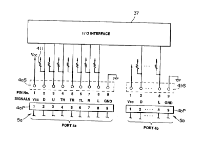
As shown in Fig. 4 the i/O interface has two channels connected
to peripheral ports 4a and 4b. Each of the peripheral ports 4a and
4b has a set of socket pins 1 through 9. Pins 2 through 8 are
connected to I/O interface and assigned to send and receive a set of
specific signals. Names and functions of the signals are shown in
Table 1.
As shown in Fig. 4, each of plugs 4ap and 4bp which are to be
connected to the sockets 4as and 4bs respectively has a set of plug
pins 1 through 9 corresponding to the socket pins 1 through 9. The
plug 4ap and 4bp are connected to main circuits of peripheral
devices via cables 5a and 5b.
- 14 -
WO 96/12250 217 6 9 4 0 p~y~5~02073
Table 1
Signal Narrie Pin No. Remarks
TH 4 Control signal from
game apparatus
TR 5 Control signal from
game apparatus
TL 6 Control signal to
game apparatus(ack)
R 7 Data signal (third
bit)
L 8 Data signal (second
bit)
D 2 Data signal (fi rst
bit)
U 3 Data signal (0-th
bit)
Vcc 1 Power Source(+5V)
Pins nos. 4 to 6 are assigned for control signals. Pin no. 4 is the
first control pin and assigned for transmitting a peripheral
selection signal TH from the game apparatus 2 to the peripheral
device (for example, controllers 3a, 3b). Pin no. 5 is the second
control pin and assigned for transmitting a data request signal TR
from the game apparatus to the peripheral device. Pin no. 6 is the
third control pin and assigned for transmitting a peripheral
acknowledgement signal TL from the peripheral device to the game
apparatus.
Pins nos. 2, 3, 7 and 8 are assigned for data signals. Pin no. 2
(the first data pin) is assigned for transmitting a bit data D, pin no.
- 15 -
2176940
WO 96/12250 PGT/JP95/0207:
3 (the second data pin) for a bit data U, pin no. 7 (the third data pin)
for a bit data R, and pin no. 8 (the fourth data pin) for a bit data L,
respectively. The data R is mainly used for data transmission to
the game apparatus 2. The input/output directions of data for
these signals D, U, R and L can optionally be specified in accordance
with the kind of the peripheral device connected to the apparatus 2.
The signal R represents the third bit of the data, L the second bit, D
the first bit and Uthe 0-th bit, respectively.
Pins 2 through 8 are connected to an electric power source Vcc
by way of resisters 411, respectively, thereby to pull up the
voltage levels of the signal lines (pins nos. 2 to 8) to the level of
the power source Vcc.
When a peripheral device is not connected to the port 4a (4b)
the voltage level on each of pins nos. 2 to 8 is equal to the voltage
value of the power source Vcc (i.e. logical value = binary value "1 ").
Thus, the sub CPU 25 identifies that a peripheral device is not
connected to the socket 4as (4bs) when it receives these data of
the voltage state "1 ", for example, for D, U, R and L.
Pins nos. 5 and 6 are mainly assigned for transmitting control
signals between the game apparatus and the peripheral devices in
the above description. However, pins 5 and 6 may be used for data
signal transmission where a peripheral device employs either the
clocked parallel communication mode or clocked serial
communication mode which wi I I be described below.
Pin no. 1 is assigned to the signal Vcc which represents the
power source (voltage: +5V). The pin no. 9 is assigned to the signal
- 16 -
WO 96/12250 217 6 9 4 0 p~y~s/02073
CND which represent the ground potential (voltage: zero).
Figs. 5A to 5C explain a variety of pin configurations for plugs
4ap and 4bp which very depending on communication modes
employed by peripheral devices. Fig. 5A shows a pin configuration
for standard communication modes including a TH/TR-selection
communication mode and a three-wire handshake communication
mode, Fig. 5B shows a pin configuration for a clocked parallel
communication mode (clock-synchronized-type parallel
communication mode), and Fig. 5C shows a pin configuration for a
clocked serial communication mode (clock-synchronized-type
serial communication mode), respectively. The clocked parallel and
serial communication modes correspond to the non-standard type of
modes.
These pin configurations are prepared to easily comply with a
large number of types of peripheral devices, such as a control PAD,
mouse, key board, modem and memory unit, and with different
communication modes which may change according to peripheral
devices.
Typical communication modes employed by a variety of
peripheral devices are, for example, a TH/TR-selection
communication mode, a three-wire handshake mode, a clocked
parallel mode, and a clocked serial mode. A peripheral device
employing the TH/TR-selection and three-wire handshake
communication modes requires all of the socket/plug pins 1
through 9 of the connector port 4a (4b) to be used electrically
independently. Accordingly, as shown in Fig. 5A, all the pins 1
- 17 -
2176940
wo 96ni2s° rcri~siozo~~
through 9,of the plug 4ap (4bp) are not short-circuited to each
other.
On the other hand, where a peripheral device employs the clocked
paralael communication mode, pin no. 5 assigned for the data '
request signal TR and pin no. 6 assigned for peripheral
acknowledgment signal TL can electrically be short-circuited as
shown in Fig. 5B. Further, in case of a peripheral device employing
the clocked serial communication mode, the data transmission
lines in the connector port 4a (4b) can be reduced to one line in
principle, and it is possible to transmit data through the one data
line in cooperation with the two peripheral selection line (TH) and
data request line (TR). Accordingly, as shown in Fig. 5C, pin no. 2
may be connected to Vcc and pins 6 to 8 may be connected to GND.
As is exemplified above, it is understood that each of the
connector ports 4a and 4b have a certain requirement in the number
of needed signal lines (i.e., pins), which is determined in
accordance with the employed communication mode. The
processing apparatus 2 can use logical values on specified signal
lines (in other words, specified pins) at the connector ports 4a and
4b to decide communication modes. Namely the apparatus 2 can
determine the communication modes according to the logical values
on the signal lines (pins).
Thus, in order to identify the employed communication mode, it
should be essential to know the numbers of pins required to
transmit data and the logical values on each signal line (i.e., each
specified pin). In the present embodiment, the pin configurations
- 18 -
2176940
WO 96/12250 PCT/JP95/02073
~.f the plugs are designed to be able to transmit effectively to the
apparatus 2 the logical values required to decide the
communication mode employed by a peripheral device. In
consequence, the apparatus 2 can quickly decide the employed
communication mode.
Where the communication mode of a peripheral device is
clocked parallel mode, the pin configuration of each-plug 4ap (4bp)
of the connectors are shown in Fig. 5B. In this mode, the apparatus
2 transmits to the controllers 3a and 3b a specified logical value
("1" or "0") as the peripheral selection signal TH and given clock
signals as the data request signal TR. In response to this, signals
of required logical values are then quickly provided through the
data lines from the controllers 3a and 3b in synchronization with
the clock signals. As shown in Fig. 5B, the pin 5 for the data
request signal TR is short-circuited with the pin 6 for the
peripheral acknowledgment signal TL in this clocked parallel
communication mode, thereby the signals (voltages) on both the
plug pins no. 5 and 6 being the same. Accordingly the signal TR
transmitted from the apparatus 2 to pin no. 5 is sent back almost
simultaneously from pin no. 6 to the apparatus 2 as the signal TL.
Thus, the apparatus 2 identifies the clocked parallel mode by
sensing signal TL equal to signal TR.
Further, in case of a peripheral device of the clocked serial
communication mode, only one signal line (U) is required to
transmit data. In addition, only the peripheral selection signal line
(TH) and data request signal line (TR) transmitting clock signals
- 19 -
2176940
WO 96/12250 PCT/JP95/0207:.
are required as control lines. And logical values needed to ident~;fy
this communication mode may be set as R=L="0", D="1", and U="1".
These requirements may be realized by such pin configurations of
the plugs 4ap and 4bp as shown in Fig. 5C in which plug-pins which
are not used for transmitting data and control signals are
connected to fixed potentials (Vcc and GND). For example, pin no. 2
is connected to the power source Vcc and pins nos. 6 to 8 are
connected to the ground GND. This plug-pin configuration-wi I I make
it possible to produce required logical values representing the
clocked serial communication mode at the pins of the plugs 4ap and
4bp, thus such logical values being supplied to the apparatus 2.
The short-circuit between the pins in Figs. 5B and 5C may be
achieved either by putting a short-circuit wire bridging connecting
portions at which the plug pins are connected to the corresponding
wires contained in the cable 5a (or 5b) in the plug or by providing a
short-circuit pattern on a printed circuit board arranged in the plug
4ap (4bp). This reduces in number wires in the cable 5a (or 5b)
connecting the plug 4ap (4bp) to the main circuit of a peripheral
device.
The foregoing short-circuit can be achieved within the main
circuit of a peripheral device either by putting a short-circuit wire
bridging wires of the cable 5a (or 5b) or by forming a specified
short-circuit printing pattern on a printed circuit board. Though
this short-circuit design cannot reduce the cable 5a (or 5b) in
number, the plug can be reduced in size.
Particularly in the case of pin configuration of the plug 4ap
- 20 -
WO 96/12250 217 6 9 4 0 pG.IYJP95ro2073
(4bp) shown in Fig. 5C assigned to the clocked serial
communication mode, the no. 2 pin is short-circuited and
electrically connected to the no. 1 pin (signal Vcc; power source
pin) and the pins nos. 6 to 8 are all short-circuited and electrically
connected to the no. 9 pin (signal GND; ground pin). And accordingly
wires in the cable connecting the plug 4ap (or 4bp) with the main
circuit of a peripheral device can largely be decreased in number,
because only the fines of the data signal U and the control signals
TH and TL are required.
On one hand, when the pin configuration of Fig. 5C is effectively
realized within a peripheral device, the lines of the cable,
independent of signal transmission, are electrically connected to
the power source and the ground potential, which leads to reduced
noises which may fall onto the lines.
The functional and hardware schematic diagrams of controllers
as representatives of peripheral devices employing the foregoing
various communication modes wi I I now be explained, respectively,
with reference to Figs. 6A to 6D and 7A to 7D which use part of the
same reference numerals as ones described above.
Fig. 6A shows a controller 3a employing the TH/TR-selection
communication mode. The controller 3a comprises the plug
connector 4ap, the cable 5a having nine wires connected to the nine
plug pin nos. 1 to 9 of the plug connector 4ap, and a main circuit 3M
to which the wires of the cable 5a are connected. The nine plug pin
nos. 1 to 9 are electrically independent from each other and
individually connected to the nine wires of the cable 5a. The main
- 21 -
2176940
WO 96/12250 PCT/JP9510207:.
circuit 3M has an operating portion 3Ma and a data generator 3Mb.
The operating portion 3Ma, which is operated by a player, includes
keys and/or switches. The data generator 3Mb is formed by
circuits such as hardware logic circuits or a CPU system such that
a specific group of 4-bit data R, L, D, U including data generated at
the operating portion 3Ma are selected from other data groups and
supplied through the plug pin nos. 2, 3, 7, 8 in response to bit
patterns of both the peripheral selection signal TH and data request
signal TR.
One detailed hardware schematic diagram of a controller 3a
employing the TH/TR-selection communication mode is exemplified
in Fig. 7A. As shown therein, the data generator 3Mb consists of a
one chip type logic IC containing buffers and other logic gates such
as AND and NAND gates for carrying out the foregoing operation.
Various key switches arranged on the top cover of the controller 3a
and pushed by a player are connected to the logic IC 3Mb. Among
them are a start key "START", 4-way directional keys "UP(I)",
"DOWN (I)", "LEFT(I)" and "RIGHT(I)", specialized right- and left-
steering keys "T R" and "T L", and other keys "T A" to "T C" and "T X"
to "T Z" assigned for special functions such as jumping and rotation
in a monitor screen. The logic IC 3Mb selects key data of the above
key switches every one group (three keys or four keys are combined
as one group) in response to bit patterns of the 2-bit data selecting
signals TH and TR (i.e., peripheral selection signal TH and data
request signal TR).
Fig. 6B shows a controller 3a employing the three-wire
- 22 -
WO 96/12250 217 6 9 4 0 ~,~.~~5~02073
handshake communication mode. The controller 3a comprises the
plug connector 4ap, the cable 5a having nine wires connected to the
nine plug pin nos. 1 to 9 of the plug connector 4ap, and a main
circuit 3M to which the wires of the cable 5a are connected. The
nine plug pins 1 to 9 are electrically independent from each other
and individually connected to the nine wires of the cable 5a. The
main circuit 3M has an operating portion 3Ma and a CPU system 3Mb.
The CPU system 3Mb has a CPU and functions as a data generator
which is responsive to the operating portion 3Ma. A data generator
formed by hardware logic circuits can be adopted as a substitute
for the CPU system. The CPU system 3Mb communicates with the
game apparatus 2 using the three signals TH, TR, and TL
sequentially inputted or outputted through the plug connector 4ap
and then supplies 4-bit parallel data R, L, D, U including data
generated at the operating portion 3Ma to the game apparatus 2
through the plug connector 4ap. When output signals from an
operating portion 3Ma are analog quantities, the operating portion
3Ma includes signal processing circuits such as an A/D convertor.
For example, one controller 3a employing the three-wire
handshake communication mode is shown in detail in Fig. 7B, which
has a CPU system 3Mb and executing the foregoing signal
processing. The CPU system 3Mb includes IC J1 (part No. 74HC157)
which functions as a selector for selecting ID data. The selector
includes four of 2-inputs/1-output type selecting circuit
connecting to another IC J2 which is a 4-bit microcomputer (CPU).
Various key switches operated in a video game, for instance, which
- 23 -
2176940
WO 96/12250 PCT/JP95/0207.
composes the operating portion 3Ma, are connected to IC J2. Thus
in response to the peripheral selection signal TH and data request
signal TR, the microcomputer not only reply by sending out the
peripheral acknowledgement signal TL but also reads the states of
the key switches, and outputs them as 4-bit data R, L, D, U by way
of IC J1.
Fig. 6C shows a controller 3a employing the clocked parallel
communication mode. The controller 3a also comprises the plug
connector 4ap of nine pin nos. 1 to 9, the cable 5a, and a main
circuit 3M. Among the nine plug pin nos. 1 to 9, the pins of nos. 5
and 6 are short-circuited at their pin portions to each other and the
remaining pins are sti I I electrically independent. The plug pins of
Nos. 1 to 5 and 7 to 9 are coupled with the respective wires of the
cable 5a. The main circuit 3M has an operating portion 3Ma and a
data generator 3Mb which can be constructed using gate array
circuits, for example. The data generator 3Mb, through the plug
connector 4ap, sequentially receives the peripheral selection signal
TH and data request signal TR (potentially equal to the peripheral
acknowledgement signal TL due to the short circuit) and, almost
simultaneously with the reception of the signal TR, supplies to the
game apparatus 2 4-bit parallel data including data generated at
the operating portion 3Ma. The plug pin configuration of this mode
reduces the number of wires of the cable 5a by one, as shown in Fig.
6C. The clocked parallel communication mode permits the game
apparatus 2 to communicate with the controller 3a in the same
manner as the three-wire handshake mode.
- 2 4 --
2176940
WO 96/12250 PCT/JP95/02073
Fig. 7C exemplifies the detailed internal block diagram of a
controller 3a employing the clocked parallel communication mode.
A data generator 3Mb, which consists of gate arrays, plays a key
role for the foregoing operation in the controller 3a. The data
generator 3Mb includes ICs J3, J4 (part No. 74HC74) and IC J5
(74HC14) which play together a key role for generating a 3-bit data
selecting signal supplied to each of four parallel-arranged ICs J6
to J9. ICs J6 to J9 (part No. 74HC151) are selectors of 8-inputs/1-
output type and each arranged to receive key data from each of
four-divided key groups in the key switches of the operating
portion 3Ma. Each of ICs J6 to J9 selects one data (including ID
data or key data) responsibility to bit patterns of the supplied 3-
bit data selecting signal (i.e., address signal). Thus, 4-bit parallel
data R, L, D, U are outputted from ICs J6 to J9.
Fig. 6D shows a controller 3a employing the clocked serial
communication mode. The controller 3a also comprises the plug
connector 4ap of nine pins of nos. 1 to 9, the cable 5a, and a main
circuit 3M. Among the nine plug pins of nos. 1 to 9, the pins of nos.
1 and 2 are short-circuited and the pins of nos. 6 to 9 are short-
circuited, respectively, at their pin portions to each other and the
remaining pins are sti I I electrically independent. The plug pins of
nos. 1, 3 to 5, and 9 are coupled with the respective wires of the
cable 5a. The main circuit 3M has an operating portion 3Ma and a
data generator 3Mb which can be constructed using gate array
circuits, for example. The data generator 3Mb, through the plug
connector 4ap, sequentially receives the peripheral selection signal
- 25 -
2176940
WO 96/12250 PCT/JP95/01073
TH and data request signal TR, and in response to clock pulse
inversion, supplies to the game apparatus 2 serial data including
data generated at the operating portion 3Ma. The plug pin
configuration of this mode remarkably reduces the number of wires
of the cable 5a by four, as shown in Fig. 6D.
Fig. 7D shows one detailed example of a controller 3a employing
the clocked serial communication mode. The controller 3a has a
data generator 3Mb consisting of gate arrays, where included are
ICs J10 to J12 (part No. 74LS166), which are cascade-connected,
are shift registers. IC J10 placed at the first stage are used for
sending ID data in sequence. ICs J11 and J12 placed at the second
and third stages are connected to the key switches of the operating
portion 3Ma and used for sending serial key data U. Thus in
response to the peripheral selection signal TH and data request
signal TR, ICs J11 to J12 sends out ID data and key data in
sequence. This controller 3a has facilities for a cascade
connection of controllers. In other words, there is provided a
circuit J13 for recognizing whether serial data from another
cascade-connected controller are inputted through a socket
connector 4as'.
I n Figs. 6C and 6D, and 7C and 7D, such s h o rt-c i rc a i t
configuration can be achieved in the side of the main circuit 3M.
In the present embodiment, when the plug 4ap (or 4bp)
connected to the controller 3a (or 3b) is inserted into the socket
4as (or 4bs) arranged in the apparatus 2, the foregoing plug pin
configurations permit the sub CPU 25 to communicate to process in
- 26 -
2 1 7 6 9 4 0 pcriJr9sioior3
the order of "peripheral ID-1 ", "peripheral ID-2", "data size", and
"data", even though the controller 3a (or 3b) as the peripheral
device adopts different communication modes or different device
types Also the foregoing plug pin configuration provides the
communication of "peripheral IDs" and "data" in a proper state,
although types and/or communication modes of peripheral devices
are different.
The operation of the apparatus 2 functionally including the
system for identifying communication modes of peripheral devices
wl II now be explained with reference to Figs. 3 to 15 and Table 2 to
6.
As shown in Fig. 8, after being activated, the sub CPU 25 fist
outputs the control signals TH="1" and TR="1" (refer to Step S101
in Fig. 8). The CPU core 31 of the sub CPU 25 reads logical values
of the data signals R, L, D and U produced on pins 7, 8, 2 and 3 by
each of the peripheral devices and stores the read logical values
into a predetermined memory area of the RAM 33 (Step S102). The
CPU core 31 again outputs the control signals TH="0" and TR="1"
(Step S103). In response to this, the CPU core 31 again reads
logical values of the data signal R, L, D and U produced by the
peripheral devices and stores them into a predetermined memory
area of the RAM 33 (Step S104: see the intervals Tao in Fig. 13 and
T2o i n Fig. 14).
The CPU core 31 then calculates the "peripheral ID-1 " (Step
S105). The "peripheral ID-1 " can be calculated using the following
fo rm a la.
_ 27 _
2176940
WO 96/12250 PCT/JP95/02073
[ID-1 J = {(data R in TH="1 ") or (data L in TH="1 ")} x 8h
+ {(data D in TH="1 ") or (data U in TH="1 ")} x 4h
+ {(data R in TH="0") or (data L in TH="0")} x 2h
+ {(data D in TH="0") or (data U in TH="0")} x 1 h
where h represents suffix for hexadecimal number. Using the
calculated results of [ID-1], the CPU core 31 identifies the types of
peripheral devices (Steps S106 to S110). The following table 2
shows a relation between the types of peripheral devices and the
calculated results of [ID-1].
- 28 -
WO 96/12250 217 6 9 4 0 p~y~5~02073
Table 2
Peripheral Device ID-1
F
E
3/6 Button D
C
Control PAD B
A
9
8
Adaptor 7
6
Controller (Peripheral #1 ) 5
4
Mouse
2
1
Modem 0
In detail, the CPU core 31 first determines whether or not the
calculated result [ID-1) is Bh, for instance. When it is determined
that the calculated result [ID-1] be Bh (YES at Step S106), it is
decided that the peripheral device be a control PAD packed together
with the game system. The relation between peripheral devices and
- 29 -
2176940
WO 96/12250 PCT/JP95/0207.
values of ID-1 is shown in Table 2. Thus the CPU core 31 performs
the processing of a control PAD access subroutine (Step S111 ).
When the calculated result [ID-1] is not Bh (NO at Step S106), the
CPU core 31 then determines whether or not the calculated result
[ID-1] is 5h, for example (Step S107).
When it is determined that the calculated result [ID-1] be 5h
(YES at Step S107, also refer to Table 2), a controller access
subroutine is processed (Step S112), which is shown in detail in
Fig. 9.
When the calculated result (ID-1] is not 5h (NO at Step S107),
the sub CPU 25 proceeds to the determination whether the
calculated result (ID-1] is 7h, for example (Step S108). When the
determination is YES at Step S108 (i.e., the calculated result [ID-1]
= 7h), the sub CPU 25 then performs an adaptor access subroutine
(Step S113).
When it is determined that the calculated result [ID-1] be not 7h
(NO at Step S108), the sub CPU 25 continues to determine if the
above calculated result [ID-1] is 3h or not, for example (Step S109).
Where the calculated result [ID-1] is determined to be 3h (YES at
Step S109, Table 2), a mouse access subroutine is processed (Step
S114).
When the above result [ID-1] is not 3h (NO at Step S109), it is
then determined whether or not the calculated result [ID-1] be Dh
(Step S110). Where this determination shows that the calculated
result [ID-ij is Dh (YES at Step S110, Table 2), a 3/6 button access
subroutine is then performed (Step S115). When the determination
- 30 -
wo 96n22so 217 6 9 4 0
PGT/JP95/02073
is NO at Step 110, the processing is continued to Step S116, where
a decision that the peripheral device is not connected is made for
the calculated result [ID-1] = Fh and a decision to be unknown is
made for values of the [ID-1] other than the above exemplified
results (refer to Table 2).
As a representative, the control PAD access subroutine wi I I be
described. In this subroutine, an access to the control PAD is
carried out under the TH/TR-selection communication mode
automatically designated. This communication mode uses 2-bit
data consisting of combined two signals of the peripheral selection
signal TH and data request signal TL to select a group of data
generated in the control PAD. The selected group of data is
supplied from the control PAD to the game apparatus. In the
present embodiment, the TH/TR-selection communication mode is
preferably employed in the control PAD and the 2-bit data can
select four patterns for, for example, four-bit data R, L, D and U.
The table 3 shows a truth values of this mode, in which the
references "RIGHT", "LEFT", "DOWN", "UP", "START", and "TRG-A, B, C,
X, Y, Z, L, R" are names of the key portions and switch portions.
Data of the peripheral acknowledgment signal TL are ignored in the
TH/TR-selection communication mode.
- 31 -
2176940
WO 96/12250 PGT/JP95/020 i.
Table 3
DATA TH TR TL R L D U
bit6 bits bit4 bit3 bit2 bitl bit0
INPUT INPUT OUT- OUT- OUT- OUT- OUT-
PUT PUT PUT PUT PUT
1 st 1 1 1 TRG- 1 0 0
L
2nd 0 1 1 RIGHT LEFT DOWN UP
3rd 1 0 1 STA- TRG- TRG- TRG-
RT A C B
4th 0 0 1 TRG- TRG- TRG- TRG-
R X Y Z
As another representative, the foregoing controller access
subroutine shown in Fig. 9 will now be described also with
reference to Table 4 which represents the bit patterns of data R, L,
D and U corresponding to typical communication modes used by
controllers as peripheral devices.
- 32 -
2176940
WO 96/12250 PCT/JP95/02073
Table 4
Communication TH=1 TR=1 TH=0 TR=1
mode R L D U R L D U
Three-wire 0 0 0 1 0 0 0 1
handshake
Clocked serial 0 0 1 0 0 0 1 0
Clocked parallel 0 0 1 1 0 0 1 1
In this access subroutine, the CPU core 31 of the sub CPU 25
fi rst determines communication modes by a series of Steps S201
to S203 on the basis of the logical values of the data D and U
acquired before. When both the data D is "0" and U is "1" (YES at
Step S201), the peripheral device is identified as in the three-wire
handshake mode (refer to Table 4), and the processing by the sub
CPU 25 proceeds to a three-wire handshake-type access subroutine
(Step S204).
When the data D and U are not "0" and "1 ", respectively (NO at
Step S201), the CPU core 31 then determines whether both of the
data D and U are "1" and "0", respectively, for example (Step S202).
When the determination is YES at Step S202 (i.e., D="1" and U="0",
refer to Table 3), the CPU core 31 continues to an access
subroutine of the clocked serial communication mode (Step S205).
Furthermore, where the determination is NO at Step S202 (i.e.,
data D is not "1" and data U is not "0"), the CPU core 31 determines
whether or not the data D is "1 " and data U is "1 " (Step S203). When
- 33 -
2176940
WO 96/12250 PCT/JP95/0207,
being determined that D="1" and U="1" (YES at Step S203, refer to
Table 4), the CPU core 31 performs an access subroutine of the
clocked parallel communication mode (Step S206).
When the CPU core cannot find the positive answers at any of
the above determination processes at Steps S201 to S203 (NO at
Steps S201 to S203), it is then determined that any peripheral
device be not connected to the apparatus 2 (Step S207), and this
subroutine is ended up.
Each access subroutine shown at the above Steps S204 to S206
wi I I now be explained in detail.
First, the access subroutine of the three-wire handshake
communication mode, which is shown in Fig. 10, wi I I be explained
using the timing chart of each signal shown in Fig. 13 in which the
reference t shows time.
During the interval T» in Fig. 13, the CPU core 31 reads the
"peripheral ID-2" (Step S301 in Fig. 10). In other words, the data
ID-23, ID-22, ID-2~ and ID-2o of R, L, D and U are taken in by the
CPU core 31 during the interval Tii and it is determined whether
each of those data ID-23 to ID-2o corresponds to any of "Oh" to "Fh"
(refer to IDs shown in Table 5).
- 34 -
wo 96nzzso 217 6 9 4 0 p~y~sro2o~3
Table 5
Peripheral Device ID-2 Remarks
Digital device 0 Control PAD,
joystick etc.
Analog device 1 Analog joystick etc.
Pointing device 2 Mouse, tablet etc.
Keyboard 3 Keyboard etc.
Multitap 4 Multitap etc.
5
6
7
9
A
C
D
Peripheral #2 E ID for conversion
fo r non-connection
In addition to the reading, the CPU core 31 looks up Table 5 for
each value of the read peripheral ID-2. For example, the CPU core
31 determines that the peripheral device be a digital device for
"peripheral ID-2" = Oh, an analog device for "peripheral ID-2" = 1h, a
- 35 -
wo ~o . 2 1 7 6 9 4 0
pointing device for 'peripheral ID-2' = 2h, a key board for
'peripheral ID-2' = 3h, and so on.
After such determination, the CPU core 31 reads the data size
during the next interval T~2 (Step S302). Namely, as shown in Fig.
13, data DSIZEO to DSIZE3 of.. R, L, D and U are taken in fo r deciding
the data size.
The CPU core 31 then reads the data during the following
intervals starting from interval T~3 in Fig. 13 (Step S303). It is
then determined whether the amount of the read data reaches the
data size (Step S304). If the determination is NO, the processing
returns to Step S303 to read the data again. However, the
determination is YES at Step S304 (i.e., the data amount that has
been read by then reaches the determined data size), this
subroutine is ended up.
Further, the access subroutine of the clocked parallel
communication mode recited in Fig. 9 will now be explained using
Figs. 11 and 14.
Fig. 14 shows the timing chart of the clocked parallel
communication mode, which is almost the same as that shown in
Fig. 13. Only one difference is that both of the signals TR and TL
always change at the same timing, because of the short-circuit of
pin nos. 5 and 6 in the plug connector 4ap (4bp).
First, the CPU core 31 reads the 'peripheral ID-2' during the
interval T2~ in Fig. 14 (Step S401 in Fig. 11).
in detail, the data ID-23, ID-22, ID-2~ and ID-2o of R, L, D and U
are taken in by the CPU core 31 during the interval T2~ and it is
- 36 -
2176940
WO 96/12250 PCT/JP95/02073
determined whether each of the data ID-23 to ID-2o corresponds to
any of "Oh" to "Fh" (refer to IDs shown in Table 5). The CPU core 31
looks up Table 5 for each value of the read peripheral ID-2. For
example, the CPU core 31 determines that the peripheral device be
a digital device for "peripheral ID-2" = Oh, an analog device for
"peripheral ID-2" = 1h, a pointing device for "peripheral ID-2" = 2h,
a key board for "peripheral ID-2" = 3h, and so on.
After this, during the next interval T22, the CPU core 31 reads
the data size by receiving data DSIZEO to DSIZE3 of R, L, D, U as
shown i n Fig. 14 (Step S402 i n Fig. 11 ) .
The CPU core 31 then reads the data during the following
intervals starting from interval T23 in Fig. 14 (Step S403). It is
then determined whether the amount of the read data reaches the
data size (Step S404). If the determination is NO, the processing
returns to Step S403 to read the data again. However, the
determination is YES at Step S404 (i.e., the data amount that has
been read by then reaches the determined data size), this
subroutine is ended up.
Further, the access subroutine of the clocked serial
communication mode wi I I be explained according to Figs. 12 and 15
and Table 6. Fig. 15 exemplifies signal changes for the clocked
serial mode, where the logical values of only the signals TH, TR and
U are expressed along the elapsed time t.
This communication mode enables to obtain the data U only
supplied from a peripheral device when the peripheral selection
signal TH is "0" and at the same time, the data request signal TR is
- 37 -
2176940
WO 96/12250 PCT/JP95/020?,
repeatedly "1" and "0", both the signals TH and TR being given to the
peripheral device from the CPU core 31. The obtained data are
exemplified in Table 6.
Table 6
TH TR TL R L D U Remarks
(input)(input)(GND) (GND) (GND) (Vcc) (DATA)
1 1 0 0 0 1 0 ID-1 (1 st)
0 1 0 0 0 1 0 ID-2(2nd)
0 ~. T 0 0 0 1 SMD3
0 ,~ T 0 0 0 1 SMD2
0 ~. T 0 0 0 1 SMD~
0 ,~ '~ 0 0 0 1 SMDo
0 ,~ T 0 0 0 1 ID-23
0 ~. T 0 0 0 1 I D-22
0 ~ T 0 0 0 1 ID-2i
0 ~. T 0 0 0 1 I D-2o
0 j T 0 0 0 1 DSIZE3
0 ,~ T 0 0 0 1 DSIZE2
0 ~. T 0 0 0 1 DSIZE~
0 ~. T 0 0 0 1 DSIZEo
0 ~. T 0 0 0 1 DATA?
0 ,~ T 0 0 0 1 DATAo
- 38 -
wo 96/i22so 217 6 9 4 0
PCT/JP95/02073
0 ~. T 0 0 0 1 CCB
0 ~. T 0 0 0 1 1
0 ~. T 0 0 0 1 1
0 ~. T 0 0 0 1 0
1 1 0 0 0 1 0 End M51D-1 st
As shown in Table 6, only when the peripheral selection signal
TH is "0", the data request signal TR is repeated at cycles of "1" and
"0" (expressed by upward and downward arrows in Table 6), the
signal TL and data R and L are all "0", and the data D is "1 ", various
data U including SMD3 to SMDo, ID-23 to ID-2o, DSIZE3 to DSIZEo, and
DATA to DATAo are provided in sequence from the line U through
the pin 3. Those data are read by the CPU core 31. Among them, the
bit pattern of the data ID-23 to ID-2o are referred to the table 5 to
decide the type of a connected peripheral device (Step S501 in Fig.
12).
The CPU core 31 reads the data size expressed by DSIZEo to
DSIZE3 (Step S502), so that the data size can be determined.
The data are then received by the CPU core 31 during
predetermined intervals in a time sequence shown in Fig. 15 (Step
S503). The amount of the read data are referred to the determined
data size to determine whether the amount reaches the data size
(Step S504). If the determination is NO, the processing returns to
Step S503 to repeat the foregoing data read. The determination of
YES at Step S504 allows to end up this subroutine.
- 39 -
2176940
WO 96/12250 PCT/JP95/0207
As having been explained, the CPU core 31 exchanges signals
with peripheral devices such that data "DATA" are inputted after
information of "peripheral ID-1 ", "peripheral ID-2" and data size
"DSIZE".
When the data are inputted into the CPU core 31, the CPU core
31 is to exchange data with the main CPU 21 through the register
table 34.
In the above embodiment, although the sub CPU 25 controls the
peripheral devices, the main CPU 21 can also perform the above-
described processing instead of the sub CPU 25, if the main CPU 21
is directly connected to the peripheral devices.
Further, another identifying method of a communication mode
can be used in the present invention. As is described above, the
control signals TR and TL are equal in logical values (TR = TL) in
the clocked parallel communication mode and the logical values on
only specified pins (D, TL, R, L) are changed in specific manners. In
case of the three-wire handshake mode, the control signals TR and
TL are changed differently. This enables to calculate identification
data of peripheral devices based on the pin configurations of the
connectors and decide communication modes using the
identification data.
Although the present invention has been described with
reference to particular embodiments, the description is only an
example of the invention's application and should not be taken as a
limitation. In particular, the connector, the communication mode
identifying system, and the peripheral device controlling system of
- 40 -
WO 96112250 21 l 6 9 4 0 p~y~5~02073
the present invention is not limited to use with the game apparatus
and can also be applied to any other system which use a processing
unit and at least one peripheral device thereof.
- 41 -