Note: Descriptions are shown in the official language in which they were submitted.
CA 02176945 1999-10-13
WO 96/10879 PCT/US95109774
METHOD AND APPARATUS FOR
COHERENT COMMUNICATION RECEPTION IN A
SPREAD-SPECTRUM COMMUNICATION SYSTEM
This application is a continuation-in -part of U.S. Patent No.
5,659,573 issued August 19, 1997.
Field of the Invention
15
The present invention relates to communication systems which
employ spread-spectrum signals and, more particularly, to a method and
apparatus for coherent communication reception in a spread-spectrum
communication system.
Background of the Invention
Communication systems take many forms. One type of
communication system is a multiple access spread-spectrum system. In
a spread-spectrum system, a modulation technique is utilized in which a
transmitted signal is spread over a wide frequency band within the
communication channel. The frequency band is much wider than the
minimum bandwidth required to transmit the information being sent. A
voice signal, for example, can be sent with amplitude modulation (AM) in
a bandwidth only twice that of the information itself. Other forms of
modulation, such as low deviation frequency modulation (FM ) or single
sideband AM , also permit information to be transmitted in a bandwidth
comparable to the bandwidth of the information itself. However, in a
spread-spectrum system, the modulation of a signal to be transmitted
often includes taking a baseband signal (e.g., a voice channel) with a
bandwidth of only a few kilohertz, and distributing the signal to be
transmitted over a frequency band that may be many megahertz wide.
This is accomplished by modulating the signal to be transmitted with the
information to be sent and with a wideband encoding signal.
Three general types of spread-spectrum communication
2176945
WO 96!10879 PC1'IUS95/09774
-2_
techniques exist, including direct sequence modulation, frequency and/or
time hopping modulation, and chirp modulation. In direct sequence
modulation, a carrier signal is modulated by a digital code sequence
whose bit rate is much higher than the information signal bandwidth.
Information (i.e. the message signal consisting of voice and/or
data) can be embedded in the direct sequence spread-spectrum signal
by several methods. One method is to add the information to the
spreading code before it is used for spreading modulation. It will be
noted that the information being sent must be in a digital form prior to
adding it to the spreading code, because the combination of the
spreading code and the information, a binary code, typically involves
modulo-2 addition. Alternatively, the information or message signal may
be used to modulate a carrier before spreading it.
These direct sequence spread-spectrum communication systems
can readily be designed as multiple access communication systems. For
example, a spread-spectrum system may be designed as a direct
sequence code division multiple access (DS-CDMA) system. In a DS-
CDMA system, communication between two communication units is
accomplished by spreading each transmitted signal over the frequency
band of the communication channel with a unique user spreading code.
As a result, transmitted signals are in the same frequency band of the
communication channel and are separated only by unique user
spreading codes. These unique user spreading codes preferably are
orthogonal to one another such that the cross-correlation between the
spreading codes is approximately zero.
Particular transmitted signals can be retrieved from the
communication channel by despreading a signal representative of the
sum of signals in the communication channel with a user spreading code
related to the particular transmitted signal which is to be retrieved from
the communication channel. Further, when the user spreading codes are
orthogonal to one another, the received signal can be correlated with a
particular user spreading code such that only the desired user signal
related to the particular spreading code is enhanced while the other
signals for all of the other users are not enhanced.
It will be appreciated by those skilled in the art that several
SUBSTITUTE SHEET (RULE 26~
2176945
~VO 96!10879 PCTIUS95109774
-3-
different spreading codes exist which can be used to separate data
signals from one another in a DS-CDMA communication system. These
spreading codes include but are not limited to pseudonoise (PN) codes
and Walsh codes. A Walsh code corresponds to a single row or column
of the Hadamard matrix.
Further it will be appreciated by those skilled in the art that
spreading codes can be used to channel code data signals. The data
signals are channel coded to improve performance of the communication
system by enabling transmitted signals to better withstand the effects of
various channel impairments, such as noise, fading, and jamming.
Typically, channel coding reduces the probability of bit error, and/or
reduces the required signal to noise ratio usually expressed as error bits
per noise density (i.e., EeINo which is defined as the ratio of energy per
information-bit to noise-spectral density), to recover the signal at the cost
of expending more bandwidth than would otherwise be necessary to
transmit the data signal. For example, Walsh code words can be used to
channel code a data signal prior to modulation of the data signal for
subsequent transmission. Similarly PN spreading codes can be used to
channel code a data signal.
However, channel coding alone may not provide the required
signal to noise ratio for some communication system designs which
require the system to be able to handle a particular number of
simultaneous communications (all having a minimum signal to noise
ratio). This design constraint may be satisfied, in some instances, by
designing the communication system to coherently detect transmitted
signals rather than using non-coherent reception techniques. It will be
appreciated by those skilled in the art that a coherent receiver requires
less signal to noise ratio (in Eb/No) than that required by a non-coherent
receiver having the same bit error rate (i.e., a particular design constraint
denoting an acceptable interference level). Roughly speaking, there is a
three decibel (dB) difference between them for the Rayleigh fading
channel. The advantage of the coherent receiver is more significant
when diversity reception is used, because there is no combining loss for
an optimal coherent receiver while there is always a combining loss for a
noncoherent receiver.
SUBSTITUTE SHEET (RULE 26)
2176945
WO 96110879 PCT/US95/09774
One such method for facilitating coherent detection of transmitted
signals is to use a pilot signal. For example, in a cellular communication
system the forward channel, or down-link, (i.e., from base station to
mobile unit) may be coherently detected, if the base station transmits a
pilot signal. Subsequently, all the mobile units use the pilot channel
signal to estimate the channel phase and magnitude parameters.
However, for the reverse channel, or up-link, (i.e., from mobile to base
station), using such a common pilot signal is not feasible. As a result,
those of ordinary skill in the art often assume that only non-coherent
detection techniques are suitable for up-link communication.
A solution for the need for a coherent up-link channel is found in
U.S. Patent No. 5,329,547 to Fuyun Ling, commonly assigned together
with this application to Motorola, Inc. This patent discloses the
introduction of reference bits into the information datastream prior to
7 5 spreading and transmission, and the subsequent extraction of these
reference samples and their use in forming an estimate of the channel
response. This estimated channel response is in tum used to coherently
detect estimated data symbols.
lNhile this solution allows for coherent detection, it assumes that
more or less standard synchronization and rate detection techniques are
used. However, such techniques do not take advantage of the known
synch pattern, and there are additional impairments to receiver
pertormance that might be improved, if advantage could be taken of this
known synch pattern. Among such problems are frequency offsets, "fat"
finger fading, and n/4 QPSK (quaternary phase shift keying)
synchronization. Frequency offsets may arise, for example, from the
transmitter/receiver clock not being perfectly locked due to inaccuracies
in the crystal oscillator, as well as from large Doppler frequency shifts
(such as from vehicles moving at high speeds in open spaces). A "fat"
finger is a finger of a demodulator circuit that straddles more than one ray
having less than a chip of differential delay; where a "fat" finger occurs
without some form of compensation, it is possible for the finger to center
on the weaker ray, with consequent degradation in signal quality.
Further, if rate detection is either limited to only those frames always
occupied under all speech rates (i.e., frames energized during 1/8th rate
SUBSTITUTE SHEET (RULE 26)
.WO 96/10879 217 6 9 4 5 p~~gg5109774
-5-
speech coding), or is performed on all frames there is a greater likelihood
of an erroneous rate determination, ultimately degrading both signal
acquisition and channel estimation. There thus remains a need for an
improved coherent communication system which compensates for these
and other problems.
Brief Description of the Drawings
FIG. 1 is a block diagram showing a preferred embodiment
communication system in accordance with the present invention.
FIG. 2 illustrates a preferred embodiment communication channel
frame structure for use with the communication system shown in FIG. 1.
FIG. 3 is a block diagram showing a preferred embodiment
receiver front end and sampler far use in the receiver shown in FIG. 1.
FIG. 4 is a block diagram showing a preferred embodiment
demodulation circuitry for use in the receiver shown in FIG. 1.
FIG. 5 is a block diagram showing a second embodiment
demodulation circuitry for use in the receiver shown in FIG. 1.
FIG. 6 is a block diagram showing a preferred embodiment buffer
and timing control for use in the receiver shown in FIG. 1.
FIG. 7 is a block diagram showing a preferred embodiment power
estimator and timing control circuitry for use in the receiver shown in FIG.
1.
FIG. 8 illustrates a communication channel frame structure at
different rates for use in the communication system shown in FIG. 1.
FIG. 9 is a block diagram showing a preferred embodiment rate
estimation and channel estimation circuitry for use in the receiver shown
in FIG. 1.
FIG. 10 is a flow chart illustrating a preferred embodiment method
_ for rate estimation and channel estimation in the receiver shown in FIG.
1.
FIG. 11 illustrates a received signal and filtered segments thereof
when using the rate estimation approach of FIG. 10.
FIG. 12 is a chart illustrating a comparison of channel estimation
SUBSTITUTE SHEET (RULE 261
2176945
WO 96110879 PCTIU895/09774
-6-
outputs in the receiver shown in FIG. 1.
FIG. 13 is a chart illustrating a comparison of timing estimation
outputs in the receiver shown in FIG. 1.
Detailed Description
In the course of the following discussion, an improvement for up-
link DS-CDMA communication is presented. This approach employs
coherent detection with reference-symbol based channel estimation, and
in particular employs improved timing, frequency and rate estimation
techniques to optimally detect the received signal. It will be appreciated
by those skilled in the art that other types of communication systems (e.g.,
personal communication systems, trunked systems, satellite
communication systems, data networks, and the like) may also be
adapted and/or designed to use the principles described herein. It has
already been shown that a substantial gain in signal quality (E~/No)can
be obtained relative to non-coherent detection techniques by applying a
coherent detection method to up-link DS-CDMA communication; the
improvements discussed below provide even greater performance gains
through enhanced synchronization and channel estimation of the
receiver.
In order to perform effective coherent detection, it is necessary to
obtain an accurate channel estimate. There are basically two types of
channel estimation methods: data-based and reference-based. Data-
based channel estimation may be implemented as decision-directed or
non-decision-directed. For DS-CDMA up-link communication, the
channel estimator must operate at low signal-to-noise ratios and the
fading is relatively fast. As a result, the decision-directed approach is not
appropriate due to the high decision error rate. On the other hand, a
non-decision-directed method, such as the one described in the article
by A. J. Viterbi and A. M. Viterbi, "Nonlinear Estimation of PSK-Modulated
Carrier Phase with Application to Burst Digital Transmission," IEEE
Trans. on Info. Theory, Vol. IT-29, No. 4, pp. 543-551, Jul. 1983, always
has a phase ambiguity, e.g., 180° ambiguity for binary phase shift key
SUBSTITUTE SHEET (RULE 26~
2176945
.WO 96/10879 PCT/U595/09774
-7- ,
(BPSK) signaling or 90° ambiguity for quaternary phase shift key (QPSK)
signaling, in the channel estimate. As a consequence, it is necessary to
use differential coding to eliminate its effect. However, as will be
appreciated by those skilled in the art, in communication systems having
a differential coded signal transmitted over Rayleigh fading channels,
even with coherent detection, still need over 3 dB higher Ee/No than non-
differentially coded phase shift keying (PSK) signaling.
One way to solve the decision error and phase ambiguity problem
is to use reference symbols for channel estimation. Reference-symbol-
based channel estimation is described as follows. Reference symbols
known to the receiver are inserted into a sequence of information bearing
data bits, which may be coded symbols. At the receiver, the received
signal samples corresponding to the reference symbols are used to
generate a channel estimate. Because the reference symbols are known
to the coherent direct-sequence spread spectrum receiver, there are no
decision errors and the resulting channel estimate does not have a
phase ambiguity. As a result, a robust communication system with non-
differentially coded signaling is provided.
The inserted reference symbols can be organized in blocks or
uniformly distributed. For a flat fading channel, it is desirable to insert
reference symbols periodically and uniformly in the data stream. For a
DS-CDMA up-link with a RAKE receiver for frontend processing, we can
treat the output of each RAKE "finger" as being a flat faded signal. Thus,
the preferred embodiment communication system will uniformly insert
one reference symbol for every M coded data symbols.
The basic operation of RAKE receivers are described in an article
by R. Price and P.E. Green, Jr., "A Communication Technique for
Multipath Channels," Proceedings of the IRE, March 1958, pages 555-
570. Briefly, a RAKE receiver performs a continuous, detailed
measurement of the multipath characteristic of a received signal. This
knowledge is then exploited to combat the selective fading by detecting
signal from each path individually, using a correlation method, and
algebraically combining those echo signals into a single detected signal.
Referring now to FIG. 1, a system for coherent communication in a
spread-spectrum communication system is shown. In order to provide a
SUBSTITUTE SHEET (RULE 26)
WO 96110879 217 6 9 4 ~ PCT/US95I09774
_g_
better understanding of the preferred embodiment receiver disclosed
below, a description of a preferred transmitter that can be
advantageously used with such a receiver will be discussed first.
Beginning with the encoding and interleaving portion 104 of a .
transmitter 101 of the communication system, traffic channel data bits
102 are input to an encoder at a particular bit rate (e.g., 9.6
kilobit/second). The input traffic channel data bits may include voice
converted to data by a vocoder, pure data (including video), a
combination of the two types of data, etc. The encoder encodes the input
data bits 102 into data bits at a fixed encoding rate (1/r) with an encoding
algorithm which facilitates subsequent maximum likelihood decoding of
received data samples into data bits (e.g. convolutional or block coding
algorithms). For example, the encoder encodes input data bits 102 (e.g.,
192 input data bits that were received at a rate of 9.6 kilobits/second) at a
fixed encoding rate of one data bit to three coded data bits (i.e., 1/3) such
that the encoder outputs data bits, e.g., 576 data bits output at a 28.8
kilobit/second rate. These data bits are then input into an interleaver
which organizes the data bits into blocks (i.e., frames) and block
interleaves the input data bits. In the interleaver, the data bits are
individually input into a matrix which defines a predetermined size block
of data bits. The data bits are input into locations within the matrix so that
the matrix is filled in a column by column manner. The data bits are
individually output from locations within the matrix so that the matrix is
emptied in a row by row manner. Typically, the matrix is a square matrix
having a number of rows equal to the number of columns; however, other
matrix forms can be chosen to increase the output interleaving distance
between the consecutively input non-interleaved data bits. The
interleaved data bits 110 are output by the encoder/interleaver 104 at
the same data bit rate that they were input to the interleaver (e.g., 28.8
kb/s (kilobits/second)). The predetermined size of the block of data bits
defined by the matrix is derived from the maximum number of data bits
which can be transmitted at a coded bit rate within a predetermined
length transmission block. For example, if data bits are output from the
encoder at a 28.8 kilobits/second rate, and if the predetermined length of
the transmission block is 20 milliseconds, then the predetermined size of
SUBSTITUTE SHEET (RULE 26J
2176945
~'O 96110879 PCTII1S95/09774
_g_
the block of data bits is 28.8 kilobits/second times 20 milliseconds which
equals 576 data bits which defines an 18 by 32 matrix.
The interleaved data bits 110 are then input to a reference bit
inserter 112 which inserts L known reference bit pairs (generated by
synch bit generator 111, which receives rate information 105 from the
vocoder, in the illustrated case via encoder 104) for every M interleaved
data bit pairs 110. To simplify the following discussion, it will be
assumed that L=1 and M=3 (as is illustrated in FIG. 2), making a four
symbol group. It will be appreciated by those skilled in the art that L and
M could be any value without departing from the scope and spirit of the
present invention. In a preferred embodiment, the inserted reference bits
will have values so as to form predetermined sequences from which a
receiver can determine the appropriate rate information. Thus, for
example, when using an IS-95-like structure of 16 power control groups
of 24 symbols each per frame, together with the reference bit structure of
the present invention (e.g., each power control group having 6 segments
each of 1 reference symbol (L=1 ) and 3 data symbols (M=3, where M is
the number of data bit pairs between reference bit pairs), the following
sequences could be used: 1 ) for full rate, insert reference symbols (r0
through r95, i.e. all symbols (6 each) for the 16 power control groups) the
value 1+ j (=r0); 2) for half rate, insert symbols = r0 in the first and ninth
groups, even symbols = rp and odd symbols = -r0 in the third, fifth,
seventh, eleventh, thirteenth and fifteenth groups, and all remaining
symbols = X (where X means "don't care" since these groups are not
transmifted); and 3) for eighth rate, insert even symbols = rp and odd
symbols = -rp in the first and ninth groups, and all remaining symbols = 0.
If randomization of the power group positions were employed, a mapping
in sequence of the energized groups to those selected by the
randomization can be readily accomplished. (IS-95 randomization
requires that possible eighth rate groups used be a subset of possible
quarter rate groups be a subset of possible half rate groups, such as is
illustrated in FIG. 8). One skilled in the art will appreciate that different
sequence families may be employed, and such may also be extended if
additional information messages are to be sent. Thus, for example, if a
further information bit B (e.g., a power control bit, or received frame error
SUBSTITUTE SHEET (RULE 26~
2176945
WO 96110879 PCTlUS95/09774
_10_
rate at the transmitting unit 101 ) is to be sent per frame, a first reference
sequence family could be used (such as that described above) for B = 0.
If B= 1, the additional sequences could be used: 1) for full rate, all
symbols = r0 in the odd (1, 3...15) groups, and =-r0 in the even (2, 4...16)
groups; 2) for half rate, the same sequence is used as in full rate except
for groups 3, 7, 11, and 15, in which the group reference symbol pattern
is rhalf = {ro ro ro -ro -ro -ro}; 3) for quarter rate, groups 5 and 13 are
assigned the pattern rhait while groups 1 and 9 remain as before; and 4)
for eighth rate, groups 1 and 9 are also assigned the pattern rhaif. While
the probability of transmitting B correctly under full rate remains high
(Pr{error}<10% may be acceptable for this purpose), the probability of
error is higher for lower rates since the sequences are not maintained at
zero crosscorrelation at the lower rates.
When L=1 and M=3, reference bit inserter 112 outputs 768
reference-coded bits 114 for each block (i.e., frame) such that two
reference bits are inserted between each group of six data bits. An
example of a block (i.e., frame) of reference-coded data bits 114 ready
for spreading consisting of 48 bits is shown in FIG. 2 (where each d
represents a data bit and each r represents a reference bit).
The reference-coded data bits 114 are input to a modulating
portion 116 of the communication system. The data bits 114 are
received into a buffer 118, from which the real and imaginary portions of
the bitstream are subsequently read out and separately spread with a
Walsh code Wj and PN code sequences PNi via multipliers 120-121.
Alternatively, a differing code sequence PNi and PNq may be used for
the real and imaginary branches. When the same PNi code is used for
both real and imaginary datastreams, the Walsh code serves as a user
specific sequence of symbols or unique user code. The reference-coded
datastream arrives at modulating portion 116 at a rate of 38.4
kilobits/second. Each section of 6 groups (i.e., 3 pair (a pair making 1
QPSK symbol) of data bits, 1 pair of reference bits x 6 groups = 48 bits) is
then spread so as to output a single 64 symbol length code per input
symbol at a higher fixed symbol rate (e.g., 1228.8 kilosymbols/second,
also referred to as 1.2288 Megachips/second). It will be appreciated by
those skilled in the art that the reference bits and data bits within the
SUBSTITUTE SHEET (RULE 26~
. W O 96!10879 2 l 7 6 9 4 5 PCT~S95109774
-11-
stream of reference-coded data bits 114 may be spread according to
numerous other algorithms into a sequence of larger length codes
without departing from the scope and spirit of the present invention.
For ~rJ4 QPSK modulation the spread symbol stream is then
rotated via multiplier 122 by ~r/4 every chip; for alternative modulations
like QPSK this step is omitted. The symbol streams are then FIR (finite
impulse response) filtered to reduce out of band energy below a set
value, converted to an analog signal stream, and further low pass filtered
via filter/DACs (digital to analog converters) 124, 125. After being
converted to an analog signal the signals from the two symbol streams
are quadrature modulated and summed via multipliers 126, 127 and
summer 128; alternatively, the signals could be combined via direct
digital synthesis. Finally, the modulated signal is amplified by LPA
(linear power amplifier) 129 and provided to antenna 130 for
transmission over the communication channel 131.
The preferred embodiment receiver 135 of the communication
system receives the transmitted spread-spectrum signal from over the
communication channel 131 through antenna 137. The received
reference symbol coded spread spectrum signal is filtered and
downconverted by an analog frontend 139, and inputted to demodulator
circuitry 140. Antenna 136 and demodulator 138 are similarly provided
for space diversity reception of the signal.
The spread spectrum signal is next sampled into despread
samples 148 by despreader and sampler 146. These samples 148
include both reference and data samples, so a reference sample
extractor 150 is used to separate the reference sample information from
the data signal samples. The reference samples 152 are output to a
channel estimator 154, while the remaining data samples 158 from the
despread sampled signal 148 are output to a coherent detector 160 for
later coherent detection of data symbols 162 from the data samples 158.
Finally, the detected data symbols 162-164 are summed in summer
180 with detected data symbols from other fingers or diversity paths and
output to the decoding portion 182 of the communication system.
The despreader and sampler 146 preferably samples the
received spread-spectrum signal at a predetermined rate (e.g., 1.2288 x
SUBSTITUTE SHEET (RULE 26)
2176945
R'O 96110879 PC1'IUS95109774
_12_
8 = 9.8304 Megasampleslsecond). Subsequently, the sampled signal is
decimated to 1.2288 Megasampleslsecond and despread by correlating
the received sampled signals with the spreading code. The resulting
despread sampled signal 148 is sampled at a predetermined rate and
output to the reference sample extractor 150 (e.g., 19.2
kilosamples/second so that a sequence of 64 samples of the received
spread-spectrum signal is despread to and/or is represented by a single
data sample).
The reference sample extractor 150 preferably extracts the
reference samples 152 from the despread sampled signal 148 and
outputs the reference samples 152 to a channel estimator 154. The
data samples 158 from the despread sampled signal 148 are output to a
coherent detector 160 for later coherent detection of data symbols.
However, a problem may arise if the channel estimator 154 output
is used in conjunction with only standard synchronization methods. In
this case the rate of phase rotation of the received signal may be as high
as several kilohertz, impairing signal acquisition. In order to provide
improved synchronization and acquisition, the reference samples 152
and data samples 158 are also input to a synchronization device,
preferably including frequency offset estimator 172 and a timing control
176. To further improve the quality of the synchronization and channel
estimation, a rate estimator 171 determines the rate at which the
encoded data was sent (e.g., full, half or eighth rate) from demultiplexed
reference samples 151 (explained below), and outputs rate estimate
173 at the end of each received frame to the frequency offset estimator
172 and timing control 176, as well as the channel estimator 154. This
use of the rate estimator permits one to use all slots or power control
groups of the frame that are energized, rather than just the slots that are
energized for all rates, to derive the other estimates. The frequency offset
estimator 172 derives an estimate of an offset frequency, such as might
be caused by large Doppler shifts or an imprecise oscillator, which
estimate drives a frequency locked loop to send a control signal 177 to
adjust the frequency of a local oscillator, digital phase corrector (rotator)
or similar circuit of the analog frontend 139 or sampler/despreader 146.
This permits the residual frequency offset to be locked-in at less than 50
SUBSTITUTE SHEET (RULE 26)
2176945
~VO 96110879 PCTlUS95/09774
-13-
f'
Hz (Hertz), greatly improving signal acquisition and detection. Additional
performance gains are provided by the timing control 176 which derives
and combines power estimates of the reference and data signals 152,
158 (that may be unbiased), and then are differenced and filtered and
input to a delay locked loop to control timing so as to center the finger on
the long term average mean ray arrival time. A fast timing (i.e., typically
less than one chip) correction is also achieved by comparing the timing
difference outputs of multiple timing branches and picking the branch
having the maximum value, enabling demodulation to follow the peak
power. This correction is accomplished by controlling a gate 179 via a
fast timing compensation signal 178. The timing control 176, frequency
offset estimator 172, gate 179 and their operations are described in
more detail in connection with FIGS. 3 though 7 below.
Finally, the channel estimator 154 filters the phase rotated,
extracted reference samples 152 of the selected timing branch with a
filter based upon the rate estimate to obtain unbiased, but noisy, channel
estimates. In order to obtain a better channel estimate 156, these noisy
estimates may be passed through a low-pass filter, which may be fixed or
adaptive, to remove the high frequency noise components. The resulting
channel estimates 156 are relatively noise-free and can be used for
coherent detection. It should be noted that the low pass filtering only
gives us a channel estimate for every (M+1 )T, where M is the number of
data bit pairs between each reference bit pair inserted by reference bit
inserter 112 (e.g., M=3) and where T is the time interval of each data bit
pair (or symbol, for QPSK). To perform coherent detection of transmitted
data samples, we need to have a channel estimate for every T. When
(M+1)T is short relative to the channel variation time constant, a simple
but effective method to get a channel estimate for every T is to perform
linear interpolation between two channel estimates separated by (M+1)T.
However, as will be appreciated by those skilled in the art more
- sophisticated interpolation techniques may be used if necessary.
In the preferred embodiment coherent communication system,
power control may also be used to enhance overall system performance.
The power control algorithms may be very similar to the algorithms used
in non-coherent communication systems. The preferred embodiment
SUBSTITUTE SHEET (RULE 26~
2176945
WO 96!10879 PCTlUS95109774
-14-
power control algorithm preferably includes estimating received power
every 1.25 ms (milliseconds) (i.e., each time slot or power control group),
or every 6 reference information samples, i.e., every 18 encoded data
samples or 24 total received signal samples. The power estimate may ,
be calculated with several different techniques. One technique is to
compute a channel estimate with a power estimator 146 simply using the
6 reference signal samples (i.e., reference samples 152 from reference
sample extractor 150) in each 24 sample length group. The square of
the magnitude of the channel estimate is then output by the power
estimator 166 as the power estimate 168.
After channel estimates 156 are generated, the rest of the receiver
is conventional. The coherent detector 160 multiplies the remaining
data samples 158 from the despread sampled signal 148 by the
conjugate of the channel estimates 156 to generate coherently detected
symbols 162.
As will be appreciated by those skilled in the art, multiple receiver
branches 138, 140 and antennae 136, 137, respectively, may be
employed to achieve improved reception through space diversity. All N
diversity receiver branches would operate in substantially the same
manner to retrieve data samples from the received spread-spectrum
signal in communication channel 131 as the above described receiver
branch 140. The outputs 162 through 164 of the N receiver branches
preferably are input to an adder 180 which diversity combines the input
data symbols into a composite stream of coherently detected data
symbols 181.
The individual data symbols 181 which form soft decision data are
then input into a decoding portion 182 including a deinterleaver which
deinterleaves the input soft decision data (i.e., detected data symbols)
181 at the individual data level. In the deinterleaver, the soft decision
data 181 are individually input into a matrix which defines a
predetermined size block of soft decision data. The soft decision data
are input into locations within the matrix so that the matrix is filled in a
row
by row manner. The deinterleaved soft decision data are individually
output from locations within the matrix so that the matrix is emptied in a
column by column manner. The deinterleaved soft decision data are
SUBSTITUTE SHEE7 (RULE 26)
2176945
~ WO 96/10879 PCT/US95109774
-15-
output by the deinterleaver at the same rate that they were input (e.g.,
28.8 kilometricslsecond). The predetermined size of the block of soft
decision data defined by the matrix is derived from the maximum rate of
sampling data samples from the spread-spectrum signal received within
the predetermined length transmission block.
The deinterleaved soft decision data is then input to a decoder
which uses maximum likelihood decoding techniques to generate
estimated traffic channel data symbols 185. The maximum likelihood
decoding techniques may be augmented by using an algorithm which is
substantially similar to a Viterbi decoding algorithm. The decoder uses a
group of the individual soft decision data to form a set of soft decision
transition metrics for use at each particular time state of the maximum
likelihood sequence estimation decoder. The number of soft decision
data in the group used to form each set of soft decision transition metrics
corresponds to the number of data bit pairs at the output of the
convolutional encoder 104 generated from each input data bit 102. The
number of soft decision transition metrics in each set is equal to two
raised to the power of the number of soft decision data in each group.
For example, when a 1/3 convolutional encoder is used in the transmitter
101, three data bits are generated from each input data bit 102. Thus,
decoder 182 uses groups of three individual soft decision data to form
eight soft decision transition metrics for use at each time state in the
maximum likelihood sequence estimation decoder. The estimated data
symbols 185 are generated at a rate related to the rate that the soft
decision data are input to the decoder and the fixed rate used to
originally encode the input data bits 102 (e.g., if the soft decision data
are input at 28.8 kilometrics/second and the original encoding rate was
113 then estimated data symbols 185 are output at a rate of 9640
bits/second). While this information can be used in determining the
occupancy of the various time slots within each frame, in the preferred
embodiment this information is already supplied by the rate estimator
171 described in FIG. 9 below.
Turning now to FIGS. 3 through 7, a more detailed description of a
preferred embodiment of the receiver 135 is illustrated. For purposes of
clarity, only one numeral is used to identify each element appearing in
SUBSTITUTE SHEET (RULE 26)
2176945
WO 96110879 PCTIU595109774
-16-
more than one figure. One skilled in the art will recognize that the
embodiment illustrated is specifically designed for a zr/4 QPSK (or QPSK
if zero rotation) modulated signal. However, the present invention is not
limited in application to OPSK signal reception, but may apply to any
modulated signal that can be coherently received, including but not
limited to OQPSK and BPSK (binary phase shift keying) signals.
FIG. 3 illustrates the analog portion of receiver 135. An IF
(intermediate frequency, downconverted) version of the spread spectrum
signal is bandpass filtered with filter 301 about a frequency band of
interest. The filtered output is gain controlled by AGC (automatic gain
control) 302, then separated into imaginary (Im) and real (Re) signal
streams by LO (local oscillator) 305. In order to control the frequency
offset of LO 305, an input of an estimated offset frequency is provided to
LO 305 from frequency locked loop filter 456 of FIG. 4 via input "L" The
Im and Re signals are then lowpass filtered, and then digitized by A/D
(analog-to-digital) converters 311 and 312 of sampler 310. The Im and
Re digitized sample streams 313 and 314 are outputted to each of the
fingers of demodulator 140, as well as to the AGC control circuitry. The
AGC control circuitry is typical of that found in spread spectrum receivers,
being used to optimize the performance of the A/Ds 311 and 312 as
well as the overall receiver performance. This control circuitry operates
by squaring and summing the digitized IF sample streams, inputting the
resultant signal to a difference amplifier 315, and averaging the output to
generate the AGC control signal.
Turning to FIGS. 4 through 7, the demodulator section of one of
receiver 135's fingers is further illustrated. If ~r/4 QPSK modulation is
used, the Im and Re digitized samples 313 and 314 are counter rotated
7r/4 via multiplierlphase rotator 420; this advantageously permits the rrJ4
QPSK signal to be shifted at baseband rather than at RF (radio
frequency). The samples are received in a buffer/timing control device
421, which is illustrated in more detail in FIG. 6. Each symbol is ,
oversampled, preferably 8 times the chip rate of 1.2288 Mchip/s.
Registers 510 and 512 will thus have 8 consecutive samples of the
same chip (i.e., spread symbol) period that can be tapped or addressed,
e.g. via taps 513 through 515. The actual register locations that are
SUBSTITUTE SHEET (RULE 26)
2176945
~WO 96/10879 PCTlUS95/09774
-17-
addressed is controlled by a timing branch input controller 520. In the
preferred embodiment three different timing branch input leads 422
through 424 are connected via controller 520. The controller 520 is
responsive to a timing control signal 177 ("G") to adjust the addressing of
the buffers 510, 512 so as to keep the signal optimized on a middle, "on
time" lead 422. The other two leads 423, 424 sample what should
optimally be either a late (or retarded replica) or an early sample (or
advanced replica) of the symbol having approximately the same power.
When the sample energy is not maximized, i.e., when a difference exists
between the power of the late and early timing branches, the controller
serves to adjust the taps or lead addresses one sample (i.e., one buffer
register) prior to reading the next chip (i.e., every 1/1.2288 ps) until the
center tap 514 again has the maximum energy (i.e., is the "on time"
branch). This is accomplished in the preferred embodiment, illustrated in
FIG. 7 and discussed more fully below, by performing a differencing
operation between the early and late timing branch power estimations.
Following Buffer and Timing Control 421, the Re and Im samples
are despread by despreader 425. Despreader 425 includes multipliers
428 and 427 for multiplying the Re and Im samples by the PN and
Walsh code sequences (despread signals), thus correlating the received
signal with the assigned spreading codes. One skilled in the art will
appreciate that if a complex spreading sequence (i.e., PNi and PNq) is
used in transmitter 101 to spread the reference coded data bits, which
will be essential in some applications and would be required for BPSK,
duplicate multipliers should be used in despreading the complex
received spread symbols. Despreader 425 is replicated in each timing
branch, so that early, late and on-time despread signals (samples) are
formed. The resulting signals in the on-time branch are integrated over
each sample period by integrate and dump circuits 428 and 429, so as
to output I (in-phase) and O (quadrature phase) samples 431 and 432,
corresponding to the real and imaginary quadrature phase samples Re
and Im.
SUBSTITUTE SHEET (RULE 26)
2176945
W0 96110879 PGTIUS95/09774
-18-
The preferred embodiment of the reference sample extraction
circuit 150 operates by multiplying each of the I and Q samples 431 and
432 by synch(I) (via multipliers/correlators 433 and 437) and synch(Q)
(via multipliers 434 and 436) signals and summing the respective 1 and
Q branches via adders 435 and 438. The synch(I) and synch(Q) are the
complex conjugate of the known reference (synch) symbols, for example
all -1 s or 1 s, the exact sequence being known after the rate estimate, R,
is available at the frame end. The purpose for this structure is to derive a
noisy estimate of the channel response from the I and Q components.
Since a DS-CDMA up-link can be viewed as multiple flat-fading
channels, for each flat fading channel the received signal after
despreading can be expressed as:
r(n) = h(n)a(n) + z(n) (eq. 1 )
where r(n) is the received sample at n (or nT where T is the interval at
which the signal of interest, e.g., reference samples, is present after
despreading), a(n) is the corresponding transmitted symbol, h(n) is a low-
pass random complex variable characterizing the fading channel, and
z(n) is the additive noise or interference, which is approximately white
and Gaussian. Because only the transmitted reference symbols aref~~)
are known, the channel estimate is made using the received I and Q
samples 431 and 432 corresponding to a transmitted reference symbol.
In this case, the noisy estimate of the channel coefficient can be
expressed as:
h(n) = r(n)a.~;(n) (eq. 2)
In quadrature complex notation, this becomes
35
hr(n)+jhQ(n)=(n(n)+jrQ(n))(a.ap(n)-jan~(n)) (eq.3)
=(ri(n)a.~(n)+rQ(n)arefQ(n))+ j(rQ(n)a,a(n)-n(n)a.em(n)) (eq. 4)
SUBSTITUTE SHEET (RULE 26)
2176945
~'VO 96110879 PCT/U595/09774
-19-
The first component of equation 4 is equivalent to the reference sample I
component output 439, while the second component of equation 4 is
equivalent to the reference sample Q component output 440, (which are
together equivalent to inputs 152 of FIG. 1 ) when r(n) is a received
reference sample. Both reference sample I & Q outputs 439 and 440
are fed to channel estimator 154, while the I and Q data samples are fed
to coherent detector 160.
While the channel estimator 154 can determine, using the
reference sample I and Q outputs 439 and 440, the instantaneous
phase and magnitude of a channel for purposes of coherent detection, it
is, vulnerable to problems of frequency drift. Relatively stable, large
frequency offsets may arise from influences such as an inaccurate
oscillator causing an imperfect lock on the transmitter/receiver clock, and
large and steady Doppler shifts. Such offsets in conventional
communication systems are typically corrected by means of a phase-
locked loop (PLL). However, since in the preferred embodiment the
channel estimator 154 can estimate the instantaneous phase quite
accurately, a frequency locked loop (FLL) may be used instead of a PLL.
In the preferred embodiment the frequency offset estimator 172
includes two portions, each basing its estimates on the respective data
(431 and 432) and reference (439 and 440) output signals. In the latter
case, an offset frequency detector 445 includes two delays 446 and
447, two multipliers 448 and 449, and an adder 450. The detector
operates by multiplying a delayed I component signal 439 by Q
component signal 440 in multiplier 448, and multiplying a delayed Q
component signal 440 by I component signal 439 in multiplier 449. The
summed output of the detector can be expressed as:
f~r~ = hr(n -1)hQ(n) - hQ(n -1)hr(n) (eq. 5)
where fed is a scaled estimate of the offset-frequency.
The offset frequency can also be estimated using the information
bearing (data) received signal samples 431 and 432. Because the
actually transmitted data bits are not known, there will be a 90° (or
180°
for BPSK) phase ambiguity in the phase estimate. To eliminate this
SU9STITUTE SHEET (RULE 26)
WO 96/10879 217 6 9 4 5 p~~g951097~4
-20-
ambiguity, a complex 4-th power operation is performed on each
received signal sample (squaring for BPSK) in circuit 442. The real (I)
and imaginary (Q) components of the fourth powered samples are sent to
an offset frequency detector 443 which is identical to the offset-frequency
detector 445 for the reference samples. In this manner, offset-frequency
detector 443 also generates a scaled estimate of the offset-frequency.
Either of the scaled estimates of the offset frequency from these
two detectors 443, 445 can be used to drive the frequency-locked loop.
On the other hand, they can be combined to form an even better offset-
frequency estimate, which in turn is used to drive the frequency-locked
loop. If the frequency estimates from the reference samples 439, 440
and data samples 431, 432 are denoted by fd and fr, respectively, a
combined estimate can be obtained as:
f~=wf.+wefe (eq.6)
where wr and wd are two weighting factors, whose values are selected to
maximize the ratio of the squared value of the detected offset frequency
and its variance. The optimal values of these weighting coefficients are
functions of the sample signal to noise ratio, which a skilled artisan will
know how to derive. When the signal to noise ratio of the despread
samples is relatively high, we can simply let wr = wd. These weighting
factors are applied to the detector 443, 445 outputs via multipliers 451,
452, and the weighted outputs are summed via adder 453. When
several RAKE fingers are used in the receiver 135, such as in the
illustrated embodiment, the outputs of the offset frequency detectors of all
the fingers can be combined via combiner 454 to generate a scaled
overall offset-frequency estimate. These outputs can also be weighted,
e.g., rejecting outputs with a value beneath a threshold, andlor having a
scaled weighting increasing with magnitude.
This scaled overall offset-frequency estimate is sent to a loop-filter
456 via gate 455 (the function of which is described below). For the
simplest first order FLL, the loop filter may consist of a scaling constant
and an integrator. The first order FLL is adequate for most applications; a
higher order FLL, which has poles in the loop filter, may be useful in
SUBSTITUTE SHEET (RULE 26)
2176945
W O 96110879 PCTIUS95/09774
,.
-21-
some special cases. The design of the FLL and parameter selection will
be well known to persons skilled in the art. (See, e.g., F. M. Gardner,
"Characteristics of Frequency-Tracking Loops," in Phase-Locked Loops
(Editors W. C. Lindsey and C. M. Chie), IEEE Press, New York, 1986.)
The output "I" 457 voltage of the loop filter is used to correct the
frequency offset by feeding it to LO 305. Alternatively the output 457
may be fed to a digital phase corrector (rotator), such as phase rotator
420; an example of such is illustrated in FIG. 5, in which output 457 is
fed into phase rotator 420 rather than LO 305.
Also receiving reference sample 439, 440 and data sample 431,
432 outputs is power estimator 467, a preferred embodiment of which is
illustrated in FIG. 7. The reference sample outputs 439, 440 are filtered
by FIR 611 to further remove noise. The filtered output is squared in
circuit 612, the squared magnitude yielding a reference sample
(coherent) signal power estimate.
While the coherent signal power estimate may be sufficient for
timing control, improved control can be obtained by also forming a signal
power estimate based on data sample outputs 431, 432. In the
preferred embodiment these outputs 431, 432 are complex multiplied to
the fourth power in circuit 615 (which may be a complex power
estimator), and then accumulated or averaged by accumulator 616 for
each reference sample interval (i.e., 3 data samples per reference
sample in the embodiment above, or 1.25 mslslot + (42 samples/slot f3
pair of reference samples) = 89.3 ius (microseconds)). The square root of
the magnitude of the accumulator output is derived by circuit 617, which
provides a signal power estimate of the noncoherent branch. Finally,
both signal power estimates are weighted, for example by maximizing
the ratio of the power estimate to its variance, and summed in
combiner/adder 618 to yield a power estimate for the timing branch.
This estimate for timing branch 602, along with similar estimates
for timing branches 604 and 606 (corresponding to the late and early
timing branches discussed above in connection with FIG. 6), are sent to
timing control unit 176 via gates 468, 624 and 626. (The function of
gates 468, 624 and 626 is discussed below in connection with rate
estimator 171). Timing control 176 serves to compensate for timing drift,
$UBST)TUTE SHEET (RULE 26)
WO 96110879 217 6 9 4 5 pCT~S95109774
-22-
typically on the order of up to one chip per second.
Timing drift is compensated for by differencing the power
estimates of two or more timing branches. In the preferred approach,
where three timing branches are used, "on time," "late" and "early"
branches 602-606, one may advantageously use the late and early
branches 604, 606 to obtain the power estimates for samples with
sample timing t~+i and t~ i, where t~ is the "on time" sample timing. The
difference between the estimates of the late and early timing branches,
determined by differencer 632, indicates the direction of the drift of the
correct timing. The difference can be time averaged, and if the difference
is aero on average, the sampling timing is correct and no adjustment is
made. If the filtered difference is positive or negative, a delay-locked
loop filter 634 generates a control signal 177 ("G") which causes
controller 520 (see FIG. 6) to adjust the sampling timing towards +i or -T
from the previous sampling time, i.e., where the correct sampling time is
located. One skilled in the art will understand how to set a delay locked
loop and filter 634 with appropriate parameters, depending on other
factors such as the system design. (See, e.g., Simon et. al., Spread
Spectrum Communications Vol. 3, Computer Science Press, 1985.) For
example, a filter constant to compensate for a mobile moving at 150
km/hr (kilometers/hour) relative to a base station might be on the order of
6 seconds (i.e., ((299706 km/sec(speed of light))+(1228800 chips/sec)) +
((150 km/hr)+(3600 sec/hr)) = 5.8 sec/chip), indicative of a full chip clock
slippage every 5.8 seconds due to the mobile's movement. The
maximum slew rate required may be 2 to 5 times faster in order to
account for very fast trains and initial missettings. The result of this long
term timing compensation is to center the finger on the long term average
mean ray arrival time.
Short interval timing is also desirable to compensate for
circumstances such as a "fat finger," or one which acquires two rays
within a chip of each other that fade independently. A preferred
approach for fast timing adjustment is to determine by a comparator 636
which of the gated power estimations from timing branches 602, 604, or
606 has the maximum value. A short time constant (e.g., less than 1 sec)
low pass filter (not shown) may be optionally used to reduce the noise
SUBSTITUTE SHEET (RULE 26)
~WO 96!10879 217 6 9 4 5 pC.L~S95/09774
23
components of the gated power estimations prior to comparison.
Comparator 636 outputs a control signal 178 ("F") to the selector or gate
179, which switches between the various timing branch Data and
Reference sample outputs, depending on which has the maximum
estimated power. In the case illustrated in FIG. 4, gates 462 and 463 of
selector 179 are closed to the extractor outputs Kr and Kd of the early
timing branch 606, indicating that the maximum signal power has been
determined to be received from tap 513 of buffer 421. By this means
only one timing branch output, that determined to have the maximal
power for the finger at the instant, will be utilized for channel estimation
and coherent detection for that finger at that instant. It is expected that a
window limit cycle will typically be centered about the value determined
by the long term timing compensation branch, and that this limit is
typically no more than about f0.5 chips. No more movement is needed
because typically another finger will have been assigned to the adjacent-
in-time eriergy~
A further enhancement can be achieved in the case where the
communication signal is a TDM (time division multiplexed) signal. FIG. 8
illustrates one such signal, having a 20 ms frame with sixteen 1.25 rr~s
slots (e.g., the power control groups) per frame. When less than a full
rate signal is being sent, the unused slots may be advantageously gated
or masked out, so as to reduce noise and provide an improved channel
estimate. Whether the signal uses 2, 4, 8 or all 16 slots is decided by the
rate required; but, except for full rate, the slots used may differ from frame
to frame depending on the rate. Furthermore, the slot group for the 1/8
rate is a subset of the slot group for the 1/4 rate which is a subset of the
slot group for the 1/2 rate. This arrangement is shown in FIG. 8, where
the shaded intervals represent transmitted energy.
The integrate & dump circuits 428 and 429 of FIG. 4 are set to
span a 1.25 ms slot interval. Rate estimator 171 receives the reference
output (i.e., outputs 439 and 440). In the absence of actual rate
information being transmitted (via the sequence family discussed above)
one could still determine rate information, albeit less efficiently. In such a
case the rate estimator 171 could be designed as follows, and as shown
in the alternative embodiment of FIG. 5. First, the rate estimator 171
S(JgSTITUTE SNEET (RULE 26)
2176945
WO 96/10879 PCTIUS95/09774
-24-
could also receive outputs 431 and 432, as well as similar outputs from
other fingers, and may even receive information from the frame decoder,
and uses these outputs to determine which intervals may be summed
and which must be masked out. For the long term timing compensation,
the occupancy (power) estimate of rate estimator 171 may be delayed
until the frame decoding decision and its slot occupancy determination is
made. For the short interval timing compensation branches, it may be
more advantageous to estimate the slot occupancy by measuring the
power difference from one slot to the next. tn making this estimate, it is
helpful to more heavily weight the input of those fingers that have the
strongest received signal. Since each frame has at least two occupied
slots, the occupancy of the next 2 can be estimated by comparing the
power in those slots to that of the first two. This estimate should be mare
heavily weighted for the stronger power fingers. A possible procedure
would be to make the rate decision only with input from the strongest
finger (or an average of the two strongest if they are approximately
equal). An alternative is to power sum the estimates for an overall
estimate. The expected noise power is typically larger than the sample
power at this point; so, by averaging over the 24 samples of the next two
candidate slots, 6.9 dB improvement in the estimate is achieved which
should be good enough to be correctly estimating slot occupancy most of
the time if the strongest finger is used to pace the estimate. If the initial
decision is that a 1/8 rate frame is being received, the procedure is
preferably continued to insure this is a correct decision. In this approach,
the next 4 slots would be averaged and, if large enough, the initial 1/8
rate decision is changed. This can be continued up to an examination of
the full rate interval powers.
A similar gating arrangement is used for the frequency offset
estimator 172. In this case, the output of the offset frequency detectors
443, 445 must be weighted, and gated via gate 455. When the
frequency is quickly changing the update must be on the order of a 20 ms
data frame. Since the channel estimator 154 can handle the fast phase
change due to Doppler shifts, the objective of the frequency locked loop
is to compensate for slow variations of large but relatively stable
frequency offsets without introducing unacceptable additional noise. The
SUBSTITUTE SHEET (RULE 26)
217645
~JVO 96/10879 PC1'IUS95109774
-25-
frequency-locked loop therefore performs a long term averaged control to
accommodate frequency offsets and steady-state Doppler frequency
shifts (such as moving toward a base station in a Rician fading radio
channel). The long term control can take advantage of the rate decision
of the decoder 182 by gating the signal input to the FLL filter 456.
However, the presently preferred approach to rate estimation
takes advantage of the ability to send a family of reference symbol
sequences, each sequence defining a different rate and hence the slot
occupancy. This provides for a more accurate rate estimate, with less
complexity as well as avoiding the use of older or delayed information
from decoder 182.
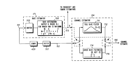
The operation of the presently preferred embodiment of rate
estimator i71 is further illustrated in FIGS. 9 through 11. FIG. 9 shows a
logical block diagram, and FIG. 10 a flow chart, of the preferred approach
for rate and channel estimation in the receiver of FIG. 4. The rate
estimator 171 receives the noisy, faded reference samples 151 from
demultiplexor 430 (which knows the despread sample positions with
sufficient accuracy for demultiplexing the reference samples from the
data samples) as they are extracted (steps 802-804). These reference
samples 151 are buffered in buffer 705 of rate estimator 171 until all
symbols of the frame have been received (e.g., 96 symbols at full rate);
the reference symbol stream to timing control 176, frequency offset
estimator 172 and channel estimator 154 are previously buffered (see,
e.g., buffer 707 following demultiplexor 430, thereby buffering the
unrotated demultiplexed reference samples until the appropriate
sequence family can be fed to rotaters 433, 434, 436 and 437) so as to
delay their processing until a rate estimate 173 is received. Since not all
"symbols" received will correspond to transmitted symbols (e.g., at less
than full rate only the envelope of the information-bearing power control
groups is keyed on, so the remaining information is noise), the rate
estimator 171 performs a quasi-coherent correlation of the received
reference symbol stream in rate determiner 706 (which, in the preferred
embodiment, is achieved by a properly programmed ASIC (application
specific integrated circuit) or DSP (digital signal processor)). A quasi-
coherent correlation is used since the channel is coherent for the
SUBSTITUTE SHEET (RULE 2V~
2176945
WO 96!10879 PCT/U595109774
-26-
duration of a power control group (i.e., at 100 km/hr and 900 MHz in a
Rayleigh fading channel the channel is coherent for under 4 ms). The
correlation is performed (step 812) against each of the possible transmit
sequences, for example the full, half, quarter and eighth rate sequences
discussed above. The sum of the squares of the partial inner product
(denoted Mi) is preferably used, scaled by a factor k;. M; may be
determined according to the following:
16 ~ 6
M; _ ~ ~ r~.rn. ~ * (eq. 7)
m ;=I
where r~ is a received reference symbol and s~,; is one of the possible
sequences denoted {sp}, {s~}, {s2}, {s3} for the full through eighth rates,
respectively. In each of the 16 power control groups there will be 6
reference symbols, so the coherent correlation is done over the time
span of each power control group. The partial correlation result is
squared for each group and the sum of the squares over the 16 groups is
determined. This is scaled by a factor k; = 1, 2, 4 or 8 for i = 0, 1, 2 or 3.
The index of the maximum of the scaled results is outputted as the rate
estimate 173, or R. In the alternative, the reference sequences could be
expanded to include other, e.g., power control, information from the
transmitting subscriber. For example, for transmission of full, half and
eighth rate, plus the 1 bit of power control information, 6 sequences {s;}, i
= 0,...,5 are used.
This method of rate estimation is much less complex, and more
accurate at full rate, than the proposed technique for IS-95 uplink
communications, which could have been applied to the IS-95-like radio
described herein. In the proposed IS-95 technique rate determination is
done by running a 256 state Viterbi decoder four times, once for each
possible rate. The parity check words (CRC, or cyclic redundancy check,
or other frame quality indicator) are then examined for each of the four
decoded streams to see which indicates the most likely (i.e., error-free)
rate. As a skilled artisan will appreciate, such a proposed approach is
computationally more intensive and less accurate than the solution of the
present-invention. Simulations show that an energy based rate detector
SUBSTITUTE SHEET (RULE 26)
2176945
~VO 96!10879 PC1'IUS95109774
_27_
or exhaustive decoder methods falsely identify a full rate frame as
subrate about 0.3 to 0.5% of the time, versus a falsing rate for the
reference symbol based rate detector of less than 0.1%.
Following a determination of the rate estimate 171, this is inputted
to each of the channel estimator 154, frequency offset estimator 172 and
timing control 176 (steps 814-818). The rate estimate 171 is used to
select the reference demodulating sequence (synch(I) and synch(Q) of
FIG. 4, equivalent to {sR} of block 171 of FIG. 9, also equivalent to aref(n)
of eq. 2), used in extractor 150 to rotate the demultiplexed reference
symbols from DEMUX 430. After the rate estimate becomes available
and the rotator inputs and channel estimator filter are selected, the rotator
and filter operation may be done concurrently. That is, as each rotator
sample becomes available, one channel estimation filter output is then
calculated. The rate estimate 171 is used to control the selection of a
filter to operate on the rotator outputs in the channel estimator 154.
Where the rate estimate is R = 0 (i.e., full rate), all symbols of the frame
are input to a full rate filter 711. This is further illustrated in FIG. 11 by
signal 905, showing only those reference symbols 905, from the signal
stream 902, that are within the frame period 906 being operated on by
the filter 711. The full rate filter output 712 is then outputted from the
channel estimator 154 as the channel estimate 156. When the rate
estimate is other than R = 0 (e.g., 1, 2 or 3) the reference symbols 152
are fed into filter 714, with the output 715 then serving as channel
estimate 156. The input to filter 714 (illustrated in FIG. 11 ) is limited to
those reference symbols 903 within the energized power control group
periods 904. While only two filters have been shown, a skilled artisan
will appreciate that a different filter (or algorithm) may be used for each
rate estimate 173. For instance, at half rate, some groupings of 2 and 3
consecutive energized power control groups will occur under
randomization. In that case, a good channel estimation filter will give
some nonzero weight to neighboring energized groups in producing a
channel estimate for a given group in the frame. It should also be
appreciated that the overall filtering function is nonlinear, since the
reference symbols themselves are determining the filter transfer function.
The channel estimator filters 711, 714 serve to construct a
SUBSTITUTE SHEET (RULE 2fi)
2176945
WO 96110879 PCTIUS95109774
_28_
channel estimate 156 from at least a portion of the received noisy, faded
reference symbol stream. The channel varies a great deal over the
duration of the frame, so the channel estimate is computed repeatedly; a
sequence of channel estimates emerges at 156. For instance, the
channel may be estimated such that there is an output once per power
control group segment of the received frame, that is, 16 estimates per
frame. These channel estimates are used by detector 160 to phase
align all of the received data symbols 158 to a 0 phase reference over
the span of the entire frame (step 820). In that way, they may be
efficiently combined with distorted copies of the same sequence from
other antennas or channel delays before being near-optimally decoded
in the Viterbi decoder 182. Just as the decoder 182 pertormance is
better if its input is coherent over the frame length, the channel estimation
filter 711 or 714 produces a better channel estimate if its input is
coherent over the entire span being considered. For example, consider
a received frame which is full rate, meaning information energy is present
in all 16 power control groups. The channel estimation filter 711 or 714
will reduce the noise in its output most (yielding the highest signal to
noise ratio estimate) if it operates on a time span, Tf, of noisy, faded
samples roughly equal to the channel coherence time, Tc. The channel
estimator 154 is in a sense an application of the idea of "smoothing," not
"filtering." The estimator 154 is estimating the channel at time to and
effectively has access to measurement data from t = -~ to t = +~. For the
conditions of 100 km/hr and 900 MHz, T~ is about 4 ms or 3 power control
groups (at 1.25 ms per power control group). T~ varies in an inverse
proportion to vehicle speed. The signal to noise ratio of the estimate will
be highest if Tf is about equal to Tc (the precise shape of the filter is
readily derived from Weiner filter theory, if the fading and noise process
statistics are known); the filter should operate over 3 power control
groups.
This latter point is significant. If the filter 711 or 714 is always
operated over 3 power control groups it will provide a very suboptimal
channel estimate on subrate data, since pure noise will be regularly
injected into the filter via the non-energized power control groups. The
aftemative under prior approaches, operating a filter designed for a
SUBSTITUTE SHEET (RULE 26~
2176945
~VO 96!10879 PCT/US95I09774
_29_
subrate, is suboptimal when it turns out that the received frame was full
rate (suboptimal because Tt«T~). The present invention solves this
problem by estimating the speech rate with high accuracy before the
channel estimate is done. This allows the appropriate filter 711 or 714
to be implemented for the current frame, yielding the best channel
estimate in the full rate case, and a good estimate in the subrate case. In
an alternative embodiment, where the number of filters is expanded,
each of the various subrate cases (e.g., half, quarter and eighth) are
optimally filtered.
Similar to the channel estimator 154, the rate estimate 173 is
used by timing control 176 to filter the energized power control groups
and by frequency offset estimator 172 to mask out the non-energized
groups (steps 814-816). Appropriately filtered, the timing control 176
computes the timing measure (i.e., difference) and adjusts the taps as
described above based on the energized groups (step 808). Step 806
illustrates an approach in which the energy estimate, computed using the
noisy reference bits, of the on-time branch may be computed once per
power control group and used to set or clear the downlink power control
bit (i.e., informing the mobile whether its power is too high or low). In
addition, the rate information may be used to indicate which slots are
unoccupied, for example as information to the Viterbi decoder 182 of
where the noisy samples are, for use by a signal to noise ratio estimator
in scaling the input to the decoder 182 during subrate frames.
FIGS. 12 and 13 illustrate some of the benefits obtained by use of
the rate estimate information. FIG. 12 illustrates the real outputs from
channel estimator 154, where the signal to noise ratio (SNR) of the input
signal 910 to filter is -0.5 dB. The subrate filter 714, in which Tf « T~,
yields a channel estimate 916 with calculated output SNR = 8.0 dB. On
the other hand, a full rate filter in which Tt =T~ yields an improved
channel estimate 914 with calculated SNR of 10.9 dB.
In the case of timing estimation, FIG. 13 illustrates how, if rate
information is available, timing error can be tracked very well during full
rate frames. Using the present invention, we use all 16 groups when all
16 are energized and only use 2 of the 16 when necessary (i.e., for
eighth rate). In Figure 13, the true channel timing 920 is simulated as
SUBSTITUTE SHEET (RULE 26j
a ' - 2176945
WO 96/10879 PCT/U595109774
-30-
stewing in a sinusoidal fashion, reaching peak values of one half chip
period off of a mean value of 0. The timing circuit tracking is shown by
the curare 924. The net error is shown by the third line 926. At between
and 10.2 seconds of elapsed time, the error is shown increasing to a
5 value of 0.2 chip periods. During this time, almost all frames received
were subrate, and timing updates were slow in coming. At about time
10.38 seconds, a burst of full rate frames began to be received. The rate
estimator 171 detected that the frames were now full rate and allowed
the timing circuit to operate on all received symbols. This led to rapid
10 and correct timing corrections, bringing the timing error back to
approximately 0.
Although the invention has been described and illustrated
with a certain degree of particularity, it is understood that
the present disclosure of embodiments has been made by way
of example only and that numerous changes in the arrangement
and combination of parts as welt as steps may be resorted to
by those skilled in the art without departing from the
invention as claimed. For example, the modulator, antennas
and demodulator portions of the preferred embodiment
communication system as described were directed to CDMA
spread-spectrum signals transmitted over a radio
communication channel. However, as will be understood by
those skilled in the art, the encoding and decoding techniques
described and claimed herein can also be adapted for use in
other types of transmission systems like those based on time
division multiple access (TDMA) and frequency division
multiple access (FDMA). In addition the communication
channel could alternatively be an electronic data bus, wireline,
optical fiber link, satellite link, or any other type of
communication channel. Thus, it will be apparent to one
skilled in the art that while the invention has been described ,
iri conjunction with specific embodiments thereof, it is
evident that many alterations, modifications, and variations
are possible in light of the foregoing description. Accordingly,
the invention is intended to embrace all such alterations,
SUBSTITUTE SHEET (RULE 26~
2176945
. WO 96/10879 PCT/U595/09774
-31-
modifications, and variations within the spirit and scope of
the appended claims.
SUBSTITUTE SHEET (RULE 21i~