Note: Descriptions are shown in the official language in which they were submitted.
2176ggg
A MEMORY CHIP ARCHITECTURE FOR DIGITAL STORAGE OF
PRE-RECORDED AUDIO DATA WHEREIN EACH OF THE MEMORY
CELLS ARE INDIVIDUALLY ADDRESSABLE
FIELD OF THE INVENTION
The present invention relates to an organization of components on a digital
recording medium, and more particularly to a unique semiconductor storage
medium for addressable storage and retrieval of reproducible pre-recorded
audio.
BACKGROUND OF THE INVENTION
A variety of recording media exist today for the storage of consumer directed
pre-recorded music and other audio applications. These media include CD ROM
(Compact Disc Read Only Memory ), DAT (Digital Audio Tape) and traditional
magnetic cassette audio tape, just to name a few. Of the above technologies,
the
compact disc format has steadily increased in popularity and gained consumer
approval due to the high sound quality of the digitally stored audio, as well
as ease
of use.
Compact discs and other formats, however, have some significant
disadvantages. For one, compact discs do not normally include the ability to
register the content of the information stored on disc prior to selection at a
player.
In other words, in order to gain any information regarding the contents of a
particular music selection, that selection will first have to be in some
manner
manually accessed at the player. In the alternative, some CD players may be
;.::~,
2I 76988
2
manually programmed to play certain selections based upon user input. In
either
circumstance, however, there is no way to automatically search and play music
by
category, for example, by artist, music type, etc., unless a user has prior
knowledge
with regard to the selection.
In addition, compact discs, or optical digital discs, as they are sometimes
referred, require mechanical drive systems of high accuracy and precise servo-
controllers to be used in conjunction with solid state lasers for operation of
a CD
player. Thus, the fact that the disc must be rotated at a constant linear
velocity
during play requires a substantial number of precision-made movable mechanical
to parts which tend to fall out of design tolerance due to wear. This and
other factors
tend to limit the ruggedness and portability of present day CD systems.
Moreover,
because of the size of CDs and the need to protect their playing surfaces, the
ability
to conveniently transport more than a few compact discs at one time is also a
limiting factor.
SUMMARY OF THE INVENTION
The present invention is directed to a memory device for digital storage of
pre-recorded audio and other digitally stored data relating thereto. The
memory
2o device includes components for addressing, retrieving and automatically
searching
the stored data. In an illustrative embodiment, an array of memory cells for
storage
__ ~ 217698a
3
of the digitally recorded audio is contained within a modestly sized plastic
package.
In the preferred embodiment, the memory cells are comprised of Read Only
Memory (ROM). Each of the memory cells is individually addressable over a
parallel address bus and data is read and/or written over a parallel data bus.
Data is
transmitted to and from the device by means of a serial interface with a solid
state
audio player. Shift registers within the memory device are coupled to the
serial
interface for transmitting serial data to and receiving serial data from the
audio
player. Data buffers are interposed between the address bus, data bus and
respective shift registers for storing data to be placed on the address bus
and
receiving data from the data bus. In accordance with one aspect of the
invention, a
series of capacitive plates is included to provide a contact-less interface
between the
memory device and the associated solid state audio player.
In accordance with one aspect of the present invention there is provided a
memory chip for storage of digital data, said digital data corresponding to
pre-
recorded audio and said memory chip adapted for insertion into an associated
audio
player, said memory chip comprising: a plurality of memory cells, each one of
said
memory cells being individually addressable for accessing of data therefrom;
first
means coupled to said plurality of memory cells for receiving serial input
data from
said associated audio player; and second means coupled to said plurality of
memory
cells for outputting serial data from said memory chip; said memory chip being
adapted to receive a do power, ground and clock signal from a do offset
circuit in
said audio player, wherein said do power and clock signal are transferred in
combination with one another over a single contact; said do offset circuit
including
a do offset generator having a transistor biased by a resistive divider
network for
2176988
3a
producing said do power signal, a diode-resistive network for passing through
said
do power signal and preventing bleed-back of said clock signal and a mixing
means
for mixing said clock signal with said do power signal, wherein said do offset
circuit provides a buffer between said do offset generator and an exposed
contact;
and said memory chip including a recovery circuit, said recovery circuit
having a
low pass filter for recovering said do power signal, and a do current blocking
means
coupled to a transistor amplifier for recovering said clock signal.
In accordance with another aspect of the present invention there is provided
a semiconductor chip memory apparatus for storage of pre-recorded audio, said
memory apparatus adapted for use with a solid state audio player, said
apparatus
comprising: a plurality of memory cells for storing digital data therein;
address
shift register for receiving serial data corresponding to addresses of memory
locations; data shift register for outputting serial data read from selected
memory
locations; said chip memory including a housing, said housing including a
graphics
display area for inclusion of indicia pertaining to said pre-recorded music;
and said
housing including a hole disposed at an end thereof, whereby said apparatus
may be
transported by means of a carrying device attached through said hole.
BRIEF DESCRIPTION OF THE FIGURES
For a better understanding of the present invention, reference may be had to
the following description of exemplary embodiments thereof, considered in
conjunction with the accompanying drawings, in which:
FIG. 1 A shows a perspective view of one preferred embodiment for
the packaging of the present invention memory chip;
2176988
4
FIG. 1 B shows a plan view for an underneath portion of the present
invention memory chip;
FIG. 2 shows one preferred embodiment of the internal circuitry for the
present invention memory chip;
FIG. 3 shows one preferred embodiment for an interface used with the
present invention memory; and
FIG. 4 shows one preferred embodiment of a do offset circuit in the
audio player used for mixing in the clock signal and a recovery circuit in the
music
chip used to recover each of the signals.
to
DETAILED DESCRIPTION OF THE DRAWINGS
Referring to FIG. lA, there is shown one preferred embodiment of an
integrated circuit package for the present invention memory chip, hereinafter
referred to as a music chip 10. The music chip 10 is essentially a memory
component which is adapted to be received into an accompanying solid state
audio
player for playing music contained in memory. The physical characteristics of
the
chip 10 are essentially that of a flat rectangular device having dimensions of
approximately 2.5" x 1.125" x 0.25" and housed in a rugged ABS plastic
(acrylic
butyl styrene) or other like material. The relatively modest sized music chip
device
will have significant advantages over compact discs and other media with
regard to
2176988
transportability and storage. Memory and interface circuitry of the chip 10
are
embedded within the package, as will be explained.
The music chip 10, as will be understood is intended for the storage of pre-
recorded audio, namely, music. A graphics window 12 is included on a top
surface
5 14 of the chip for display of artwork and other indicia associated with pre-
recorded
music sold in retail markets. Thus, the graphics window 12 will contain
information
similar in scope to that found on the front of a compact disc or cassette tape
package. A front portion of the chip 10, at an opposite end from the graphics
window 12 includes a cylindrical hollow 16 extending completely through the
flat
body portion of the chip. The hollow 16 presents a convenient manner for
carrying
one or more of the chips, in that the devices may be strung through the hollow
and
retained on a key chain or in another similar manner. On either side of the
chip 10,
proximate the graphics window 12, metal contacts 18, 19 are positioned for
supplying power, ground and clock signals to the circuitry of the chip. A 45
degree
notch 20 is located in the top right hand corner of the chip 10 in order to
conveniently designate the back end 22 of the chip as an area which should be
first
inserted into the audio player. The notch 20 also distinguishes face-up versus
face-
down insertion of the chip 10.
Referring to FIG. 1 B, an underside view of the chip 10 is depicted. A set of
four capacitive plates 23-26 are embedded in the underside 28 of the chip for
transfer of data between the chip and player. Utilizing the embedded
capacitive
2I 7698
6
plates 23-26 in conjunction with the rugged plastic housing material makes the
device extremely tolerant to most any type of handling. In addition, because
of the
unique packaging and associated circuit design, many problems common to other
types of integrated circuits, such as electro-static discharge (ESD), are
greatly
minimized.
The memory of the music chip 10, as has been explained, will contain
prerecorded music or other like audio content, wherein the music is stored in
a
compressed digital format. Compression is performed according to an audio
coding
algorithm, a detailed discussion of which is not required for understanding of
the
present invention.
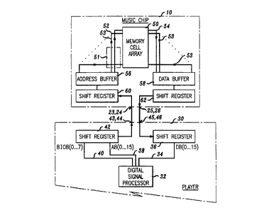
Referring to FIG. 2, there is shown one preferred representation for the
internal circuit configuration of the present invention music chip 10. As has
been
mentioned, the music chip, 10 is adapted to be received into a solid state
audio
player. FIG. 2 depicts the music chip 10 as it is coupled to such an audio
player 30.
It will be understood that the audio player 30 will be any one of a number of
devices, for example portable or stationary, which devices are adapted to
access,
receive and play digital audio stored in memory of a music chip 10. As shown,
the
audio player 30 includes a digital signal processor (DSP) 32 for decoding the
digitally stored data in memory of the music chip. A data line 34 is coupled
from
2o the DSP 32 to a data shift register 36 on the player 30. An address line 38
and bit
I/O line 40 are similarly coupled from the DSP to an address shift register
42. The
2176988
address, bit I/O and data lines send and receive data to and from the shift
registers
36, 42 which in turn send and receive data to and from the music chip 10. It
will be
understood that the address, bit I/O and data lines may be in bus format to
accommodate parallel data transfer. In this case, the shift registers 36, 42
would
necessarily be adapted to receive the parallel data and then output same in
serial
form, or in the alternative, receive serial data and be able to output the
data in
parallel. In either case, data is then transferred serially to and from the
shift registers
36, 42 of the audio player 30 via matching capacitive plates 43-46 which
correspond
to the capacitive plates 23-46 of the music chip 10. The corresponding plates
come
l0 into alignment when the music chip 10 is inserted within the audio player
30
creating a plurality of capacitors which form a capacitively coupled
interface.
Referring again to FIG. 2, it can be seen that the structure of internal
memory 50 the music chip 10 appears similar in nature to that, for example, of
a
flash EEPROM. An array of memory cells 50 is included therein, wherein each
memory cell 50 is individually addressable via a parallel address bus 52. Each
memory cell 50 is read from (or written to, if applicable) over a parallel
data bus 54.
The memory for the music chip will typically be Read Only Memory (ROM),
wherein the pre-recorded digital audio will be represented in a mask which is
copied
at time of fabrication and which will exactly replicate the audio of a master
2o encoding from which it was reproduced.
2176988
As an alternative, the memory of the music chip can also be a type of
programmable ROM (PROM), wherein each of the memory cells is written to a
single time in order to store blocks of audio. As another alternative, the
memory
could also be a nonvolatile Random Access Memory (RAM) device, for example,
FLASH RAM, wherein both read and write operations may be accomplished. In the
case of pre-recorded audio, however, write operations to the music chip will
never
normally be necessary once the audio has been recorded, thus, the additional
production costs associated with RAMs would not appear justified.
Within the shown embodiment of the music chip 10 in FIG. 2, a parallel
address bus 52 and data bus 54 are coupled to each of the memory cells 50. It
will
be understood, of course, that the address bus may be coupled to the memory
through decoder circuitry 51, which is known in the art. As shown, the address
bus
52 and the data bus 54 are uni-directional buses with the designated arrows 53
being
representative of the direction of data flow. That is, addresses from the
audio player
are accepted into the music chip to access specific memory locations, while
data
from the memory cells, after being accessed, is then output over the data bus
54. It
will be understood, however, that the data bus, in particular, may be made to
be bi-
directional depending on the memory technology employed within the chip.
As can be seen in FIG. 2, the address bus 52 is coupled to an address buffer
56 and in a similar fashion the data bus 54 is coupled to a data buffer 58.
The
address buffer 56 and data buffer 58 are in turn coupled to an associated
address
2~~s9ss
shift register 60 and data shift register 62, respectively, in the music chip
10. The
function of the address buffer 56 is to receive from the address shift
register 60,
wherein the address data can be accessed in parallel form, and output these
addresses over the parallel address bus 52. In reverse fashion the data buffer
56
receives parallel data from the data bus 54 and temporarily buffers the data
for
parallel loading into the data shift register 62. Addresses and data are
transferred
serially to and from the shift registers 60, 62 of the music chip by means of
the
capacitive plates 23-26 which are aligned with the capacitive plates 43-46 of
the
audio player 30.
1o The transfer of addressing information and data to and from the chip 10 to
the audio player 30 by means of capacitive plates 23-26 provides a significant
advantage over other memory chip packages since the need for exposed
electrical
contacts is avoided. Conductive plates or electrodes having outer dielectric
surfaces
on both the chip 10 and the audio player 30 form an electrical interface when
each
plate in the chip is aligned in close proximity with a corresponding plate in
the
player. When the chip 10 is in place within the audio player, addressing
information
and data are then reliably transferred. This remains true even after some time
of use,
since as for the data transfer circuitry, there are no exposed metal surfaces
to corrode
or to which particles may collect. In addition, the potential of damage from
electrostatic discharge to electronics within the chip is minimized since an
insulator
in the form of a dielectric is provided between the conductors of the chip and
any
10
2176988
sources from which the discharge might occur. It will be understood that other
types
of interfaces may also be utilized, for example metallic contacts, however,
the
capacitive interface is preferred for the reasons discussed.
Referring to FIG. 3, there is shown a more detailed illustration of the
capacitive interface found within the music chip 10 and audio player 30.
Capacitive
plates 23, 24 are coupled to an address data receive circuit comprised of a
differential
amplifier 70 adapted to receive data from corresponding capacitive plates 43,
44, the
corresponding capacitive plates 43, 44 being coupled to differential drive
circuits 80
on the player 30. The output of the differential amplifier 70 is coupled to
the input
of the shift register 60 which receives the serial addressing information as
explained
with reference to FIG. 2. A data output drive circuit, comprising driver
amplifiers
72, 74, is coupled to the data shift register 62 and receives serial data
therefrom to
differentially drive the capacitive plates 25, 26. The capacitive plates 25,
26 coupled
to the drive circuit are then capacitively coupled to corresponding plates 45,
46 in
the player when the chip is inserted, wherein data is received at a
differential
amplifier 81 and received at shift register 36. The driver amplifiers 72, 74
convert
serial data from the data shift register 62 of the music chip which is of one
polarity,
into a differential polarity such that for each transition of a signal from
the chip, one
of the drivers goes positive, while the other goes negative. Thus, two of the
2o capacitive plates on the chip are utilized for data (or addressing) input,
while two
plates are used for data output. As can be seen, a minor image of the same
scheme
i -x:
2176988
is used for the player 30. The differential data transfer scheme ensures a
more
reliable transfer of information since two data terminals are active to
indicate a
transition from one state to another. Moreover, hysterisis is built into the
data
receive circuits to prevent false triggering from outside noise.
As has been explained, metallic contacts 18, 19, made for example, from
nickel clad copper, are located on either side of the chip 10 to provide
power,
ground and clock signals to the internal circuitry thereof. Although metal
contacts
18, 19 are provided on the chip, the contacts are mounted closely to the body
of the
chip so as not to protrude a great distance therefrom. This, in combination
with
to surge protection coupled to the circuit lines running from the contacts
will reduce
the possibility of damage from ESD.
In a preferred embodiment of the invention, only two contacts are used to
provide power (3.3 VDC), ground and clock signals, wherein the clock signal is
transmitted in conjunction with one of the power connections. This is done to
reduce susceptibility to ESD by minimizing the exposed contact area, as well
as to
minimize the effects of corrosion on exposed metal surfaces. Referring to FIG.
4,
there are shown preferred embodiments of a do offset circuit 90 and clock
recovery
circuit 92 used in the audio player 30 and music chip 10, respectively, to
transmit
the power and clock signals together from one contact. The do offset circuit
90
includes transistor T1 (MOSFET) which is biased by means of resistive divider
network comprised of resistors R1 and R2 and functions to provide a stable do
offset
_. 12
z~~s9ee
for the voltage output VDD of the audio player 30 . The offset signal from the
transistor T1 enters a diode-resistive network 91 which prevents bleed-back of
the
clock signal (OSC) into the power circuit. Diode D1 is forward biased to pass
the
offset signal. R3 is assigned a relatively large value, for example, one mega-
ohm,
so as to be able to pass only minimal feedback current. The clock signal (OSC)
is
added or mixed with the do offset signal at junction J1 where the clock signal
effectively rides on the do carrier, as shown. Besides providing a stable
offset value,
the do offset circuit of FIG. 4 also creates a buffer between the power
circuitry and
the exposed contact. The values of R 1 and R2 are chosen according to the
desired
to offset, wherein typically, R1 is selected to be much greater than R2.
The combination signal is transferred from the audio player 30 to the music
chip through one of the metal contacts 18, 19, wherein the clock is extracted
from
the power signal by means of a clock/dc voltage (VDC) recovery circuit 92. The
VDC recovery circuit is comprised of a low pass filter 94 including R11, CI 1.
R11
and C 1 I integrate the input signal over time to produce a do signal, wherein
VDC
appears at the output terminal 95 of the low pass filter 94. The clock
recovery
circuit 92 includes amplifying transistor T2 which is driven into enhancement
or
depletion mode by the ac clock signal. Capacitor C21 blocks the do portion of
the
combination signal and the extracted clock signal appears at an output
terminal 97
2o which is coupled to the drain of transistor T2. Depending on the clock
frequency
utilized, R11, C11 and RD, RS are chosen so that RD is much greater than RS.
It
2176988
13
will be understood that in the alternative, three contacts may be provided for
the
transfer of each of the signals individually. As is known in the art, data
transfer is
coordinated throughout the music chip 10 and audio player by means of the
clock
and other corresponding signals which are issued from the DSP.
In operation the present invention music chip 10 functions as follows. An
address request is issued from the DSP 32 of the audio player 30 to read the
contents
of the data in a specific memory location of the music chip. Addressing
information is transferred to the address shift register 42 of the audio
player wherein
it is transferred over the capacitive interface plates of the audio player and
the chip,
to respectively. The address is received at the data receive circuit of the
music chip 10
where it is converted to a standard serial data string and then stored in the
address
shift register 60. In accordance with the clock cycles and control signals of
the DSP
32, the address information from the address shift register 60 is gated into
the
address buffer 56 where the information is placed on the parallel address bus
54 to
access a specific memory location. Once the specific memory cell has been
identified, data is read from the memory cell and placed on the parallel data
bus 54.
The data is transferred over the data bus 54 and received in parallel at the
data buffer
58 . Data from the data buffer 58 is then loaded into the data shift register
62 in
parallel form. The data loaded in the data shift register 62 can then be
serially
2o output through the driver circuitry over the capacitive interface where it
is received
at the data shift register 36 of the audio player 30. The data is then ready
to be
processed by means of the DSP 32. In a preferred embodiment of the invention,
data transfer to and from the memory will take place at a 150 Khz rate.
A unique architecture for digitally storing audio within a semiconductor chip
has thus been presented. The chip allows for serial transfer of data to and
from the
21'6988
14
chip by means of a capacitively coupled interface to the audio player. Serial
data is
then converted and transferred within the chip by means of parallel address
and data
buses. Data is then once again output in a serial fashion for decoding and
processing by the audio player.
From the above, it should be understood that the embodiments described, in
regard to the drawings, are merely exemplary and that a person skilled in the
art may
make variations and modifications to the shown embodiments without departing
from
the spirit and scope of the invention. All such variations and modifications
are
intended to be included within the scope of the invention as defined in the
appended
I0 claims.