Note: Descriptions are shown in the official language in which they were submitted.
~ 77052
--1--
CIIARGE PLATE FABRICATIQN PROCESS
Technical Field : ::
The present invention relates to binary
continuous ink jet printers and, more particularly,
to improved construction for the charge plate in
such printers.
Backaround Art
In continuous ink jet printing,
electrically conductive ink is supplied under
pressure to a manifold region that distributes the
ink to a plurality of orifices, typically arranged
in a linear array(s). The ink discharges from the
orifices in filaments which break into droplet
streams. Individual droplet streams are selectively
charged to substantially two levels in the region of
the break off from the filaments and charged drops
are deflected from their normal trajectories.
Either the deflected drops or the undeflected drops
are caught and recirculated, and the other drops are
allowed to proceed to a print medium.
In binary continuous ink jet, ink drops
are charged by a charge plate having a plurality of
charging electrodes along one edge, and a
corresponding plurality of connecting leads along
one surface. The edge of the charge plate having
the charging electrode~ is placed in close proximity
to the break off point of the ink jet filaments, and
charge is applied to the leads to induce charges in
the drops as they break of f f rom the f ilament~ .
In U.S. Patent No. 4,560,991, issued
December 24, 1985, to W. Schutrum, one method of
fabricating a charge plate is described. The charge
plate taught by Schutrum is fabricated by electro~
depositing the charging electrode~ and leads on a
~ ~ Z177052
-- 2 --
flat sheet of etchable material, such as copper
foil, to form a so-~called "coupon. " The coupon is
bent in a jig at approximately a 90angle. The
leads are then bonded to a dielectric material, such
as aluminum oxide, and then the etchable substrate
is removed by chemical etching. Such a charge plate
fabrication method is a "lead transfer" method, in
which the formation of electrodes on an etchable
substrate is required.
Another "lead transfer" charge plate
fabrication method is described in commonly assigned
application Serial No. 08/229,114, which also
requires the formation of electrodes on an etchable
substrate. This electroformed coupon is then bent
15 at approximately 90 degrees, bonded to a dielectric
material, such as aluminum oxide, and then the
etchable substrate is removed by chemical etching.
Unfortunately, several problems exist
with prior art charge plate fabrication techniques,
20 such as the complexity of fabrication stemming from
the relatively large number of manufacturing steps
required to make a usable charge plate, as well as
the cost associated with these manufacturing steps.
There is also a loss of precision related to the
25 lead transfer process, as the leads tend to move
slightly when the substrate is etched away. As the
spatial distance between jets is decreased, there is
an increasing proolem with connectiong to l-~t~n~l
circuitry. For example, standard electronic
30 connection technology can make approximately 20
electrical connections per linear inch of connector.
More exotic technology can make reliable connections
at 100 connections per inch. It is desired to have
several hundred charge leads per inch in a modern
ink jet printer. Currently, this is accomplished by
77~2
--3 --
"fanning out~ the leads from the front edge of the
charge plate to a longer connection area in the part
of the charge plate away from the ink jet process.
For example, a one inch wide printhead with 300 je~s
per inch requires at leaE3t three inches of connector
space which must be provided at the rear Df the
charge plate. It is seen that this results in a
charge plate and an ink jet printhead which i~ much
larger than the desired small size. Another problem
with the current charge plate fabrication technology
relates to condensation on the charge plate during
the operation of the printhead. Since the charge --
plate operates in a 1009~ relative humidity
environment, water tends to condense on the charge
plate. To avoid this problem, a heater as taught in
U. S . Patent No. 4, 622, 562 is employed to keep the
charge plate slightly warmer than the surrounding
environment. In the present art as taught in the
Schutrum patent, 4, 660, 991, the catcher heater is an
2 0 added component under the charge plate in the
catcher. Fabrication of this added component into
the printhead adds cost and complexity to the
printhead. Finally, nickel is commonly used as the
electroformed electrodes and as such, it i8 highly
vulnerable to electrochemical etching during the
operation of ~ the printhead during the ink j et
printing process. This is especially true of the
bottom portion of the lead~, those furthest from the
goo bend where ink tends to ~rrllmllli~te during the ==
ink jet printing process.
It is seen then that there exists a need
for an improved charge plate fabrication which
overcomes the problems associated with the prior
art .
~177052
--4 --
SummarY of the Invention
This need i8 met by the integrated
charge plate and electronic driver fabrication
process according to the present invention, wherein
5the charge plate fabrication technique allows for
fabrication by conventional methods, such as thin
film and thick film patterning, and integration of
the driver electronics onto the charge plate. Past
efforts to utilize these methods failed for several
10reasons First, electronic driver chips which could
withstand the high voltages required for the ink jet
process were not available Second, processe~ to
make the circuitry required on the charge plate were
not available at the spatial resolution required.
15Finally, the techniques required for making a chaEge --
lead which extended around a 90angle were not
available due to the inability to pattern over an
edge. Although a chip-on-charge plate could be
fabricated using the lead transfer method, this
20approach ha3 limitation~
The present invention oveEcomes previous
failures because in the subject method the
patterning of the top and the edge are separated,
which allows for more flex1bility in manufacturing.
25A clever combination of new technologies allows
fabrication of circuitry on the rear of the charge
plate 80 that electronic chip~ to drive the charge
leads can be mounted on the charge plate. Thi~
allows input to the charge plate over an electronic
30"bus" 80 that many charge leads can be driven from a ~ =
few interconnections to external circuitry. The new
technologies also allow inte~[ration of the charge
plate heater onto the bottom of the charge plate
In addition, material~3 which are available for
35fabrication with the new techniques have a lower
" ~ ~17~1~52
electrochemical etch rate.
In accordance with one aspect of the
present invention, a method of fabricating a charge
plate for an ink jet printer allows for fabrication
by conventional methods. Initially, a ceramic ~:
charge plate ~;ubstrate is provided, the substrate
having an edge, a bottom and a top. The substrate
is then edge printed to define a charging face on
the edge of the ceramic charge plate substrate. The
conductive path from the charging face to the top of
the ceramic charge plate substrate is completed by
top printing on the top surface to define a wrap
around circuit. Part of the top circuit is
patterning for the site on which the driver
electronic chips will reside. In this case, the
pattern consists of a number of small rectangular
conducting areas or "pads" which surround the driver
chip. The pads provide points to which connections
can be made from the charge plate to the driver chip
u8ing suitable technique8 which are known in the
art, such as conventional wire bonding techniques,
including gold wire ball bonding; flip chip
att~ t; ball grid array attachment, including
micro ball grid array att~ nt; and tape automated
bonding. Connections from the pads to the charging
face and to the rear of the chip are also fabricated
in this top patterning step. This patterning can be =~
accomplished by any suitable method such as by a
thick film process.: The charge plate can be top
3 0 patterned ta connect top electrical connections to
the f ront edge f or charging and def lecting . When
the conductive paths on the top of the ceramic
charge plate substrate are completed, a second set
of processes are used to form a region for two layer
35 circuitry at the rear of the charge plate For
21~7~2
--6 --
example, there is a need for an electrical grounding
beneath the electrical traces bringing power and
logic signals into the driver chips. Via holes
through the charge plate are also fabricated ~o that
thick film circuit technology can be used to create
a resistive charge plate heater on the bottom of the
charge plate.
Accordingly, it is an object of the
present invention to provide a charge plate wherein
inclusion of driver chips reduces the size of the
interconnect . It i~ also an obj ect of the present
invention to provide a charge plate wherein
fabrication by conventional methods, such as thick
film and thin film patterning, i8 allowed. It is a -
further object of the present invention to provide
such a charqe plate fabrication method which
overcomes previous attempts at similar fabrication
by separating the patterning of the toF and the ==~
edge, or front face, of the charge plate. It is a
further object to use thick ilm circuit technology
to create a connection for a 13tandard connector on
the back edge of the charge plate, to provide
circuitry required or electrical isolation of the
drive chip. It is a further object to integrate a
resistive charge plate heater onto the bottom of the
charge plate. Finally, it is an object of the ~ =~
present invention to allow for more flexibility in
manuf acturing .
Other obj ects and advantages of the
invention will be apparent from the following
description, the accompanying drawings and the
appended claims.
E~rief Descri~tion of the Drawinqs
Fig. 1 is a per~pective v ew of a charge
` 2177~2
-7--
plate substrate;
Fig. 2 i8 a perspective view of a
ceramic substrate, edge printed in accordance with
the present invention;
Fig. 3 is a perspective view
illustrating a wrap around conductive path on the
edge printed substrate of Fig. 2;
Fig. 4 is a perspective view
illustrating top patterning of the view in Fig. 3;
Fig. 5 is an exploded view illustrating
the layers of the charge plate fabricated in
accordance with the present invention; and
Fig. 6 is a block diagram illustrating
the power, ground, control and data interfaces to ---:
the charge plate of Fig. 1.
Detailed Descril~tion of the Preferred Embodiments
Referring to the drawings, a charge
plate substrate 10 of Fig. 1, capable of being
assembled into a charge plate assembly, is
illustrated. The charge plate substrate lo is
preferably ceramic and fabricated from 96~6 aluminum
oxide having a coef f icient of thermal expansion
(CTE) of 8 . 2x10⁻⁶/oc. A front edge 12 is
substantially perpendicular with a top surface 14.
The front surface is preferably flat to provide
optimum charge.
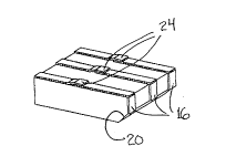
Referring now to Fig. 2, initially the
ceramic substrate 10 of Fig. l is edge printed on
its front edge 12 to define charge surfaces or
charging face 16. In a preferred embodiment of the
present invention, the height of the front edge 12
i8 approxlmately o . 015 inches . The front edge 12 is
substantially perpendicular to bottom surface 18.
Chamfer 20 separates the front edge 12 and the
-` 2177û52
--8 --
bottom surface 18 with an approximately 45 surface,
to provide clearance for drops deflected to the
catcher .
In a preferred embodiment of the present
invention, during edge print a small amount of ink
can be purposely allowed to extend over to the top
surface for improved electrical connection. The
charge surfaces 16 are defined by passing thick film
conductive ink through an opening in a screen, i . e .,
silk screen printing, and/or thin metal foil, i . e .,
stencil printing, using 8tandard processes in the
thick film processing art. Silk screening has the =~
advantage of allowing for the creation of unusual
patterns; while stenciling has the advantage of
providing improved quality of printed lines and
spaces without the wire mesh which can create
problems when pushing ink through at high
resolutions. A gold thick film paste, such as
commercially available DuPont 5715 Gold Thick Film
Paste, is preferable over nickel because gold is
more chemically inert than nickel.
Referring now to Fir. 3, subsequent to
defining the charge surfaces 16, a conductive path
is crn~;n~ to top surface 14, to create a wrap
around conductive path 22. During wrap around, in a
preferred embodiment of the present invention, these
lines can be permitted to extend over the front
edge. This creates an overlap from both the edge
and the wrap around print that ensures good
electrical cnnnrr~;r,n around the edge.
The wrap around 22 is also defined by
thick film paste or printing techniques, such as
printing, drying and firing steps. Hence, the
present invention applies thick film processing to
make the electrical connection between the top
` ~1770S2
g
surface 14 and the charging face 16. Electrical
connection from top surface 14 to the front surace -~-
12 is achieved using the electrical connection wrap
around process, which connects the front face
electrical connections 16 to top electrical
connections 22. This involves direct metal to metal
diffusion during the step of firing, prior to the
step of top patterning, and following the steps of
printing and drying, of the substrate.
Referring now to Fig. 4, top patterning
24 of the substrate is illustrated, subsequent to =-
the steps of printing, drying, firing, and metal to
metal diffusion, to create a charge plate. Top
patterning of the substrate can be by any suitable
means, such as use of Fodel photoimageable materials
as described in Proceedings of the 1993
International Symposium On Microelectronics
incorporated herein by reference. Fodel technology
is an extension of thick f ilm paste technology,
developed by cornbining inorganic components, metal
powders, glass powders, metal oxides and refractory
powders, used to make thick film dielectrics and
conductors with the organic components, polymers,
photoinitiators, ~ D and stabilizers, used to
make photoresist films for the printed wiring board
industry. This combination results in
photoimageable ceramic material that combines the
well known reliability of ceramic materials with the
ease of processing in conventional equipment, using
mild aqueous chemistries, currently used in the
printed wiring board industry.
The Fodel process, like the component
materials, is a combination of the conventional
thick film and printed wiring board~ processes. As
will be obvious to those sl-illed in the art,
~ 7~052
conv~ont;~,n~1 thick or thin film proces8es and
convention printed circuit board processes can be
used independently or in any suitable combination to
achieve the patterning of the charge plate of the
present invention. The Fodel process is described
herein for purposes of example only, and is not to
be considered as limiting the invention.
The Fodel process begins with the
application of a photoactive paste, such as a
commercially available Fodel paste, to the desired
substrate by blank screen printing. The paste is
allowed to level at room temperature and is then
dried, for example at a temperature of 80C. ~ After
drying, the paste is exposed in W light (with a
typical maximum wavelength of approximately 360 nm)
through the appropriate photomask to form a latent
image. Following exposure, the latent image in the
materials is developed such as in a conveyorized,
spray processor, for example using 1~ aqueous Na2C03 _-
solution. The developed paste is then fired by
conventional thick f ilm methods .
After the top patterning process
illustrated in Fig. 4, the top patterned surface is
coated with a material that has a high breakdown
voltage and is pinhole free. A preferred material
is a dielectric material which sinters to the top
patterned surf ace to make a good dielectric coating .
The dielectric coating may be any suitable
dielectric such as commercially available DuPont
5704 Dielectric.
A8 is well known in the art, thick ~ilm
technology is a method for producing patterned
circuity used in the electronics industry. The
pattern i8 silkscreened onto a substrate, then dried
and fired. The procese starts with a suitable
~ 7~2
substrate that can withstand the temperatures that
are necessary to sinter or "fire" the inks, such as
a substrate comprising 969i aluminum oxide. Thick
f ilm inks are then silkscreened onto the substrate .
Of course, various inks are ~available for different
applications. For example, certain conductive inks
can be used to form conductive gold traces; a
conductive ink that contains palladium-gold can be
used as solderable points; a more resistive type of
ink could be used to form re~iE3tive elements for an
electronic circuit or perhaps a resistive type
heater; a non-conductive or dielectric ink can be
printed to provide a protective coating over a
previously formed circuit or a barrier between two
circuit layers. These inks mainly consist of three
primary elements, including a binder constituent
(referred to as frit), a print vehicle and a
functional constituent. Once the ink is
silkscreened onto the substrate it is sent through a
drying furnace where the temperature reaches
approximately, for example, 150C, for the purpose
of evaporating all solvents. The next step is to
f ire the printed and dried substrate . The part is
subjected to a specific temperature profile where
the part is raised to and dwells at a temperature
where all organic matter i~ burned off, for example,
500C. The part is then subjected to a temperature
where firing actually takes place, 13uch as 850C.
At 850C the functional constituent is sintered into
a layer of functional material. Likewise, the frit
sinters and partially diffuses into the substrate,
thus providing a means to adhere the functional
constituent to the substrate. Finally, the
temperature is lowered. Additional layers can be
placed on top of each other and would follow the
- 217~2
-12 -
same process.
Referring now to Fig. 5, ceramic
substrate layer 26 is edge printed with edge print
layer 28, such as a gold thick film. A wrap around
layer 30 is then applied, which may be any suitable
material such as gold thick film. A fine line
circuity layer 32 is formed using the Fodel process.
This layer provides a connecting path between charge
driver chips 34 and charge electrodes on edge print
28. A ground plane circuity 36 is then applied to
provide an electrical ground path between the
connector 38 and the driver chips 34. These two
separate layers are then coated with a dielectric
layer 40 which sinters to the top of the patterned
surface8 and makes a good electrically insulated
coating. The control circuity layer 42 provides a
path for po~er, control and data signals between the
connector 38 and the driver chips 34.
Ref erring now to Fig . 6, there is
illustrated a block diagram showing the functional
r~l~t;nn~hips between the various layers on the
charge plate and connection to supporting
electronics remote from the oharge plate. In Fig.
6, power, control and data lines 44, 46, 48,
respe~ctively, are connected to power supplies 50,
print controller 52 and print data generator 54,
respectively, through the connector 38.
Ref erring back to Fig . 5, a second
dielectric coating 56 is applied to protect the
control circuity as well as to provide a second
coating over the fine line circuity 32. It is
important that the dielectric coating be free of
voids in the area of the f ine line circuitry .
Otherwise, conductive ink used in the ink-]et
printing process could provide a conductive path
` 2~ 77~2
-13--
between two adjacent traces and cause an electrical
short which could lead to component failure.
Continuing with Figs. 5 and 6, the
driver chips 34 are silicon devices that accept
logic level data in a serial fashion, then latch
those signals and output the same data in parallel,
but with much higher voltage potential. Logic
levels are typically 0 and 12 volts dc. The output
voltages can range from 60 to 180 volts dc. The
input channels of the driver chips 34 are connected
to the ground plane 36 and the control circuity 42
by suitable mean8 such as gold wire ball bonding.
The output rh~nn ~l ~ of the driver chips 34 are
connected to the fine line circuity 32, also by
suitable means such as gold wire ball bonding. An
epoxy or other suitable material is used to cover
the chips and the wire bonds, to protect the chips
and wire bonds from the environment.
Continuing with Figs. 5 and 6, connector -~
38 is applied through standard surface mount
soldering techniques. A solderable metal layer
provides pads where ~the connector is soldered on,
and small holes in the back are plated through to
create conductive vias from the top surface to the
bottom surface. This provides an electrical path
from the top to the bottom of the charge plate, and
to a resistive charge plate heater. The resistive
charge plate heater, comprised of resistive layer 58
and heater circuit layer 60, is integrated onto the ==
bottom surface also using thick film technology.
The heater circuit 60 is applied using the
solderable ink and provide, the conductive path
between the vias and the heater layer 58. The
heater layer 58 is then applied using resistive
inks. The shape and thickness of this layer
L770~
-14 -
determines the resistance desired.
The top patterned fine line circuitry
layer 32 provides the conductive path between the
wrap around pattern and the output of the driver
chip. This layer includes pads used in the wire
bonding operation. Ground plane circuitry layer 36 ~ ~
provides a ~nn~ ive path for the ground signals
between the driver chips and a surface mount
connector. The top patterned surface is coated with
dielectric layer 40 which sinters to the top
patterned surface to make a good dielectric coating.
Control circuitry layer 42 provides a conductive
path between the connector and driver chips before
second dielectric layer 56 is applied. Charge
driver components indicated as layer 34 and surface
mounted connector 38 provide a connection between
the controller and data source. A resistive charge
plate heater, comprised of resistor layer 58 and
heater circuitry layer 60, is integrated onto the
bottom of the charge plate, indicated as reference
number 62 in Fig. 6.
Separating the patterning of the top
surface and the front surface, in accordance with
the present invention, allows for more flexibility
in manufacturing, in that it allows different
materials to be used. As will be obvious to those
skilled in the art, changing the material of the
charge surfaces changes the electrical properties.
With the present invention, different materials can
3 o be seleGted to achieve the overall desired
electrical and electro-chemical properties.
Industrial A~licabilit~ and
Advantaqes _ =
The present invention is useful in the
" 2177~5~
--15--
field of ink jet printing, and ha~ the advantage of
allowing for direct formation of a charge face. ---
Thi~ provides the advantage of simplification of
charge plate fabrication. Once the wrap around iE;
complete, top patterning of the charge plate can be
achieved by a variety of techniques such as etchable
thick film proce~i~, traditional thin film procecs,
hybridization of thick and thin film proces~es, and
photoimageable thick film techniques. T~e inclu~ion
of driver chipc providec the advantage of reducing
the ~ize of the interconnect.
Having described the invention in detail
and by reference to the preferred embodiment
thereof, it will be apparent that other
modifications and variations are po~sible without
departing from the ~3cope of the invention defined in
the ~ppf~n~ l claims.