Note: Descriptions are shown in the official language in which they were submitted.
21771 18
"I-POINT JOY STICK POINTING DEVICE"
BACKGROUND OF THE INVENTION
This invention relates in general to joy stick pointing devices and in particular to an improved
pointing device.
Joy sticks are known in the art such as shown by DeVolpi Patents 5,317,301 and 5,087,904.
SUMMARY OF THE INVENTION
It is an object of the present invention to provide an improved joy stick pad pointing device that has
the advantage of lower cost, higher reliability and quicker response and is smaller in size.
It is another feature of the present invention to provide an improve joy stick pad pointing device that
can be used for remote control for interactive devices; TV/Cable, CDI, for computer presentations and in
game machmes.
It is another object of the invention to provide an improved joy stick pad pointing device for wired
units.
It is yet another object of the invention to provide a small joy stick that can be built into a notebook
or standard computer.
The present invention comprises a pointing device with at least one digital contact that radiates
around the center completely or in segments with the addition of at least one analog signal which can be
added for higher resolution. An external force closes one or more of the contacts which results in a
movement cornmand.
21771 1~
Another feature of the present invention is to provide a pointing device that is purely digital in nature
that has two or more sets of digital contacts that radiate around the center of the device or are arranged in
segments.
The feature of the present invention is to provide an improved joy stick pad pointing device which
has a reduced number of parts which results in lower costs, allows greater control at low speeds due to
digital contacts, can be implemented at a very low cost and, in some cases, can be built into an existing
printed circuit board. The invention has quicker response due to the use of digital direction contacts in
conjunction with variable analog output. The invention provides a wakeup feature using digital contacts so
as to wake up a micro controller. The invention has high reliability because it uses non-abrasive contacts
and the contact is conductive rubber, plastic, or membrane switches which makes the contacts.
Other objects, features and advantages ofthe invention will be readily appalellt from the following
description of certain pl~r~,led embodiments thereof taken in conjunction with the accompanying drawings
although variations and modifications may be effected without departing from the spirit and scope of the
novel concepts of the disclosure, and in which:
BRIEF DESCRIPTION OF THE DRAWINGS
FIG. 1 is perspective view illustrating the invention connected to a computer;
FIG. 2 is a sectional view illustrating the invention;
FIG. 3 is a sectional view illustrating the invention;
FIG. 4 is a sectional view illustrating a modification of the invention;
FIG. 5 illustrates a modification of the invention;
FIG. 6 is a plan view of the circuit board and the resistors and conductive paths thereon;
2l77l 18
-
FIG.7 illustrates a modified form of the circuit board;
FIG.8 illustrates a modified form of the circuit board;
FIG.9 illustrates a modified form of the circuit board;
FIG.10 illustrates a modified form of the circuit board;
FIG.llis a plan view of the center contacts;
FIG.12 illuskates a modification of the center contacts; and
FIG.13is a detailed view of the electrical paths on the printed circuit board;
FIG.14 illustrates a modified form of the invention;
FIG.15 shows the resistive coating ofthe device of FIG.14;
FIG.16 illustrates the point of triangulation of the device of FIG.14; and
FIG.17 illustrates the theory of triangulation for the device of FIG.14.
DETAILED DESCRIPTION OF THE PREFERRED EMBODIMENTS
The invention comprises a joy stick pad pointing device which uses a board such as a printed circuit
board, glass, paper, ceramic or plastics which have conductive lines and resistive coatings formed on it or
embedded or otherwise provided on the surface. The board has a hole that can be plated on its inner surface
and separated with laser, drilling or routing. A spring fits through the hole at a 90 angle and normally the
spring does not make electrical contact with the board when external forces are absent. The spring or a
sheath around the spring is electrically conductive and the spring or sheath is biased with a voltage. When
the spring or sheath is deflected by a user, it bends and makes electrical contact with the conductor within
the hole. The board has electrical contacts (digital) that are closed when an external force is applied.
Signals so developed are supplied to a microcontroller either or both to wake up the micro-controller and
21771 18
tell it the direction plus speed. Because a digital contact is used, there is not a long analog to digital
conversion time. The equation is (1.1) X (resistance maximum) X (Capacitance) = maximum conversion
time, which is needed by analog only joy sticks or pointing devices. In the absence of the conversion delay
time by using only digital input leads allows rapid movement, which makes the present joy stick very quick
to respond to the user's initial movements of the stick. The speed is deterrnined and only limited by the
speed of the micro-controller wakeup routine plus the time to send the message to the receiver. Once there
is movement caused by the closure, the micro-controller then looks at the analog portion of the signal to
determine how much faster to move. If the user releases the force and allows the stick to move back to the
neutral position, the firmware can interpret this as a MACRO function. For example, this function can mean
TAB, move to next icon, move by page or it can be the same step as normal without using macros. Upon
further prolonged force/deflection, a contact is made or increased via the force diverter that causes contact
on the analog/digital signal speed/direction interpreter. The micro-controller then converts this data with
the earlier contact and determines various speeds and directions resulting in multiple speeds and multiple
directions which are possible. The direction possibilities are at least two to infinite and speeds may be at
least two to infinite. The larger the displacement of the diverter, the further out the contact is made with the
analog/digital circuitry, thereby causing a variable signal which is due to the angular displacement of the
spring/stick. Upon release of all the external forces by the user by letting go of the spring (stick), it moves
back to its normally biased position which does not make contact with the initial digital contacts and the
force diverter that is att~ h~d to the spring also moves back to the initial state. In its initial state, the force
diverter can be making contact on the digital analog output section or can also not be making contact. If the
force diverter is making contact in the neutral state, the micro-controller ignores this information by zeroing
21 771 1 8
out this condition. The force divener can be electrically active conductive or can be a pressure transfer point
causing a variable closure on a membrane switch. The corresponding increase in force on the force divener
either increases the surface area of contact for change in rçci~t~n.~e or it changes the absolute point of contact
on the analog/digital contact thereby ch~nging the point of the voltage potential. This changes the analog
voltage. Software in the micro-controller interprets such data and sends an output to a relevant receiver
which can be connected by a wire or otherwise connected.
Another novel feature of the pointing device is the "fan out" method that the circuit path traces from
the resistor, thus, allowing the interleaving of the various traces for different speeds at different angles of
displacement.
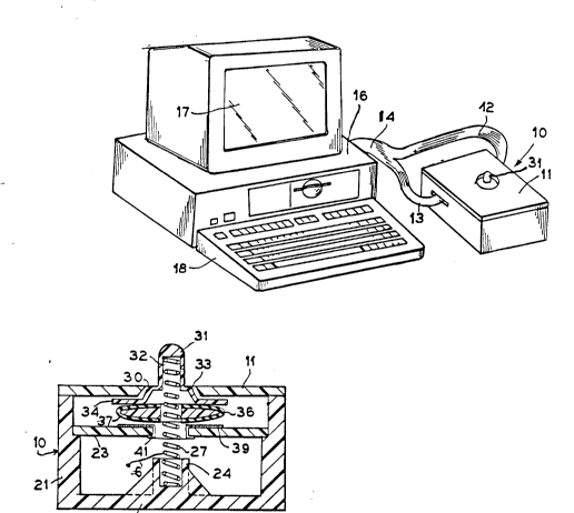
FIG. 1 is a perspective view illustrating the novel joy stick/pressure pad of the invention mounted
in a container 10 which has a top surface 11. Cables 12 and 13 extend from the container 10 and join in a
cable 14 that is connected to a micro-controller 16 that is associated with a monitor 17 and a keyboard 18.
FIG. 2 is a sectional view of the joy stick of the invention wherein the container 10 has a bottom 22
and side walls 21 and a top wall 11 formed with an opening 30. A spring 27 is mounted in a boss 24 formed
in the bottom wall 22 and extends upwardly through an opening in a printed circuit board 23 mounted in
container 10 and which has electrical conductive paths 41 and 39 formed on the inner surface ofthe opening
and the printed circuit board. A force diverter 36 is mounted on the spring 27 and at least the outer surface
is electrically conductive. It may be made, for example, of low durometer rubber and has a lower conductive
surface which can engage printed circuit paths 39 on the printed circuit board 23 when the spring 27 is
deflected from its center position. The spring 27 extends through the opening 30 in the top surface 11 and
a stick 31 has an opening 32 in which the spring is received. The stick has a downwardly extending
21 771 ~ 8
generally conical portion 33 which joins an outer flat portion 34 that engages the force diverter 36. When
the stick 31 is moved, it causes the spring 27 to be deflected so it engages the surface of the conductors 41
formed in the opening in the printed circuit board 23 and also causes the force diverter 36 to engage the
printed circuit paths 39 on the printed circuit 23. The container 10 may be made of non-conductive material
and an electrical voltage is applied to spring 27 by a conductor 6 so as to provide an energizing voltage.
FIG. 3 illustrates the joy stick 31 in a deflected from neutral position wherein the outer conductive
surface 37 of the force diverter 36 engages the printed circuit conductors 39 and a sheath 28 which is
electrically connected to the spring 27 makes electrical contact with one of the conductors 41 in the opening
in the printed circuit board. The center of the force diverter 36 may be hollow or filled with a suitable filler
such as plastic 38.
FIG. 4 illustrates a slightly modified form of the invention wherein the spring 47 has a first end 48
that is mounted by a sleeve 49 in a bottom plate 46 of the container 10, and the upper end of the spring is
received in the hollow insides 92 of a stick 51 which attaches to a bottom plate 53 which engages the force
diverter 54. The spring fits in the opening 92 in the stick 51. By moving the stick 51, the force diverter will
engage the conductive paths 39 on the printed circuit board 23 and the spring 47 will engage the conductive
paths 41 on the inside of the opening in the printed circuit board 23.
FIG. 5 illustrates a further modification ofthe invention wherein the force diverter 61 may be made
of a flexible substance such as low durameter rubber and has a portion which extends through an opening
in the printed circuit board and terrnin~t~C in an enlarged portion 62. A stick 63 extends through the opening
30 in the top cover 11 and has a lower flat portion 64 which engages the force diverter 61 to move it to
engage the circuit paths 39 on the printed circuit board 23.
21771 18
-
FIG. 6 illustrates in plan view the circuit board 23 and includes a first plurality of parallel conductors
121a through 121f mounted on a first segment portion of the board. A resistive path 126 extends at right
angles to the conductors 121 and makes electrical contact therewith. A second plurality of electrical
conductors are formed in another segrnent of the printed circuit board 123a through 123f and are de~ign~ted
122a through 122f and a resistive path 127 extends at right angles to the conductors 122a through f and
makes electrical contact therewith. A third plurality of conductors 123a through 123f are also mounted on
the board in a different segment and are electrically connected to a resistive path 128 which extends at right
angles thereto. A fourth plurality of conductors 124a through 124f are mounted on another segment of the
board 23 and are connPcted to a resistive path 129 which extends at right angles thereto. The spring 47 when
deflected engages the conductors 41 on the inside of the opening and the force diverter 54 engages the
printed circuit board.
FIG. 7 illustrates another arrangement of the printed circuit board 23 wherein a first plurality of
printed circuit paths in the form of segments of a circle 13 la-131i are formed in a first segment and are
traversed by resistive path 136. A second plurality of curved segments 132a-132i are formed on the printed
circuit board and are traversed by a resistive path 137. A third plurality of curve segments conducted paths
133a-133i are formed on the board and are traversed by resistive path 138. A fourth plurality of curve
segments 134a-134i are mounted on another segment of the printed circuit board 23 and are traversed by
resistive path 139. The opening through the printed circuit board is formed with four separate conductive
paths 101, 102, 103 and 104 which are separated from each other as shown.
FIG. 8 is a modification of the circuit board of FIG. 7 wherein a radially extending printed circuit
path 146 is mounted in the space between a first plurality of curved segments 141a-141e and a second
21 771 1 8
-
plurality of curved segments 142a-142e. Circuit paths 147, 148 and 149 extend from the radial circuit path
146 between the curved segments 141 and 142 as shown.
Other radial circuit paths 151, 156 and 161 extend through the gaps between the curved conductive
paths 142a-3 and 144a-3 as shown. Radial circuit path 151 has transverse extending conductive paths 152,
153 and 154 as shown. Radial circuit path 156 has transverse exten~ling circuit paths 157, 158 and 159 as
shown. Radial circuit path 161 has exten-ling transverse circuit paths 162, 163 and 164 as shown. The
spring 47 is engageable with the conductive segments 101, 102, 103 and 104 when deflected.
FIG. 9 shows another modification of the invention wherein circuit paths 216, 217, 218 and 219 are
interwoven between the curved circuit paths such as 213a-213f and 214a-214f and extend at angles which
are not perpendicular to radials so as to increase the quantity of speeds that are available in diagonals. It is
to be realized, of course, that the interwoven fingers such as 216-219 would also be formed between the
segments 212a-212f and 213a-213f as well as between the segments 21 la-21 lf and 212a-212f and also
between the segments 21 la-21 lf and 214a-214f.
FIG. 10 illustrates a printed circuit board 23 which is formed with additional separated curve
segments so as to increase the angular resolution of the device. First parallel curve segments 192a- 192i are
traversed by resistive path 181. Second segments 193a-193i are traversed by resistive path 182. A third
plurality of segments 194a-194i are traversed by resistive path 183. A fourth plurality of segments 196a-
196i are traversed by resistive path 184. A fifth plurality of radial segments 197a-197i are traversed by
resistive path 186. A sixth plurality of radial segments 198a- 198i are traversed by a resistive path 187. A
seventh plurality of conductive paths l 99a- l 99i are traversed by a resistive path 189 and a eighth plurality
21 771 18
of conductive paths 201a-201i are traversed by resistive path 191 as shown. This increases the angular
resolution of the device by a factor of two over the board shown in FIGS. 6 and 7 for example.
FIG. 13 illustrates in detail the manner of connecting the various electrical conductive paths to an
external circuit. The conductive portions 101, 102 and 103 and 104 formed in the opening of the printed
circuit board 23 are connected to termin~l~ as shown which are then cormected by conductive paths to
terminals such as 309. Curved segments 131 are each connected to different terminals and are connected
by leads such as 302 and 303 to different terminals 304. Other segments are each connected to different
terminals such as 306 which are connected to different remote terrninals 304 by conductive path 5.
Thus, the present invention provides a novel joy stick which allows many different orientations to
be recognized and sent to a control device, as well as allows the amount of deflection of the joy stick or
pressure pad to be detected, so as to provide a control signal.
FIGS. 14, 15 and 16 illustrate a modification which includes a substrate 401 upon which is forrned
an annular shaped resistive material layer 402.
Conductive pads 407,408,409 and 410 contact the outer edges ofthe layer 402 as shown. Electrical
leads 412, 413, 414 and 415 are respectively connected to conductive pads 407, 408, 409 and 410 as shown.
Digital input conductive traces 403,404,405, and 406 are formed on substrate 401 within the annular
shaped resistive material layer 402.
When deflected, the force diverter, not shown in FIGS. 14, 15 and 16 engages the resistive layer 401
at point (P) 417, for example, as shown in FIGS. 16 and 17.
The resistive value at point P can be found as shown in FIG. 17 in the following manner:
2~ 7~1 1 8
-
To find the co-ordinate of point P, we first find the shortest distance from a, b, c, d, using the analog
conversion. Once this is completed, we triangulate between the three closest points with respect to their
polar position. One example is as shown whereby point P is closest to point b in the upper left quadrant.
Our knowns are:
YT= COnStant
XT = Constant
Yl + Y2 YT
Xl + X2 = XT
-~/(Xl)2~ (Y1 ~ O ~YT)2l = a'
~/(Y2) + (0.5 XT - x~)2 1 = b
~/(x2)2+(y2)2l = c'
Thus, the voltage at contact point P can be determined relative to the contacts 407, 408,409 and 410 and
from these values, the position of point P can be determined.
Although the invention has been described with respect to preferTed embodiments, it is not to be so
limited as changes and modifications can be made which are within the full intended scope of the invention
as defined by the appended claims.