Note: Descriptions are shown in the official language in which they were submitted.
~ WO 95/15042 2 t 7 7 2 6 4 Pcr/u594/13601
APPARATUS AND MTeTHOD FOR
T.~T.TMT~rTI~ NAPPING JITTER
TEt'TlNTt'~T. FTTeT.I- OF 'I~TT' l~v~Ll~N
The pre6ent invention relates in general to
t~le: ;cations n~L..J.}~: and more particularly to an
Lu5 and method for eliminating mapping jitter.
I j ~ , . .
36560-1150 2 l 7 72 6 4 PCT~S 94~ 13 6 0 1
2 IPEA/us 2 2 JUN Igg5
BA~ ~u~ OF THE INVFNTION
A desynchronizer is a device that LeCuV:L_ an P~nhP~Pd
signal containing a~yllullLvlluus data at a specific clock
rate from wLthin a higher rate digital bit stream of a
~yll- IILO~UUS channel. The clock rate for the Pmhe~l iPd
signal is unrelated to the clock rate for the nyllullLulloug
channel. When the P~hP~l~lP~ signal is multiplexed into the
Yyll~llLulluus channel, it is necesclry to synchronize the
: -- ?d signal with bit or byte timing adjustments. The
process of recovering the asyn~ 1lLul-ous data and clock rate
of the - '~od signal is complicated by data gaps and
overhead timing adjustments ne~PCs~ry to map the P~he~lAPd
signal into the ~yl.~.l.Lulluus channel.
The conventional approach to ~ ting the
overhead gaps is to allow them to appear as fluctuations in
the instantaneous fill level of a data buffer referred to
as an elastic store. Clock Lec~ Ly is accomplished by
using the fill level of the elastic store to drive a low
pass filter, which in turn drives a voltage control
oscillator, to produce a desired clock signal for
nyll~ Lùl~uuS transmission of the data from the elastic
store. High frequency instal,~lneuus variations in the
elastic store fill value, due to the overhead gaps
installed during ~jyll~llLul~ization~ are filtered by the low
pass ~ilter but not completely eliminated. Napping j itter
remains on the output of the de-yll~:llLullizer due to
instantaneous variations in the elastic store f ill value
that are not fully filtered out. Therefore, it is
desirable to have a denyl-~ l.Lul~izer without any mapping
3 O j itter on its output .
From the foregoing, it may be appreciated that a need
has arisen for a deny..~ l.ru..izer device that eliminates
instantaneous variations in the elastic store f ill value
caused by overhead gaps on the nyl.. l.ru..uus channel. A need
has also arisen to remove mapping jitter from the output of
the denyll~llLullizer device.
AMENl~ED SHEET
~ WO95/15042 21 77264 PCT/USg4113601
6TTMMAT2V OF ~I'T-TT~ INVl;NTION
In accordance with the present invention, an apparatus
and method for eliminating mapping j itter are provided
which substantially eliminate or reduce di~adv-n~a~s and
problems associated with conv~nti~AnAl deay.. l,Lol.izer
devices .
According to an omho~l; L of the present invention,
there is provided an a~uAL-Lus for eliminating mapping
~itter that ;nr1~ O~ a ~ ~ circuit for reading
a~yll~llLulluus data and a clock rate of an omhe~lod signal
within an ~y11u11Lu11uus payload envelope received over a
~,y11u11lv1-uus channel and an elastic store circuit for
storing the aDyll~llLUllUUS data, ;nrl~l-l;nj overhead gaps and
timing adjustments, read by the 1 , circuit according
to the clock rate of the omhP~locl signal. Instantaneous
variations due to overhead gaps in a fill value of the
elastic store circuit are detorminocl by an overhead gapfill
circuit . A mapping j itter elimination circuit eliminates
the instAntAnooll~ variations r~Pt_rm; nod by the overhead
gapfill circuit in order to recover an output clock rate
for the y11u11Lu11uus transfer of ~..y11u11Lu11ous data from the
elastic store circuit.
The apparatus and method of the present invention
provide various torhn; ~AA 1 advantages over convont; ,A,llA 1
de_yll~llLullizer devices. For example, one terhn;rAl
adv~..Lag~ is in ~otorm;n;nj the in~,La--Lu,-eous variations in
the fill value of the elastic store circuit due to vvt:Ll-ead
gaps placed in the ~ signal during Dyll-,llL u..ization.
Another terhn;rAl advA--La~ is in eliminating the
instantaneous variations in order to recover an output
clock rate for the Dy11ul1Lu11uu~ transmission of the
aDyll~;llLUllUU~ data within the elastic store circuit. Yet
another technical advantage is in eliminating mapping
~itter from the LeCuv~Led output clock rate of the
deDy-.u1.Lu-.izer device. Other torhn;~AAl advantages are
WO 95115042 2 1 7 7 2 6 4 PCrNS94/13601 ~
readily ~a~ellL to one skilled in the art ~rom the
following ~igures, descriptions, and claims.
~ wo 9S/1504~ 2 1 7 7 2 6 4 PCT/USg4/13601
FIRT~F r)ES~RTPTION OF T~E DR~wJNGs
For a more complete understanding of the present
invention and the advantages thereof, reference is now made
to the following description taken in cv..ju--~ Lion with
~ _ nying drawings, wherein like reference numerals
:e~LeSellL like parts, in which:
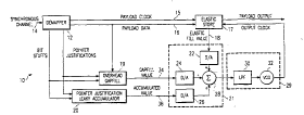
FIGURE 1 illustrates a block diagram of a
d~ay-~ ul~izer device;
FIGURE 2 illustrates a diagram of an: ` -'' 1 signal
lû mapped into a ayllo11~ulluus payload envelope;
FIGURE 3 i6 a timing diagram illustrating an ~nhs-nrl~l
operating mode of the deay-.. 1~, ul.izer device; and
FIGI~RE 4 is a simplif ied schematic diagram of a low
pass f ilter within the deay-..l.L u..izer device .
21 77264
- 36560--1150 4 -- i .~ L
6 IPEA/l~
D~TATT T'lf DESt`PTPTION OF 'I~IT~' TNvENTIoN
FIGURE i is a block diagram of a deay..ul.ru.lizer device
10 . Desynchronizer device 10 ; n~ Pc a demapper circuit
12 that receives Yyll~ t u-.uus data at a _yllul~lùl-uua clock
rate over synchronous channel 14. Demapper circuit 12
extracts a payload clock 15 and a payload data 16 for an
'--''-' signal within ay~ Lulluus channel 14. Payload
data 16 is buffered within an elastic store circuit 17
according to payload clock 15. Elastic store circuit 17
generates an elastic fill value 18 indicating a depth of
asynchronous data wlthin elastic store circuit 17.
Demapper circuit 12 generates bit stuf f and pointer
justif ication outputs for use by an overhead gapf ill
circuit 19 and a pointer justification leaky AC, lator
circuit 20. Outputs of elastic store circuit 17, overhead
gapfill circuit 19, and pointer justification leaky
a~ lator circuit 20 enter a mapping jitter elimination
circuit 21 and pass through digital-to-analog converters
22, 24, and 26, respectively, and are combined at summing
node 28. The combined output from summing node 28 enters
a clock recuv~ly phase lock loop circuit 29 and are
filtered by a low pass filter 30 to drive a voltage
controlled oscillator 32. Voltage controlled oscillator 32
generates an output clock signal to _yll- llLUllUU~ly transmit
a payload output 33 from elastic store circuit 17.
In oper~tion, desynchronizer device 10 iterates on a
specific number of bytes on ~y~ollrulluus channel 14 for a
predet~rm;n~l interval. The nominal frequency of the
yll- llr~lluus channel is 51. 84 NHz . FIGURE 2 is a diagram of
how the ~mh~ d signal is mapped into a :~yl-ullrul~ous
payload envelope of the synchronous channel as def ined by
the ~yll-llrulluus optical network (SONET) specification. The
ayll~ ulluu5 payload envelope includes 90 bytes; 3 bytes of
transport overhead, 1 byte of path overhead, and 86 bytes
of the mapped ~mhorl~ecl signal. Nine ayll~llLùllOus payload
envelopes make up a single frame on :-yllullLullous channel 14
AMENOE~ SffEET
_ _ _ _ _ _ _ _ _ . . . ,, ., .,,, ,, . ,,, . , _ .. ,, . , . _ . ,
36560-1150 2177264 j~,~'T,i~ 94113~1
of FIGU~E 1. The ~ od signal is mapped with
information bits, fixed stuff bits, stuff control bits,
stuff U~J~JUL Lul~ity bits, and overhead control bits.
Demapper circuit 12 ~Locesses information on
:.yl.~ l.Lùl~uuS channel 14 by extracting a synchronous payload
envelope and then extracting the asyn~ l.L~uuS data and
clock rate of the o~he~ ocl signal within the synchronous
payload envelope. Demapper circuit 12 generates payload
data 16 and payload clock 15 of the omho(~rlod signal for use
by elastic store circuit 17 for storage of the asynchronous
data . Demapper circuit 12 also provides bit stuf f and
pointer justification outputs which indicate whether or not
timing adjustments have occurred during an iteration
interval .
Elastic store circuit 17 is an up/down ~ tor
which accepts bit count in-iL~ ts from ,1 ror circuit 12
and bit count dec~L~ - from voltage controlled oscillator
32. Elastic store circuit 17 maintains a running count of
the difference between the number of received payload data
bits and the number of transmitted payload data bits. The
following ~ c-lccl nn as6umes that elastic store circuit 17
has a capacity of 512 bits, allowing a fluctuation of +/-
256 bits.
Overhead gap~ill circuit 19 calculates the effect of
overhead gaps within the omhe~l~ocl signal. Overhead gaps
neCoccii~ry to map the ai~yllcllLu~luus data to synchronous
payload envelopes within ay..~ l.Lvlluus channel 14 cause
instantaneous variations in elastic fill value 18 of
elastic store circuit 17 that do not reflect changes in the
clock rate. Typically for the omhod~o~ signal, these
overhead gaps occur at an 8 kilohertz rate and can be
filtered out by low pass filter 30 of clock recu~Ly phase
lock loop circuit 29. EIowever, adequate elimination of the
effects of the overhead gaps requires a very low bandwidth
phase lock loop on the order of 1 hertz. Wider bandwidth
filters would be easier and more ocn~ ici~l to implement
~ WO9S/ISo42 2 1 7 7 2 6 4 PCr~US9~J13601
than such a low bandwidth filter. Overhead gapfill circuit
19 allows for the impl Lation of wider bandwidth
f ilters .
Overhead gapfill circuit 19 l~oduces a gapfill value
to effectively eliminate the overhead gaps from entry into
low pass filter 30 and voltage controlled oscillator 32 of
clock L~Cuve:~y phase lock loop circuit 29. Gapfill value
34 is combined with elastic fill value 18 of elastic store
circuit 17 to eliminate the overhead gap contribution to
elastic store circuit 17 before it can ~uual~a~e through to
low pass filter 30 and voltage controlled oscillator 32 of
clock recovery phase lock loop circuit 29. Overhead
gapfill circuit 19 calculates gapfill Yalue 34 from the
following equation:
gapfillfi=~prf; 7 7" 1+ (6 . 9 ~7BPI) +BSD ~1)
+ [ ( 2 07 /29 ) PJ] - NBITS
5
where, gapfilln_1 is the previous gapfill value,
(6 . 9 NBPI) is an l-e~ l~cl number of data bits per
~y~ Lulluu:, channel byte (information bits/bytes
in syn~ ul.uus payload envelopes =
5+20o+92oo8+2o8=6~9) multiplied by number of
~yll~:llr u--uu~ channel bytes ~Lo~essed in each
iteration,
BSD is the number of data bits occurring in the bit
stuff position,
[ (207/29) PJ) ] is an expected number of data bits in
an
extra pointer justification byte (information
bits/bytes of ~ signal = 6871 = 22097 )
multiplied by a pointer justification flag
(+1 for added data byte, O for no adju~-i , and
~ Wo 9S/15042 2 1 7 7 2 6 4 Pcr/uS9~/13601
-1 for stuff data byte), and
NBITS is the number of: '~''^~ a~y~lul~rulluus data bits
received in the elastic store circuit during the
iteration interval.
ûverhead gapfill circuit 19 receives the number of
bytes processed, the number of bit stuffs occurring, and
the pointer justification flag from t~ _, circuit 12.
ûverhead gapfill circuit l9 ~lDtprminpc the effect of an
overhead gap by ~ietPrm;n~n^; the average number of data bits
that should be received in the interval and subtracting the
number actually received. The calculated value is added to
the previous value to maintain an ~ ted phase shift.
Timing a,l; u~ t. due to bit stuf f 5 and pointer
justif ications rt:uLa5~ ins~Ant~np~ c phase shi~ts in the
: '~P-l signal data stream which also produces
Lallkllle~/u~ changes to elastic fill value 18 of elastic
store circuit 17. The effects of these inDLa--Lc...auus phase
shifts can be sufficiently smoothed if a very low loop
bandwidth, a small fraction of a hertz, is i _ l Led in
low pass filter 30 and voltage controlled oscillator 32 of
clock Le~uv~=Ly phase lock loop circuit 29. To avoid having
a very low loop bandwidth and allowing for the use of a
less stable voltage controlled oscillator, the timing
adjustments can be digitally filtered. Pointer
justif ication leaky ~ tor circuit 20 R . _ ' Les
this by n~ 1 ~ting recent pointer justif ication timing
2dju~; Lt, and subtracts them from elastic fill value 18
of elastic store circuit 17. In this manner, recent
pointer justification timing adju~l Ls are removed from
the input to clock r~uvve:Ly phase lock loop circuit 29 of
low pass filter 30 and voltage controlled oscillator 32.
An a~L l~ted value 36 detPrm;npc~ by pointer
justification leaky n~ l~tor circuit 20 is allowed to
decay at a very slow rate, referred to as frArtion~l bit
leaking, to allow clock Lecuv Ly phase lock loop circuit 29
to ~t -'~te the phase adjustments on a gradual basis.
21 77264
W09~/~5042 PCrll1S94/13601
The equation executed by pointer justification leaky
accumul~tor circuit 20 once per iteration i6:
PJAn=PJAn l- [sig7l0f(P~JAL l) (MIN~as(PJAn 1) ) (2)
(SC~LE/1024) ] - (7 p~
where, PJAn_1 is the previous pointer justification
~ ted value,
NIN is a ,,UL UyL hl P minimum leak rate (where 10 is
a nominal value,
SCALE is a ~LVyL hlP factor (1, 2, 4, 8) that
allows for accelerated leaking, and
PJ is a pointer justification flag (+1 for added data
byte, 0 for no adju~ L, and -l for stuff data
byte .
The NIN value, scale factor, and 1024 divisor are
designated for executing leak calculations at 1 Tn~ cpcnTl~
intervals. A pointer justification timing adju~ L
UIJUUL Lullity~ the time where PJ may have a non-zero value,
occurs once every 500 micrss~ nn~lC. The accumulated PJA
value is inverted by the term (7 PJ) to allow for positive
summation in circuitry external to the digital logic, such
as at summing node 28.
Digital-to-analog converter 22 converts elastic f ill
value 18 of elastic source circuit 17 to analog f orm by
dividing the fL~4Uell~:y of a most significant bit of an
elastic store circuit 17 write address by 2 and exclusive-
or'ing this result with a most significant bit of an
elastic store circuit 17 read address divided by 2. For an
elastic store circuit 17 having a store size of 512 bits,
the most significant bits change state once every 11.44
microsecnnAC (elastic store capacity of 512 bits/nominal
center rLeyue~ y of voltage controlled oscillator 32 of
44.736 NHz). Nore frequent measures of elastic fill value
18 of elastic store circuit 17 may be obtained by
~ WO 9~1l5042 2 1 7 7 2 6 4 PcrluS94113601
11
implementing an ~nh~n~-ed mode that use6 less significant
bits in the ad.lLe~c~s. This ~nh;~ln~ l mode inserts extra
speed up or slow down transitions in elastic f 111 value 18
of elastic store circuit 17 in between changes of state of
the most signif icant bits . Since t_e ~nh~nred mode
provides more gain for small phase offsets but less dynamic
range, it may be desirable to disable the ~nh~nred mode
during phase lock loop initialization. FIGURE 3 shows the
timing diagram for the speed up and slow down transitions
of the ~nh51n-~ed mode implementation that may be performed
by digital-to-analog converter 22.
Digital-to-analog converter 24 generates a pulse width
modulation output containing gapfill value 34 of overhead
gapfill circuit 19. Gapfill value 34 is generated once
every 3 . 086 seconds or every 20 ~yllcllL~ U5 channel bytes
at digital-to-analog converter 24. Digital-to-analog
converter 26 generates a pulse width modulation output
containing ~ ted value 36 from pointer justification
leaky ? ~ tor circuit 2 0 . ~ ted value 3 6 is
gelleL~Ited once every 1 mi11; ceCon~l at digital-to-analog
converter 26.
FIGURE 4 is a c; _lif;ed diagram of low pass filter
circuit 30. Low pass filter circuit 30 ;nrl~ c resistors
R1, R3, and R4 tied to elastic fill value 18, a: l~ted
value 36, and gapfill value 34, respectively, which are
tied to summing node 28. A resistor R2, a capacitor C, and
an operational amplif ier 38 make up the low pass f ilter
l- of low pass filter 30. The three input
resistors R1, R3, and R4 provide the summing function of
summing node 28 as well as contributing to the definition
of the loop bandwidth ~n. Clock rec~v~Ly phase lock loop
circuit 29 of low pass filter 30 and voltage controlled
oscillator 32 is a conventional second order phase lock
loop defined by a low pass filter transfer function:
21 77264
36560-1150 ~ i ~ U ~
12 IPEA/US 2 2 J~N 1g95
- F(s) 5 1 T, ~3)
and open loop transfer function:
G(s) 5 Rd F(s) Ko( 1) = ~ n n t4
and a closed loop transfer function:
N(~) = 2 ~n n 2 (5)
where,
Tl = Rl C which equals a loop time constant in seconds,
T2 ' R2 C which equals a loop time constant in seconds,
Kd is the phase detector gain in volts per cycle,
Rl is resistance in oh~ns,
R2 is resistance in ohms,
C i8 capacitance in ~arads,
Ro is the VC0 gain factor in hertz per volt,
Fo is the VC0 center frequency in hertz,
RA is equal to Kd-Ko which is the loop gain in hertz
per cycle,
~n ls equal to the sguare root o~ KA divided by T1
which is the closed loop natural f requency in radians per
second,
~ is a constant,
LDR is equal to ~n T2 divided by 2 which is the loop
damping ratio .
Resistor R3 iB identical in value to resistor R1. The
value of resistor R4 is determined such that equal input
AMEN~iEO S~i'Er
. . _ _ . _ . _ . _ _ _ _ _ _ _ .
21 77264
36560--1150 ., -8
13 PEq~UJ
current~ ~low through each of resistors Rl, R3, and R4.
Gapfill value 34 is pulse width modulated with each new
calculation of gapfill value 34 for combination to elastic
rill value 18 of elastic store circuit 17 and ~rc~ ted
value 36 of the timing adJu~i ts. For an overhead
gapfill circuit 19 having a 12 bit width (11 bits of
magnitude and 1 bit of polarity), the seven most
signiricant bits are used with the 51. 84 r~Hz clock of the
~iyll~.llLUl~ous channel and the pulse width modulator is scaled
to 128 counts out of 160 counts in an interval. Elastic
fill value 18 of elastic store circuit 17 has a voltage
range of 2 . 5 volts for a full scale value of 256 and
2.5/256 volts per bit. Gapfill value 34 has a voltage
range of (128/160)-2.5 = 2 volts for a full scale value of
2048/29 and 29/1024 volts per bit. For equal input
currents per bit into summing node 28 (2 . 5/256) /Rl must
equal (29/1024)/R4. Hence R4 = (29/10)-Rl. Table I shows
representative values of selected loop parameters.
Tl~BLE I
Rl = 15K c=0 . 331-f
R2 = 499K Kd = 8 . 8 volts/UI
R3 -- 15K XO ~ 955Hz/v
R4 -- 43 . 2K Jn = 41. 2 rps
LDR -- 3.39
Though specific values for certain parameters are shown,
none of the parameter tolerances are critical except for
the ratio R4/Rl = 2 . 9 .
De~y.. ~l.Lul~izer device 10 ~,u-luces output jitter from
three different sources - mapping jitter due to overhead
gaps, waiting time jitter ~Luduced by bit stuffing
u~u~c,L Lul,ities, and j itter ~ luced by pointer
~ustifications. Overhead gapfill circuit 19 detDrm;nDc
gapfill value 34 to account for the effect of the overhead
gaps and eliminate mapping j itter from the output of
~ WO95/15042 2 1 77264 PC'r/US9.t~1360~
14
de~,yllo1.Lvllizer device lO. Similarly, pointer justification
leaky ~ tor circuit 20 llt~t~rm;nt~c :~rc~ ted value
36 and fractlonal bit leaking allows clock Le~uvt:Ly phase
lock loop circuit 29 to ~ te the phase F-lJu-i ~8
on a gradual basis to reduce the effect of pointer
justification jitter on the output of deayll..l.Lu.lizer device
lO. Pointer justification leaky ~,: lAtor circuit 20 may
also account for the waiting time jitter by inrlllA;n~ bit
stuff in~ L Ls in equation 2. The new equation to
account for bit stuff in~:L~ L5 is:
PJAn=PJAL l- [signof(PJAn l) (~in+abg(P~TAn-1) ) ~6)
(SG~LE/1024) ] - (7-PJ) -BSA
where BSA is a bit stuff adjustment value indicating a
variation from a nominal stuff ratio of 2/3 (BSA =
+2/3 for data bit in stuffing U~J~)UL Lu..ity, 0 for no
stuffing opportunity, -l/3 for stuff bit in stuffing
U~ )L Lu--ity) .
The fractional bit leaking of the n~ l ~ted value will
also reduce the waiting time jitter due to bit stuffs
through this t~nhAnrt~ addition to the equation for pointer
justification leaky ~t l~tor circuit 20.
In summary, a de~y-..:l.Lv-lizer eliminates mapping jitter
on its output by calculating the overhead gaps in an
I ,h~ lt~Cl signal mapped into a :~yll~l~Lul-ûus channel. These
overhead gaps cause inst:~n+~nt~o~C variations in the elastic
fill value of an elastic store circuit which propagate onto
the payload output resulting in the mapping j itter. An
overhead gapfill circuit uses bit stuff outputs, pointer
justification outputs, and data outputg from a tA- ~
circuit to calculate a gapfill value for the overhead gaps.
The gapfill value is added to the elastic fill value of an
elastic store circuit to eliminate the i~ t~t llc
variations due to overhead gaps from entering into a clock
~ Wo 9511So42 2 1 7 7 2 6 4 PCT~US94/13601
recuvury phase lock loop of a low pass filter and a voltage
controlled oscillator. Jitter from bit stuffing operations
and pointer justirications are reduced by eliminating an
A~ ted value ~t~rmin~d by a pointer justii~ication
leaky ~ tor circuit frûm the elastic fill value Or
the elastic store circuit prior to ; r~ Lation of the
low pass ~ilter and voltage controlled oscillator of the
clock recovery phase lock loop.
Thus, it is a~ar~ L that there has been provided, in
accordance with the present invention, an auua- aLus and
method for eliminating mapping jitter that satisfy the
advall~a~s set forth above. Although the preferred
Pmho,7 i ~ L has been described in detail, it should be
understood that various changes, substitutions, and
alterations can be made herein. For example, though
speciric values and timing intervals have been ~; CC71qqc~
alternate values and timing intervals may be used with
similar effectiveness. Fur~h a, analog summation as
~mhot9ied in summation circuit 21 can be implemented
digitally. Other changes may be made by one skilled in the
art without departing from the spirit and scope o~ the
invention as defined by the following claims.