Note: Descriptions are shown in the official language in which they were submitted.
CA 02177275 2003-12-09
~'L3 95115673 PC."TlUS931116$4
1 FABRICATION MULTILAYER COMBINED RIGID/FLEX
2 PRINTED CIRCUIT BOARD
3
4 Background of the Invention
Field of the Invention
6 The present invention relates to the fabrication of
7 multilayer combined rigid and flex printed circuits having
8 flexible printed circuits extending from the rigid board.
9 In particular, the present invention relates to an
improved process for the fabrication of multilayer
11 combined rigid and flex printed circuits, wherein two
12 circuit boards having rigid and flexible sections can be
13 prepared from a novel basestock composite.
14 Background of the Invention
Techniques for making multilayer rigid flex printed
16 circuit boards are well known in the art. One early
17 example of the prior art is disclosed in U.S. Patent No.
18 3,409,732, assigned to the Assignee of the present
19 application. Typically a rigid flex stacked printed circuit
21 board includes flexible printed circuit cables extending
22 from the periphery of the rigid section or sections. The
23 rigid portions of the flex cables are typically used as
24 sites for electronic components or mechanical hardware.
It is important to note that the copper conductor in each
26 plane or layer is fabricated from one continuous sheet of
27 copper foil.
28 With improvements in electronic technology, there has
29 been a constant need for advances in electronic packaging.
This need has led to more complex multilayer rigid flex
31 printed circuit boards with many boards now using up to
32 twenty-five, or even more, layers of circuitry. However,
33 severe problems developed when the rigid circuit portions
34 included many layers of conductors and holes plated
through with copper to provide conductor barrels
36 connecting the conductor layers.
CA 02177275 2003-12-09
-2-
1 One particular problem, reported on and discussed in
2 U.S. Patent No. 4,800,461, assigned to the assig~me of t3te
3
present Application, described the fact that in multilayer rigid
4
flex boards cahich included insulator materials such as
6 acrylic adhesive and Kapton (Kapton is a trademark of E.I.
7 duPont de Nemours and Company Inc. for polyimide film),
8 the insulating materials placed a "Z-axis" stress on
9 plated through holes. The coefficient of thermal
expansion, it was reported, of the acrylic adhesive (Z-
11 axis expansion) was the dominate influence. It was
12 observed that because of the amount of acrylic required in
13 many multilayer rigid flex applications, all plated
14 through holes are stressed, with many cracking, making the
boards unusable.
16 To overcome this problem, the '461 patent reported on
17 a novel process to provide a rigid section incorporating
18 insulator materials which, when subjected to elevated
19 temperatures, did not expand in the Z direction to cause
difficulties, including delamination and cracking of
21 plated copper barrels. Stated another way, in the '461
22 patent,the materials causing undesirable expansion in the
23 Z direction in the multilayer rigid section of the board,
24 and the materials absorbing excessive amounts of moisture,
such as acrylic adhesives and Kapton, were eliminated from
26 the boards rigid section.
27 However, although the '461 patent was extremely
28 successful in addressing the various problems recited
29 therein, and in particular, the problem of thermal
stresses described above, the process for fabrication of
31 the rigid flex printed circuits has remained limited to
32 the fabrication of a multilayer combined rigid and flex
33 printed circuit board wherein two circuit boards are
34 always prepared from a basestock composition, and remain
attached to one another via the prepreg. In other words,
36 the process of fabrication according to the teachings of
WO 95/15673 2 1 7 l 2 l 5 p~~g931II684
-3-
1 the prior art begin with the step of laminating two
2 conductor layers (i.e. copper layers) to a single
3 insulator layer (prepreg) followed by imaging and etching.
4 Accordingly if one of the two bonded conductor layers was
somehow improperly imaged, it was necessary to discard the
6 entire lamination.
7 It is therefore an object of this invention to provide
8 a process for the fabrication of a multilayer combined
9 rigid and flex printed circuits, wherein two circuit
boards having rigid and flex sections can be prepared and
11 imaged from a novel basestock composite, followed by
12 separation into two individual single sided basestock
13 laminates.
14 It is also an object of this invention to provide a
novel basestock composition of sufficient planarity and
16 rigidity to permit adequate handling and further
17 processing thereof, and which can be separated into two
18 individual layers each comprising an imaged copper layer
19 laminated to a fiberglass sheet which is impregnated with
adhesives such as an epoxy.
21 Summary of the Invention
22 The present invention provides a multilayer rigid flex
23 printed circuit board fabricated by a novel process and
24 from a novel basestock composite wherein two copper sheets
are laminated to a prepreg and in-between said laminated
26 copper sheets is placed a release material that is not
27 coextensive with the boarders of the prepreg, such that
28 the basestock can be imaged and processed in the usual
29 manner, and such that cutting the edges of the basestock
material, after imaging, at a location internal to the
31 basestock border provides a cut into the release layer,
32 thereby allowing for separation of the two individual
33 imaged copper layers and their supporting prepreg, along
34 with the removal of said release material.
The present invention also comprises in process form,
36 a process for the fabrication of a rigid flex printed
WO 95!15673 217 7 2 7 5 pC.L~s93111684
-4-
1 circuit comprising the steps of laminating a pair of
2 conductor layers to respective opposite surfaces of an
3 insulating layer wherein the insulator layers are both
4 affixed to a release layer and wherein said release layer
is not coextensive with the borders of the insulator
6 layers, thereby forming a basestock composite. The
7 basestock composite is-then imaged and etched on the
8 conductor layers to form conductor patterns. The
9 basestock is then cut at a point internal to its borders
and into the release layer thereby separating the two
11 imaged and etched conductor layers and removing said
12 release material from the insulating layer.
13 Alternatively, the novel basestock composite can be
14 made without a release .layer, and such a basestock
composite which contains two copper layers permanently
16 affixed to one another, or the single copper layer
17 prepared from a basestock composite containing a release
18 layer, can be converted into a novel multilayer rigid flex
19 printed circuit board.
Brief Description of the Drawin s
21 The foregoing and other features and advantages of the
22 present invention will be more readily understood and will
23 become apparent from the following detailed description
24 taken in conjunction with the drawings, in which:
Fig. 1 is an exploded view of the novel basestock
26 composite.
27 Fig. 2 is an exploded view of the novel basestock
28 composite showing it cut at a point internal to its
29 borders and into the release layer.
Fig. 3 is an exploded view of the novel basestock
31 composite with a prepreg and Kapton/acrylic covercoat.
32 Fig. 4 is an exploded view of a single conductor layer
33 used to fabricate a multilayer combined rigid and flex
34 printed circuit.
Fig. 5 is a view in perspective of the layers of Fig.
36 4 following lamination and certain processing steps.
WO 95115673 2 1 7 l 2 7 5 PGT/US93/I1684
-5-
1 Fig. 6 is a cross section taken along view line 3-3 in
2 Fig. 5 and enlarged for clarity.
3 Fig. 7 is a perspective view diagrammatically showing
. 4 the inventive rigid flex circuits following lamination and
other processing steps of the structures shown in Figs. 5
6 and 6.
7 Fig. 8 is an exploded view of the sheet materials used
8 to form the layers of structures forming the inventive
9 rigid flex circuits, wherein the basestock contain two
laminated copper sheets without a release layer.
11 Fig. 9 is a view in perspective of the layers of Fig.
12 8 following lamination and certain processing steps.
13 Fig. 10 is a cross section taken along view line 3-3
14 in Fig. 9 and enlarged in the interests of clarity.
Fig. 11 is a perspective view diagrammatically showing
16 the inventive rigid flex circuits following lamination and
17 other processing steps of the structures shown in Figs. 9
18 and 10.
19 Detail-ed Description of the Invention
In the first exemplary embodiment of the invention
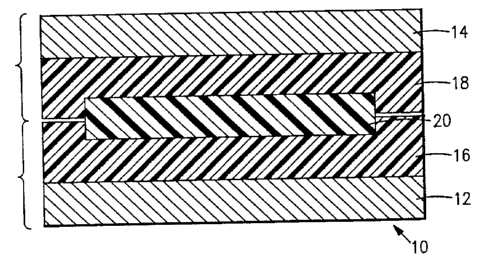
21 shown in Fig. 1, the novel basestock composite 10 is shown
22 to comprise two copper conducting sheets 12 and 14, for
23 example, one or two ounce copper, bonded to insulator
24 layers 16 and 18 comprised of fiberglass sheets
impregnated with an adhesive such as epoxy, and commonly
26 referred to as prepreg. Also shown in Fig. 1 is the
27 release material 20 and the release material is shown as
28 not being coextensive with the borders of the insulating
29 layers 16 and 18.
Accordingly, it can be appreciated that in the method
31 of preparation of-the novel basestock composite 10, a pair
32 of conducting sheets or layers, 12 and 14, are laminated
33 to the opposite surfaces of insulating layers 16 and 18,
34 wherein the insulating layers are both affixed to a
release layer 20 and wherein said release layer is not
36 coextensive with the borders of the insulating layers. It
2177275
WO 95115673 PCT/US93/11684
-6-
1 can be appreciated that the basestock composite comprising
2 the pair of conducting sheets has sufficient planarity and
3 rigidity to permit handling and further processing
4 thereof, and in particular, imaging to form conductor
patterns.
6 Turning then to Fig. 2, the basestock composite which
7 has been imaged and etched to form conductor patterns 22,
8 is cut at a point internal to its borders 24 and into and
9 through the release layer 20 and the two conductor layer
patterns 26 and 28 are separated and the release material
11 is removed from the insulating layers. Each conductor
12 layer can then be further processed, as described below.
13 Figure 3 shows one of the separated conductive layers
14 14 and its adjacent prepreg 18 further covered with
another prepreg layer covercoat 30 and a flexible
16 insulating layer of aKapton/acrylic covercoat 32.
17 Alternatively, the Kapton/acrylic covercoat 32 can be
18 replaced with a less expensive photoimagable solder mask.
19 In an exemplary embodiment of the invention shown in
Figs. 4-7, the formation of-the multilayer rigid flex
21 printed circuits begins with supplying a conductor pattern
22 26 or 28 followed by an initial processing step which
23 includes treating the exposed copper conductor patterns to
24 enhance bondability of another epoxy prepreg to the
copper, for example, by the black oxide process typically
26 used in the rigid board-field. One additional insulator
27 prepreg sheets 34, having cutout 38, is positioned on one
28 side of the base stock 26. A flexible insulator of Kapton
29 42, covered with a layer of suitable adhesive 44, for
example, an acrylic-adhesive which provides excellent '
31 bonding of Kapton to copper, is positioned on one side of
32 the glass sheet 34. A similar sheet of Kapton 46 covered "
33 with a layer of adhesive 48 is located on the other side
34 of the glass sheet 26. Insulator layers such as Kapton
and acrylic adhesive afford flexibility and tear
36 resistance characteristics to the flex sections, as
W O 95f 15673 217 7 2 7 5 p~YUS93I11684
_7_
1 discussed in connection with Figs. 6 and 7.
2 Alternatively, the Kapton 46 and adhesive 48 can be
3 replaced with a photoimagable solder mask.
4 As shown in Fig. 6, the Kapton sheets 42 and 46 and
their associated adhesive layers 44 and 48 are slightly
6 longer than the length of the cutouts 38 and 40 in the
7 glass layers to overlap slightly the sheet 34 by, for
8 example 0.050 inch. The sandwich formed by the foregoing
9 sheets is then laminated together to provide the printed
circuit structure 50 shown in Figs. 4 and 5. Note that in
11 the interests of clarity, the sides of the cutouts are not
12 shown in Fig. 7.
13 After lamination processing, a number of the printed
14 circuits 50 are stacked in proper registration with epoxy
impregnated fiberglass layers 52 (Fig. 7) positioned
16 between, for example, seven of the circuits 50. For
17 clarity, only two of the printed circuit structures 50 are
18 shown with the upper circuit 50 illustrated
19 diagrammatically and broken away.
Note that cutouts 54 in the prepreg sheets 56 are
21 slightly longer than the cutouts 38 (Fig. 4) and
22 coextensive with the Kapton layers 42 and 46 so that the
23 Kapton layers 42 and 46 abut the edges of the sheets 56,
24 as shown in Fig. 7.
Prior to stacking the circuits 50, it is desirable to
26 cut the flex cables, shown in Fig. 7, that extend through
27 the cutout areas, to simplify the final construction of
28 the rigid flex printed circuit structure.
29 After stacking seven of the circuits 50 with
' 30 appropriate outer caps, the layers are laminated to
31 provide, in this example, a nine layer rigid flex circuit
32 (the outer caps add in this example one layer per cap),
33 and holes are then drilled at appropriate pads 58 to
34 interconnect desired conductors 60. The holes are then
desmeared by a suitable process, for example, exposing
36 them to appropriate cleaning chemicals to expose fully the
2177275
WO 95!15673 PCTIU593/11684
_g_
1 copper conductors, a rapid process due to the absence of ,
2 any adhesives or insulating material resistant to such
3 chemicals, such as acrylics and Kapton, in the rigid
4 circuit portion. If desired, plasma desmearing techniques
can be used instead of chemical cleaning.
6 The holes are then plated through to interconnect
7 desired conductors 60, a portion of a plated-through
8 barrel 62 being shown in broken lines in Fig. 6, because
9 it will not be formed until after lamination of the
circuits 50 with the prepreg layers 56.
11 Referring next to Fig. 7, which shows somewhat
12 diagrammatically a rigid flex circuit 64 with the plated
13 through holes 62 enlarged, in the interests of clarity,
14 flex cables 66 coextensive with the rigid and flex
sections, and extending between the rigid sections 68 and
16 69 for suitably connecting the printed circuits. If
17 desired, upper and lower caps are laminated to the
18 circuits 50 in the rigid board area 68 only. Such caps
19 typically are fabricated using polyimide glass or epoxy
glass copper-clad laminates. Copper conductor circuits
21 can be formed on one or both sides of the caps, as
22 desired.
23 With the rigid section 68, and the portions of the
24 flex cables coextensive with the rigid section, formed by
an insulator material, i.e., layers of fiberglass and
26 adhesive, such as epoxy, which have characteristics or
27 properties which allow the rigid-board portion to relieve
28 stresses, caused by heating, in the board, delamination of
29 the circuits and cracking of the plated through barrels is
prevented when the board, or portions thereof,-is
31 subjected to elevated temperatures.
32 In other words, the rigid board 68 does not contain
33 troublesome materials, such as acrylic adhesive and
34 Kapton, having high expansion rates and moisture
absorption properties, because the flex cable sections
36 including Rapton and acrylic adhesive only extend to but
WO 95115673 2 1 7 7 2 7 5 PCflUS93/11684
_g_
1 not substantially into the rigid section. Of course the
2 Kapton and acrylic layers could extend an insubstantial
3 distance into the rigid section without causing undue
4 problems. Further, subjecting the inventive circuits to
hot solder reflow and elevated temperatures will not cause
6 differential expansion and contraction leading to cracking
7 of the copper plated through barrels 62 or delamination of
8 the layers. Moreover, extended baking times at
9 temperatures on the order of 250°F., often as long as 48
hours, to remove moisture, are avoided. Additionally, and
11 advantageously, use of release and/or carrier board
12 materials in the base stock portion of the inventive board
13 permits increased rigidity and better handling
14 characteristics of thereof.
While the invention enables the successful fabrication
16 of multilayer rigid flex boards having a great number of
17 conductor layers, the invention also provides excellent
18 multilayer rigid flex boards having fewer layers, for
19 example on the order of as few as four conductor layers.
In the second exemplary embodiment of the invention
21 shown in Figs. 8-11, the initial processing step includes
22 forming base stock 70 by laminating two copper sheets 72
23 and 74, for example one or two ounce copper, to an
24 insulator layer 76 comprised of one or two fiberglass
sheets impregnated with an adhesive such as epoxy,commonly
26 referred to as prepreg. While two layers of glass have
27 been shown, in order to provide at least 3.5 mils between
28 the copper planes after lamination, for meeting military
29 specifications, a single sheet of prepreg may be used in
appropriate circumstances.
31 Following lamination of the base stock 70, the copper
32 layers are imaged and etched to provide copper pads 78 and
33 conductors 80 (shown diagrammatically in Fig. 9) on the
34 glass layer 76. Exposed copper conductor patterns are
then treated to enhance bondability of the epoxy prepreg
36 to the copper, for example by the black oxide process
WO 95/15673 2 1 7 7 2 7 5 PGTIUS93I11684
-10-
1 typically used in the rigid board field.
2 Two additional insulator prepreg sheets 82 and 84
3 having cutouts 86 and 88, are positioned on both sides of
4 the base stock 70. A flexible insulator of Rapton 90,
S covered with a layer of a suitable adhesive 92, for
6 example an acrylic adhesive which provides excellent
7 bonding of Rapton to copper, is positioned on one side of
8 the glass sheet 82. A similar sheet of Kapton 92 covered
9 with a layer of adhesive 96 is located on the other side
of the glass sheet 84. Insulator layers such as Kapton
11 and acrylic adhesives afford excellent flexibility and
12 tear resistance characteristics to the flex sections, as
13 discussed in connection with Figs. 10 and 11.
14 As shown in Fig. 10, the Kapton sheets 90 and 94 and
their associated adhesive layers 92 and 96 are slightly
16 longer than the length.of the cutouts 86 and 88 in the
17 glass layers to overlap slightly the sheets 82 and 84 by,
18 for example 0.050 inch. The sandwich formed by the
19 foregoing sheets is then laminated together to provide the
printed circuit structure 98 shown in Figs. 9 and 10.
21 Note that in the interests of clarity, the sides of the
22 cutouts 86 and 88 are not shown in Fig. 10.
23 After lamination processing, a number of the printed
24 circuits 98 are stacked in proper registration with epoxy
impregnated fiberglass, layers 100 (Fig. 10) positioned
26 between, for example, seven of the circuits 98. For
27 clarity, only two of the printed circuit structures 98 are
28 shown with the upper circuit 98 illustrated
29 diagrammatically and broken away.
Note that cutouts 102 in the prepreg sheets 100 are
31 slightly longer than the cutouts 86 and 88 (Fig. 8) and
32 coextensive with the Kapton layers 90 and 94 so that the
33 Kapton layers 90 and 94 abut the edges of the sheets 100,
34 as shown in Fig. 10.
Prior to stacking the circuits 98, it is desirable to
36 cut the flex cables, shown in Fig. 11, that extend through
WO 95/15673 2 1 7 7 2 7 5 PC'f/US93/11684
-11-
1 the cutout areas, to simplify the final construction of
2 the rigid flex printed circuit structure.
3 After stacking seven of the circuits 98 with
4 appropriate outer caps, the layers are laminated to
provide, in this example, a sixteen layer rigid flex
6 circuit (the outer caps add in this example one layer per
7 cap), and holes are then drilled at appropriate pads 78 to
8 interconnect desired conductors 80. The holes are then
9 Besmeared by a suitable process, for example, exposing
them to appropriate cleaning chemicals to expose fully the
11 copper conductors, a rapid process due to the absence of
12 any adhesives or insulating material resistant to such
13 chemicals, such as acrylics and Kapton, in the rigid
14 circuit portion. If desired, plasma Besmearing techniques
can be used instead of chemical cleaning.
16 The holes are then plated through to interconnect
17 desired conductors 80, a portion of a plated-through
18 barrel 104 being shown in broken lines in Fig. 10, because
19 it will not be formed until after lamination of the
circuits 98 with the prepreg layers 100.
21 As discussed above, problems of thermal expansion and
22 moisture retention in the rigid section, which have been
23 encountered in the past with materials such as Kapton and
24 acrylic adhesives, are avoided by the absence of such
materials.
26 Referring next to Fig. 11, which shows somewhat
27 diagrammatically a rigid flex circuit 106 with the plated
28 through holes 104 enlarged, in the interests of clarity,
29 flex cables 110 coextensive with the rigid and flex
sections, and extending between the rigid sections 108 and
31 112 for suitably connecting the printed circuits. If
32 desired, upper and lower caps are laminated to the
33 circuits 98 in the rigid board area 108 only. Such caps
34 typically are fabricated using polyimide glass or epoxy
glass copper-clad laminates. Copper conductor circuits
36 can be formed on one or both sides of the caps, as
WO 95115673 2 1 7 7 2 7 5 P~~S93111684
-12-
1 desired.
2 With the rigid section 108, and the portions of the
3 flex cables coextensive with the rigid section, formed by ,
4 an insulator material, i.e. layers of fiberglass and an
S adhesive, such as epoxy, which have characteristics or
6 properties which allow the rigid board portion to relieve
7 stresses, caused by heating in the X and Y plane of the
8 board, delamination of the circuits and cracking of the
9 plated through barrels-is prevented when the board is
subjected to elevated temperatures.
11 In other words, the rigid board 108 does not contain
12 troublesome materials, such as acrylic adhesive and
13 Rapton, having high expansion rates and moisture
14 absorption properties, because the flex cable sections
including Kapton and acrylic adhesive only extend to but
16 not substantially into the rigid section. Of course, the
17 Kapton and acrylic layers could extend an insubstantial
18 distance into the rigid section without causing undue
19 problems. Subjecting the inventive circuits to hot solder
reflow and elevated temperatures will not cause
21 differential expansion and contraction leading to cracking
22 of the copper plated through barrels 104 or delamination
23 of the layers. Moreover, extended baking times at
24 temperatures on the order of 250°F, often as long as 48
hours, to remove moisture, are avoided.
26 While the invention enables the successful fabrication
27 of multilayer rigid flex boards having a great number of ,
28 conductor layers, the invention also provides excellent
29 multilayer rigid flex boards having fewer layers, for
example, on the order of as few as four conductor layers.
31 While the invention has been shown and described with
32 reference to the above described embodiments, which
33 provide rigid flex circuits affording advantages not found
34 in prior art printed circuits, it will be understood that
various changes may he made without departing from the
36 spirit and scope of the invention as defined in the
WO 9Sf15673 21.7 7 2 7 5 p~/pS93/11684
-13-
1 appended claims. For example, imaging and connection of
2 the conductors of the circuits may be accomplished by
3 covering the whole board with a layerof photoimagable
4 solder mask to permit the whole board to be processed at
once. Advantageously, this greatly reduces the costs of
6 performing this processing step, and thus, reduces the
7 overall cost of the resulting board. Other modifications
8 are also possible.