Note: Descriptions are shown in the official language in which they were submitted.
WO g5/16279 2 1 7 ~ ~ ~ 3 PCTIUS94/13810
.
CONCRETE SOLAR CE~L
Terhn i rA 1 FiPl d
This invention relates to an economical, robuElt
solar cell.
~ark~ro~ln-l o~ the Invention
Solar cells convert light into useful energy,
such as electricity or chemical energy. The high cost of
solar cells, however, has prevented them from rn"~ret;n~
with convPntinn~l deviceg for gPnPr~t~n~ power. Solar
2 0 cells have typically been limited to low power
applications, such as rllr~ tr~r~, or niche applir~tinn~,
such as powering sp~rer~A f t ~ buoys, or other remote
equipment .
Solar cells are typically constructed by forming
25 a pn junction on a wafer of single crystal, electronic
grade sPm1 rnnr~lrtor silicon. The pn junction is typically
formed parallel to the major surfaces of the silicon
wafer. One side of the pn junction is electrically
contacted by a conductor on the back surf ace of the solar
30 cell, while the other side of the pn junction is rnnt~ctPc
by a metallic grid on the front surface of the solar cell.
~ight inri~lPnt on the cell creates electron-hole pairs
that cause a voltage difference between the conductor on
the back surf ace of the cell and the conductive grid on
35 the front surface of the cell ~3ecause such cells require
electronic grade semicnnrl-~rtr,r silicon, they are expensive
Wo 9S/16279
PCTIUS94/13810
217~3
to manufacture. Such cells are relatively frayile and
typically reouire mn-lnt;n~ in a protective onrlnql~re
having a cover of a tr~nqluc-~nt material , i . e., a
material that tra~smits a portion o_ the; nr; rlc~nt light .
Another type of solar cell that is constructed
from spheres of metallic grade silicon is described in
~evine, et al., "~asic Properties of the Spheral Solara
Cell, ~ Prore~d1n~Ts of the Twentv Second IEEE Photovolt~;r
~'rlnferrnr~, Vol. 2, pp. 1045-48 (1991). Spheres of
metallic grade silicon somewhat smaller than 1. 0 mm in
diameter and ;nrl~ ;n~ a p-type dopant are purified, and
an outer shell of each sphere i8 doped with an n- type
material to form a pn junction. The spheres are bonded to
a flexible All-m; foil, and electrical rnnt~rtq are
f ormed between the aluminum and the outer n - type shell .
The spheres are etched to allow f ~nrm-t; nn of an electrical
contact to the inner p-type material. Although such cell9
are purportedly cheaper to produce than cells using wafers
of electronic grade semicnn~llrtor silicon, the ---nllf~rtl~re
of such cells is complex. FurthP t, such cells, like
previous cells, are relatively f ragile and must be mounted
in a protective module having a tr~nql~lront glass or
polymer superstrate.
Another type of solar cell uses silicon crystals
f~mh~ rl in a frit glass ;nqlll~tnr, :~uLLuuLlded by clear
11YdLUbL~ c acid. The voltage across the silicon crystals
causes an electrorh~m; ~ l reaction that produces gaseous
lydLU~jt`ll, liS~uid bromine, and heat. The solar energy is
thus stored as chemical energy in the l-ydLuyell and
bromine, which can be used in a fuel cell. ~cKee, et al.,
"Development and Evaluation of the Texas Instruments Solar
Energy System, " 16th T~Z PVSc Proce~-l;nr.s, p. 257 (1982~ .
W0 95J16279 217 7 ~ 9 ~ PCTIUS94113810
Summarv of the Invention
An object of the present invention is,
therefore, to ;nPYrPnQively convert light into a useful
energy source.
Another object of this invention is to produce
an economical, large surface area solar cell for
converting solar rA~l;At;nn into electricity.
A further object of this invention is to produce
such a solar cell that i9 sufficiently robust to function
with little or no mA1ntPnAnce for PYt~nr1P~ periods in
outdoor envi~ ~ Q.
Yet another object of this invention is to
reduce the cogt of rl;r~p~ Q~inr~ of scrap silicon produced
during the mAnllf-Alr~tllring of silicon wafers.
lS The present invention comprises an ArpArAt~Q
for converting light into useable energy and a method for
r-n1lfActllring the -Arr-r-t1~Q. Particleg of a photovoltaic
material are ' ~ in and extend beyond the maj or
surfaces of a dielectric matrix, such as a high strength
20 cementitious material. I,ight; nr; ~lPnt on the photovoltaic
material generates charge carriers that travel to the
portion of the photovoltaic particles -YtPn~lin~ beyond the
dielectric matrix layer, where a voltage i8 produced.
Applicants refer to the -nmh;nAtinn of photovoltaic
25 particles with a cementitious matrix as a "concrete solar
cell. "
In a preferred Pmhorl; t, the photovoltaic
particles comprise single crystal silicon. The silicon
particles can be provided, for example, by c- n~t;n;
30 high-resistivity by-products of silicon wafer production,
such as ingot ends that are unguitable f or waf er
production. Silicon particles that are not ~- osed of an
n-type material are annealed to electr;cA11y activate
dissolved oxygen to convert the silicon to an n- type
Wo 95116279 , Pcr/uss4/13810
2177~
material .
The dielectric matrix material is typically a
rigid, weather-resistant material, such as a high strength
cement, with a macrodefec~ free cement ("MDFC") being the
pre~erred material.
An A l Tmi nl~m sheet i9 positioned on one side of
the .1; ~l ertriC matrix layer and rnntArt~ the silicon
particles that extend beyond the layer. The aluminum and
n-type silicon are melted together at the interface using
the 577~C eutectic process and rpqol;ri;fied~ leaving a
portion of the silicon doped with ~lllm;nl~m atoms to create
a p-type region in each n-type particle, thereby forming a
pn junction and electrical rnnt~rts between the ~ nllm
sheet and the p-type region. The front side o~ the
dielectric matrix layer, from which the n-type portion of
the silicon particles protrude, is covered with a
conductive layer, such as an indium tin oxide
(nITOn) layer, that provides electrical contacts to the n-
type portion A digitated, metallic grid may be added to
reduce the sheet resistance of the front surface. A
protective layer, such as a trAnqlurPnt MDFC layer may be
added over the ITO layer and metallic grid. The invention
can also be made using other junction types, such as a
Schottky barrier junction, instead of a pn junction. The
invention can also be used as part of an electrochemical
cell .
~arge area, robust photovoltaic panels can be
constructed, ~or example, as shingles for plAI - on the
roofs or sides of structures or on concrete railroad ties.
Additional objects and advAntages of the present
invention will be aFparent from the ~ollowing detailed
description o~ a pre~erred Pmhori;mPrt thereof, which
proceeds with reference to the ~ L~ ying drawings.
2177493 ~^T'~ 9~ 3~1
5 -
Brief Description of the Drawin~rq
Fig. l is a plan view of a solar cell of thepresent invention.
Figs. 2 and l are sectional views taken along
5 respective lines 2--2 and 3--3 of Fig. l.
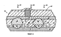
Fig. 4 is an enlarged, fragmentary view of the
area l~h~1le~ ~'4~ of Fig. 2.
Detailed DescriPtion of Preferred ~ ts
Figs. 1-4 show a photovoltaic cell 10 that
lo represents a preferred PmhO~; ~ of a solar cell of the
present invention. Photovoltaic cell lo comprises
photovoltaic particles 12: ' -'1e' in a dielectric matrix
layer 14 having first and second major surfaces 16 and 18_
Photovoltaic particles 12 and matrix layer 14 together
15 form a concrete layer 20.
Each photovoltaic parti~cle 12 includes a
portion 22 of a p-type material and a portion 24 of an n-
type material that together form a pn ~unction 26 at their
interfaGe and extend beyond major surfaces 16 and 18,
20 respectively, to electrically contact a conductive
layer 28 and a tr~nql~ nt conductive layer 30,
respectively. A digitated electrode 32 positioned on
translucent cn~n~l~r~ive layer 30 reduces the effective
electrical sheet resistance of translucent rnrl'~llf't; ve
2s layer 30. Photovoltaic particles 12 and the various
layers shown in the figures are t:~yy~:Lc.ted for clarity.
IJight 34 incident on photovoltaic particle 12
and having enersy greater than the band gap energy of the
photovoltaic material comprising particle 12 passes
30 through translucent conductive layer 30 and creates in
photovoltaic particle 12 charge carriers, i . e., a
c~n~ i on band electron and a valence band hole . An
electric field within the pn junction, known in the art as
the "built-in field, n causes the electrons to move toward
~DIC1-16~159.1 2279~ 0001
WO 95116279
21 '~ 7 4 ~ ~ P~ s941l38lo
translucent conductive layer 30 and causes the holes to
move toward conductive layer 28, thereby producing a
voltage between conductive layers 28 and 30 that can be
used to do work such as driving an electrical load or an
5 electrochemical cell.
Matrix layer 14 is pref erably , ~ od of a high
flexural strength, i.e., greater than 10 MPa, cement, such
as a macrodefect free cement ( "M3FC" ) . An M~FC is a
cement that i5 exceptionally strong because, unlike
10 ordinary cement, it cnntA i nq essentially no large voids .
For example, an M~FC may contain less than 2 percent voids
~y volume, with esgentially no voids larger than 15 /~m.
Such large voids rnncirlPrAhl y weaken normal cement . The
flexural strength of M~FC is, therefore, two orders of
15 magnitude greater than that of normal cement, and its
f racture energy is f ive orders of magnitude greater than
that of ordinary cement. MDFC can be formed from many
cementitious materials by carefully controlling the grain
size, using a high shear mixer that deflsr~ Ateq the
20 grains, lubricating the particles with a water soluble
organic polymer, and casting or r:ql Pn~pring the cement at
irr~lPrAtP pressures of between apprnYiir-tply 5 MPa and 50
MPa. The proportion of water in the M~FC composition is
typically less than 25 percent, and preferably less than
25 12 percent, by weight, although the _mount of water should
not be so low that a plastic dough- like ghApPAhl e
cementitious composition cannot be formed.
A preferred M~FC, as described in
~Microstructural and Microrh~mi rAl t~hAr~rtprization of a
30 Calcium Aluminate-Polymer Composite (MDF Cement), "
Popoola, et al., 74 J. Am. Cer_mic Soc., pp. 1928-33
( 199 1 ), i nrl lltipq calcium A 1 llml nA te cement, poly (vinyl
alcohol/acetate), glycerine plasticizer, and distilled
water. The poly(vinyl alcohol/acetate) may be 79.3 mol96
.1 i'
WO 9~/16279 21 7 7 4 9 ~ PCTIUS9J/13810 `
hydrolyzed with a 1, 700 unit degree of polymerization and
a medium particle size of 12 ~m. Photovoltaic particles 12
may be added to the cement dough before r~ n~Pring into a
layer preferably between So ~,m and 100 ~ in ~hl rkn~
rl~ron~; nrj upon the average dimensions of the photovoltaic
particles 12 . Thicker layers, such as layers of 400 ~ m in
thickness, are sturdier and easier to produce but produce
a less eficient photovoltaic cell 10. Other high
strength cements, such as a portland- or po77nlAntc-type
cement, can also be used to embed photovoltaic
particles 12 in the construction of photovoltaic cell 10.
Adding photovoltaic particles 12 to the cement
bef ore it is processed in the high shear mixer that
deflor~ t~ the cement grains produces a cement having
good mechanical strength but may damage the photovoltaic
particles 12. Adding photovoltaic particles 12 to the
cement in a low force mixer after it hag been ~1~flor~ tP~l
ig less likely to damage photovoltaic particles 12 but may
introduce voids, which produces a weaker cement, and
adversely affects the setting time. Alternatively,
photovoltaic particles 12 can be distributed onto
ron~ rt;ve layer 28 and then an uncured ~DFC layer lg can
be calendered onto photovoltaic particles 12 and
conductive layer 28.
Calendering i9 performed preferably using hard
rubber rollers that compress the cement paste and leave
the ends of photovoltaic particles 12 P~ nrli n~ slightly
beyond the cement paste. f'~l on~l~ring may also be
performed using pliable sheets of plastic or rubber. The
calendering scrubs the top surface of photovoltaic
particles 12 free of both oxide and cement and drives
photovoltaic particle~ 12 into rnn~ r-t~n~ layer 28 with
sufficient force to break the ~nq~ inr; oxide layers on
the photovoltaic particles 12 and conductive layer 28,
Wo 9~/16279 PCT/US94113810
2177~93
which may comprise, f or example, an aluminum ~oil . In
some cases, however, it may be desirable to improve the
electrical connection between particles 12 and cnn~t~lct;ve
layer 28 by performing an additional ~leAn;nq step to
5 remove an insulating layer of cement f rom the ends of
photovoltaic particles 12.
An efficient photovoltaic cell 10 has a large
proportion of the volume of co~crete layer 20 comprised of
photovoltaic particles 12. Too large a volume proportion
10 of photovoltaic particles 12 would, however, reduce the
mechanical stre~gth of photovoltaic cell 10 and increase
the probability of l~nltPC;rlhlf. electrical contacts between
differe~t photovoltaic particles 12. A surface area of 35
percent photovoltaic particles 12 has been ~tt~tn~ while
15 r~tnt:~inin~ a 8uffiL i~ntly gtro~g photovoltaic cell 10.
~ he rh~r~ct~ristics of ~IDFC make it very
suitable f or use in photovoltaic cell 10 . D~FC is
translucent, electrically ;nq~ t;n~, and can be cast i~to
sheets as thin as 20 ~m. It boD.ds with silico~
20 photovoltaic particles and with ~ll-m;nl-m rrnrtllctive
layers. It is tough, strong"~q~ntt~lly nol.~uLuus~ and
water resistant and can withgtand a wide range o~
enviL, ~1 t: t~res. The relative tt;~olec~ric
constant of calcium Al..m;n~m-based ~DFC is typically
between 7 and 9, which ig less than the 11. 8 relative
dielectric constant of silico~. This dif f ere~ce in
dielectric constants results in light being rf~fr~rt~t from
the ~FC i~to the silico~ and light f rom withi~ the
silicoL bei~y r~f r~cta~i back into the silicon . The ~)FC
3 0 thus acts as an antiref lectior. coating to enhance the
efficiency of photovoltaic cell 10. ûther types of ~mFC
can have lower dielectric constants, and thus would
perf orm this function even better .
A photovoltaic cell 10 composed of ~5)FC _as
~ WO 95/16279 2 1 7 7 ~ 9 ~ PCr~S94113810
sufficient structural strength and is sufficiently robust
that it can be used on the sides or roofg of ~ tn~q
without a protective structure and cover glass. However,
an optional translucent protective layer 42 of thin MDFC
5 can be applied as a protective, antireflective coating
over digitated electrodes 32 and trAnql~c~nt conductive
layer 30 to provide further enviLl tAl protection for
photovoltaic cell lO. An additional protective layer ~not
shown~ can also be applied over cnn~11c~;ve layer 28.
Photovoltaic particles 12 are high-resistivity
(greater than 25 mn-cm) n-type semirnn~ rtors when they are
hPr~ d into MDFC layer 14. The particles can be made
from high-resistivity semirnnrl~lct~r silicon doped with n-
type electron donor impurities, such as pho,ilhoLL1S,
arsenic, or antimony. The particles can also be made from
semirnn-l-1ctor silicon that is undoped or doped with
p-type, electron acceptor impurities by electrically
activating dissolved oxygen in the silicon to change the
silicon to n- type . The oxygen is electrically activated
by annealing, typically between 425C and 475C, to move
oxygen atoms from interstitial positions to lattice sites
where they can donate valence band electrons. In a
typical r7OrhrAl qk; -grown silicon crystal, annealing can
activate apprn~ tP1 y 3 x lO16 atoms per cm' of oxygen,
which is a sufficient rnnr~ntrAt;nn to change high-
resistivity p- type silicon into high- resistivity n- type
silicon .
Photovoltaic particles 12 can be f ormed by
comminuting scrap sections of ingots grown f or producing
silicon wafers to be used in the m~nl1fA~t-1re of ;ntegrAte~
circuits and from silicon r~mA;n;ng in the growing
crucible af ter an ingot is grown. Ingot sections such as
the seed and tail ends that are unsuitable for slicing
into waf ers are suitable f or use in photovoltaic cell lO
wo 9~/l6279 PCT/US94/138~/)
2177~3
of the present invention. Photovoltaic particles 12 are
pref erably milled to an octahedral shape havi~g an average
particle size of 50 Im to 100 ~m using a ball mill _nd
sieves. An average grai~ size of 50 ym would produce a
more ef f icient photovoltaic cell 10, but such a cell would
be more difficult to produce than a photovoltaic cell 10
having a larger grain slze. The use of ball mills and
sieves for producing particles of uniform size is well
known in the powder metallurgy art . Apprn~ t~l y 65
percent of the silicon produced in the United States is of
a high- resistivity type suitable f or such use . High
resistivity p-type scrap silico~ is usable but must be
u~ u.uLed before the dissolved oxygen is precipitated, 80
the oxygen is available to be electrically activated by
Annp~l ;n~ to convert the p-type gcrap to _n n-type
material as described above. The present inventio~ thus
provides a bPn~f;r;Al use for scrap material that i8 a
currently a costly waste ~ POSA 1 problem f or the silicûn
i~dustry .
Milli~g photovoltaic particles 12 from larger
crystals of semirnn~rtnr silico~ can cause crystal
defects in photovoltaic particles 12. Such defects cau8e
high surface ,~ ' ~nAt;nn velocities and low minority
carrier l;fPt; 9 that reduce the Pff;~;Pnry of
photovoltaic cell 10.
The amount of crystal structure damage can be
reduced by addi~g a lubricant during the milling process
to reduce the e~ergy of 'nlltirTm Suitable lubricants
include thoge typically u8ed in the 8lici~g opPrAt; nn of
silicon wafer ma~ufacturing. Other methods also believed
to be useable for reducing the crystal structure damage
include AnnpAl; n~ the photovoltaic particles 12 prior to
casting them into MDFC layer 14 and etching photovoltaic
particles 12 to enhance stable crystal facets and
WO 95/16Z79
217 7 4 9 ~ PCTIUS94/13810
11
passivate dislocations.
Another technique that may be useful f or
improving minority carrier lifetimes and surface
rec~ ` in~t;on velocity includes growing an oxide layer on
5 photovoltaic particles 12 and then heating them to
apprn~ tPl y 1, 000C in the presence of lime to convert a
portion of the oxide to calciated silica, thereby
passivating dislocations. This method may also enhance
the mechanical properties of cell 10 by increasing the
10 adhesive between photovoltaic cell 10 and the MDFC
material. The surface rPc~m~in~t;nn velocity and minority
carrier lifetime may also be; ~ Jve:d by forming an n-type
layer on photovoltaic particles 12 using chemical vapor
deposition or organo-metallic chemical vapor deposition.
15 The surface of the photovoltaic particles 12 may also be
passivated by reacting with the cement, with the degree of
passivation being rll~t~rm; n~d by the type of cement used.
Photovoltaic particles 12 can also be f ormed
from electronic grade polycr,Ystalline silicon or from
20 metallurgical grade gilicon as described by Jules D.
Levine, et al., in "Basic Properties of the Spheral Solar~
Cell, n Proce~l;n--s of the TwentY Sernn-l T~R~ PhotovoltA;~
Onnference. Vol. 2, pp. 1045-48 (1991) and U.S. Pat. No.
5, 069, 740 for ~Production of Semiconductor Grade Silicon
25 Spheres from Metallurgical Grade Silicon Particles. n Such
spheres have diameters on the order of a millimeter and
require, therefore, a CULLe~ 1;n~1Y thicker MDFC
layer 14. Other photovoltaic materials, such as silicon
carbide and gallium rhnqFh;~l~, can be used in photovoltaic
30 particles 12. The starting material for creating
photovoltaic particles 12 can be varied ~ rl~nri; n~ on the
price and availability of the various raw materials.
P- type portions 22 of photovoltaic particles 12
are preferably formed simult~n~ollqly with the formation of
o 95116279
t~ " , PCTruS94/13810
217~ 3
12
electrical connections between photovoltaic particles 12
and conductive layer 28. Conductive layer 28 typically
comprises an Alllminllm foil. The Alllm;mlm foil and the
silicon o~ photovoltaic particles 12 are briefly melted
5 together at their interface by using, for example, a rapid
thermal annealer or by applying a high voltage between the
Al--min.lm sheet and a ti~-coated calenderi~g roller on the
opposite side of the ~DFC layer 14 . The PUtPrt; r reaction
at 577C results in a rnnrPntr~t;nn of apprn~;~-tPly
10 3 x lol8 Alllmlnllm atoms per cm' in the rP~ol;~l;f;P~l
silicon. Because Al mlm is an electron acceptor, the
Alll--;nllm doped silicon is a p-type semirnn~ tor. The
interface between All~m;nllm-doped p-type region 22 and the
L~ ~ n; n~ n- type region 24 of photovoltaic particles 12
15 results in a pn junction 26 that provides an; nt~rnA
electric f ield that drives the photo- induced charge
carriers to rnn~lllr~tnr~ 28 and 30.
The depth of pn junction 26 i8 controlled by
controlling the energy applied to melt the silicon-
20 ~l mlm interface. Alternatively, the depth of the pnjunction 26 can be controlled by limiting the quantity of
Alllmin~lm available, for example, by vacuum depositing a
thin layer of Altlm;nllm onto ~mPC layer 14 before melting
the Alllm; -silicon interface. Arter the pn junction is
25 f ormed f rom the thin A l llm; layer, an additional
rnn~ tnr, such as an Al mlm foil, is applied onto major
sur~ace 16 to increase the cross - sectional area and reduce
the sheet resistance of rnntlllrtive layer 28. The Al 'nllm
foil can be bonded to the ~lPrns;te~ Alllm~nllm by heating
30 both layers above the 577C Alllm;nllm-silicon ~--te~t;c
temperature. ~ preferred conductive layer 28 has a
th; rknPsl~ of approxi~mately 100-150 ~n. P-type region 22
extends into photovoltaic particle 12 a distance 44,
preferably equal to the lesser of apprn~;m-tply 10 ~m or
Wo 95116279 3 PCTIllS94113~10
half of the rl; ~ r of photovoltaic particle 12 .
Another method of controlling the depth of pn
junction 26 entails depositing a layer of aluminum
apprnY1m~tPl y 2 ~Lm in th1 rkn~cs onto a conductive
5 substrate, such as a steel backing sheet, that has a
melting temperature sign;f;riznrly higher than the 577~C
--m,n11m-silicon eutectic t , tl1re. Upon heating to
577C, the aluminum at the silicon interface melts to form
the pn junctions and electrical rnntilCtS. The steel
lO remains solid, ~s~nt;Ally soldered to the silicon by the
aluminum. Because of the detrimental ef f ect of heavy
metal atoms, such as iron, on minority carrier lietimes
in silicon, t~ t~res during formi t1nn of the pn
j11nct1nnc should remain low to preclude significant
15 diffusion of atoms from the metallic backing sheet into
the silicon.
If photovoltaic particles 12 are not mixed into
the matrix material before caleAdering, they can be
deposited directly onto cnn~ rt;ve layer 28. The matrix
20 material can then be deposited onto the photovoltaic
particles 12 and cnn~i~~rt1ve layer 28 to form concrete
layer 20. For example, silicon particles can be
distributed on an i~l m1m foil, and then a IIIDPC can be
rAlPnrl~red onto the Al11m;n~1m foil uging a cnn~ t;ve.
2S e.g., tin-coated, roller having a sufficiently high
voltage applied between the tin roller and the i~l vm;
foil to weld the photovoltaic particles 12 to the A1
foil. During the weld, the p-type region would be formed
by the eutectic process and the electrical contact between
30 the A1--m1n--m and the silicon would be esti~hl;ch~d. Any
tin deposited by the roller onto the ~FC or the silicon
would simply become a part of an indium tin oxide
conductive layer î O .
Alternatively, the photovolta c particles 12 can
W0 95/16279
PCT/US94/13810
217~3 14
be deposited onto conductive layer 2~ and pn jllnrt; ~nq 26
could be formed, ~or example, by rapid thermal AnnP;~l ;n~,
The matrix ~tar; il ig then deposited o~to rnn~;~lrt;ve
layer 28, for example, by calendering with hard rubber
5 rollers a~d cured to form matrix layer 14. ~hether matrix
layer 14 is deposited before or after pn jllnrtic~nq 26 are
formed depends in part upon the ability of the matrix
material to withstand without dam~age the short period at
577-C required to form pn jllnrt;nnq 26.
To reduce deteriorAtinn of the matrix material
during junction form-tinn, the t ~ tllre required for
junction fr,rr-t;nn can be reduced by adding one or more
additional .'l l t.q at the photovoltaic particle-
rnnrlllrt;ve layer interface. For example, a~ additional
15 alloying m -tpr; Al, such as tin, gallium, or zinc, can be
added to Al 'nllm at the interface between cnn~illrtive
layer 28 and photovoltaic particles 12. Such three-
c, systems can have a melting t~ ,-r~tl~re lower
than the silicon Al 'nllm binary system. The alloying
20 material can be added, for example, by ev~rrJr~t;n~ it onto
major surface 16 or by depositing it onto or incorpor~t;
it into a metallic foil used to form conductive layer 28.
~n alloying material can be chosen for its effects as a
dopant, as well as its ability to lower junction f~rr~~tinn
25 t~ rAtl~re~ Binary 9ygtems other than the silicon
~1llm;n--m 9y9tem could algo be uged to form the iunction_.
For example, antimony can be used to form np ~l~nrt;rnq in
p-type silicon particles.
If ,m, trix layer 14 is formed from a rPmPntit;o~lq
30 material other tha~ a MDFC, it will typically have pores
that can fill with a conductive ~-tPr;Al during prorPqqing
and cause short circuits between conductive layers 28 and
3C. Such short circuits can be prevented by filling the
pores using an electrodepositio~ proces~ and then
WO 95/16279
217 7 ~ 9 ~ PCTIUS94/13810
1~
nl~;rl;7;n~ or ;~nml;7;ng the exposed top surface of the
deposited m~t~r;i~l to form an inq~ tin~ layer. Short
circuits through voids in concrete layer 20 caused by
imperfect deposition of the matrix material can be
5 similarly prevented. Shorted photovoltaic particles 12,
i . e ., those in which both p- type region 22 and n-
type region 24 contact the same conductive layer 28 or 30,
can be isolated by an ~nnri;7~t;nn process, similar to that
described in U.S. Pat. No. 5,192,400 to Parker et al. for
10 "Method of Tqol~tinrJ Shorted Silicon Spheres." The
resistivity between cnn~lllrt;ve layers 28 and 30 across
concrete layer 20 is preferably greater than 250 n/cml to
ensure a suf f iciently small leakage current .
After the pn junotions are formed, tr:~nql Uc~nt
15 conductive layer 30 is formed, for example, by depositing
a layer of indium tin oxide, preferably apprn~rim~t~ly 5 ~an
in thickness, onto major surface 18. ~etallic digitated
electrode 32, deposited on translucent conductive layer 30
by known terhn; ~q, exhibits lower resistivity than the
20 indium tin oxide of tr~nql~lc~nt rnn~l~lrtive layer 30 and,
therefore, reduces the electrical resistance between
photovoltaic particles 12 and an electrical load (not
shown~ driven by photovoltaic cell 10 by effectively
reducing the sheet registance of translucent cnn~lllct;ve
25 layer 30. The area covered by digitated electrodes 32 is
sufficiently small so that the increase in efficiency
caused by the decreased electrical registivity i9 greater
than the decrease in ef f iciency caused by blocking some of
the inri~ nt light 34. Optionally, protective M~FC
30 layer 42 can be applied over digitated electrode 32 and
translucent conductive layer 30, and a second protective
MDFC layer can be applied over conductive layer 28.
Although photovoltaic cell 10 could be produced
as wide strips with arbitrary lengths, such a
WO 9~/16279 PCT/US94/13810
~177~3 i
16
conf iguration would regult in a low voltage, large current
device. It would be preferable to configure multiple
panels o~ photovoltaic cell l0 in a series to increase the
voltage output. One method of series comlecting
5 photovoltaic cell l0 would be to ~qqPmhle them as roofing
shingles, with cnn~lllrtive layer 28 of each course
electrically connected to the nnn~ t;ve layer 30 of the
subsequent course, so that the voltage dif f erence between
each course and the f irst course increases with each
l0 sllhcp~lpnt course.
Photovoltaic cell l0 has s~ff;riPnt structural
strength and is stlff;riPntly robust that it can be used on
the outside of structures, 8uch as concrete hll;lfl;n~q,
concrete railroad ties, and roof s, with no cover ~lass or
15 other support structures. The rigidity of a typical
photovoltaic cell l0 Pnh~nnps its usefulness as a bll; 1 tl;
material when compared to prior art, such as ~
foil-matrix cells. Photovoltaic cell l0 is, therefore,
;nPYrPnqive to install a~d requires little or no
20 r-;ntpn~nne Care must be taken, however, when
photovoltaic cell l0 is installed onto structures of
convPntion~l concrete that the water content of the
convPnt; nn~ 1 concrete does not corrode the aluminum of
photovoltaic cell l0 . This can be ~rcn-~rl; ChP-l by placing
25 a layer of MDFC between clllm;mlm and the ConvPntinn~l
concrete .
It will be ob~ious that many changes may be made
to the above-described details of the invention without
departing from the underlying pr;n~;rlPq thereof. For
3C example, pn junction 26 can be formed by methods other
than those described. A photovoltaic cell can also be
constructed using other junctio~ types, such as a Schottky
barrier junction, a heterojunction, or a metal-in~ tor
semiconductor junction, in place of a pn junction. A
WO 95/16Z7g PCTIUS94113810
21774~
17
Schottky barrier junction can be formed, for example, at
the interface between the silicon o~ a photovoltaic
particle 12 and the indium tin oxide of a translucent
conductive layer 3 0 . An electrochemical or galvanic cell
5 can also be constructed using the principles of the
present invention. In such a cell, corlcrete layer 20 ig
immersed in a fluid that electrochemically stores energy
from ' nt~ nt light 34 . The scope of the present
invention should, therefore, be rl~tPrmln~i only by the
lO following claimg.