Note: Descriptions are shown in the official language in which they were submitted.
._ 2177~o s
(a) TITLE OF THE INVENTION
METHOD OF MAKING A PRINTED CIRCUIT BOARD
(b) TECHNICAL FIELD TO WHICH THE INVENTION RELATES
This invention relates to a method of making a printed
circuit board of the plate through-hole type, and in
particular to a method using board of the paper phenolic
material type.
(c) BACKGROUND ART
Plate through-hole (PTH) boards have conductive circuit
elements which are formed on both sides and are interconnected
by holes which are drilled through the board from a conductive
element on one side to an opposed element on the other side,
the holes having conductive metal plated therethrough.
In earlier published application W093/26145, a method of
making PTH boards using electroless plating was disclosed and
claimed. While the general method was suitable for use on a
wide range of substrates, it had not been possible to use the
most widely-used substrate, namely, laminated paper which is
bonded with phenolic resins, referred to as "paper phenolic
materials", because prolonged exposure to the hot alkaline
copper plating solutions required caused breakdown of the
substrate, and because such materials contained traces of
antimony, which can poison a copper-plating bath and render it
ineffective.
(d) DESCRIPTION OF THE INVENTION
By a first broad aspect of this invention, a method is
provided for making a plate through-hole printed circuit
board, comprising the steps of forming conductive circuit
elements on two opposed faces of a paper phenolic-containing
substrate, coating the substrate and the conductive circuit
elements with a de-sensitising material, forming holes through
the substrate, each hole passing through a circuit element on
each of the opposed faces of the board, treating the board to
render the substrate which is exposed in the holes receptive
to the action of a metallic plating solution, removing the de-
sensitising material, printing an acid-resist mask onto both
._ 2~~~~as
2
faces of the board, the mask leaving exposed only a small area
of the board surrounding each hole therethrough, and treating
the board with an electroless nickel-plating solution to
deposit nickel in the holes to the desired thickness to
provide an electrical connection through each hole between two
opposed conductive circuit elements.
By a second broad aspect of this invention, a method is
provided for making a printed circuit board, the method
comprising the following steps performed in the order given,
forming conductive circuit elements on two opposed faces of a
non-conductive substrate, coating the substrate and the
circuit elements with a desensitizing material, forming holes
through the substrate, each hole passing through a circuit
element on each of the opposed faces of the board, treating
the holes to render the walls of the holes receptive to
plating, removing the de-sensitizing material, and plating the
circuit elements and the walls of the holes with a first
plating solution such that a starter layer of two microns in
thickness is created upon the circuit elements and upon the
walls of the holes, and thereafter plating upon the starter
layer using an electroless nickel-plating solution.
By a first variant of the first and second aspects of
this invention, the de-sensitising material is a plating
resist coating material.
By a second variant of the first and second aspects of
this invention, and/or a variant thereof, the plating solution
is a non-homogeneous plating solution.
By a third variant of the f first and second aspects of
this invention, and/or variants thereof, the fourth step
comprises deposit of a catalytic material on the exposed
substrate.
By an alternative fourth variant of the first and second
aspects of this invention, and/or variants thereof, the fourth
step comprises subjecting the board to the following treat-
3 217~7o s
menu, namely, cleaning, sensitization, and acceleration in an
alkaline accelerator.
By a fifth variant of the first and second aspects of
this invention, and/or variants thereof, the first step
comprises applying an etch resist to the faces of a copper
clad laminate in a positive image of the circuitry, etching
away the exposed copper, and stripping away the etch resist.
By a sixth variant of the first and second aspects of
this invention, and/or variants thereof, the holes are formed
by punching.
By a third aspect of this invention, a method is provided
for making a printed circuit board, the method comprising the
following steps, performed in the order given forming
conductive circuit elements on two opposed faces of a non-
conductive substrate, coating the substrate and the circuit
elements with a de-sensitizing material, forming holes through
the substrate, each hole passing through a circuit element on
each of the two opposed faces of the board, subjecting the
board to the following treatments, namely, cleaning, sensi-
tizing, and acceleration in an alkaline accelerator, wherein
the de-sensitising material is removed from the board, and
plating the circuit elements and the walls of the holes with
a first plating solution such that a starter layer of two
microns in thickness is created upon the circuit elements and
the walls of the holes, and thereafter plating upon the
starter layer using an electroless nickel-plating solution.
Preferably, the de-sensitising material is a plating
resist coating material. The metallic plating solution is
preferably a non-homogeneous plating solution, which will only
plate onto areas which are sensitised or are treated to render
them receptive to the plating. Such sensitising typically
deposits a catalyst onto a cleaned and micro-etched surface to
initiate the deposition of metal from its solution.
In comparison with conventionally-produced boards, boards
which are produced by the methods of aspects of the invention
217770 8
4
are consistent in quality, and in uniformity of plating
through the holes. Since metal is not built-up equally over
the whole board during plating, but is concentrated on the
holes, the initial metal coating on the substrate can be
selected to be the design conductor thickness, thus ensuring
that all tracks meet the design specification. This is very
important in controlling the impedance of high frequency
circuits. The use of a single, electroless plating operation
before imaging ensures that no voids are present which might
give rise to out-gassing, and contamination cannot occur.
Further, although plating in the holes may not proceed
uniformly initially, because of the variation in the surface
smoothness in the drilled hole, or the, preferably, punched
hole, the resultant lack of smoothness in the surface of the
plated metal through the hole is advantageous in providing a
key for the solder in the subsequent use of the board.
The imaging of the conductive tracks is carried out
before the holes are drilled or punched, and involves the
formation of a positive resist image. This means that screen
printing of an alkali-strippable resist can be used. This is
not only a very low-cost operation, but requires only treat
ment in an alkaline solution to remove the resist, preferably
the alkaline accelerator bath which is used after sensitising.
Such treatment does not give rise to difficulties in waste
treatment, requiring no organic solvents.
The methods of aspects of the invention use only one
plating bath, thereby reducing cost and the problems which are
associated with treatment of waste from the plating stage.
Capital costs and running costs are substantially smaller than
with the conventional method. Control of the plating method
is simple and a high degree of precision in achieving design
plating thicknesses can be expected.
r~
2177708
Benefits arise from the use of electroless nickel-plating
solutions to deposit conductive metal in the holes. Firstly,
plating rates are very much higher than for copper solutions,
typically 25 ~m/hr, so that a satisfactory thickness of metal
5 can be built up in a much shorter time. Secondly, since
nickel does not tarnish in the way that copper does, it is no
longer necessary to coat the exposed metal on the board with
solder. This is conventionally done in a hot-air levelling
method, involving dipping the board into a bath of solder and
then removing excess solder and levelling by means of a jet of
hot air. This method is costly and potentially dangerous, and
can give rise to health risks due to metal vapour emissions.
Thirdly, electroless nickel-plating does not require the
presence of the formaldehyde which is required for copper
plating. Since formaldehyde is carcinogenic, its avoidance is
very desirable. Boards whose through-holes are plated with
nickel in accordance with the methods of aspects of the
invention have been found to meet the highest quality
standards, rendering them suitable for use in space and
aerospace applications, while production costs are comparable
to conventional standard production boards. The acid plating
bath which is used in the electroless deposition of nickel
does not attack paper phenolic materials, thus opening up such
materials to high quality electroless through-hole plating.
(e) DESCRIPTION OF THE DRAWINGS
In the accompanying drawings,
Figures 1 to 4 diagrammatic sectional views through a
board illustrating stages in a manufacturing methods according
to aspects of the present invention.
(f) AT LEAST ONE MODE FOR CARRYING OUT THE INVENTION
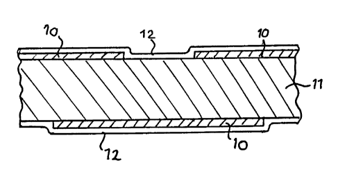
Referring to Figure 1, the method of one aspect of the
invention comprises as a first step the formation of the
conductive circuit elements 10 on each surface of the
substrate 11 by the conventional methods of forming a positive
resist image, for example, by silk screen printing, or
'3.
21~~~~ ~
6
photographically, and etching away the copper from the exposed
parts of the board. A uniform coating 12 of an alkali-soluble
plating resist is then applied to each surface of the board by
silk screen printing or dry film application as a de-
sensitising layer, and is cured, for example by the
application of U.V. light.
Holes 13 are then punched through the board and the de-
sensitising layer at the desired locations for
interconnections between opposed circuit elements 10, yielding
a configuration as shown in Figure 2. Treatment of the
exposed substrate in the holes to render it receptive to
electroless plating of nickel is then carried out in
conventional manner, with initial cleaning, micro-etching and
sensitising with any of the known electroless preparatory
systems, for example, the materials sold by MacDermid GB Ltd
under reference 9027. The next stage in preparation is
treatment by caustic soda as an accelerator, and this also has
the effect of stripping-off the de-sensitising resist layer
12.
A mask 14 of acid-resist is then printed on each face of
the board, leaving only a small area (2mm wide) around each
hole exposed, as shown in Figure 3. Since the only area of
the board which is prepared for plating of nickel is the
exposed surface within and around the holes 13, treatment of
the board in a strong electroless nickel-plating solution,
e.g., those sold by MacDermid GB Ltd under the trade-marks
ELNIC 105TM or ELNIC 110TM for one hour, builds up nickel to
the desired thickness in and around the holes only. This
leaves the configuration illustrated in Figure 4. It is
observed that the thickness of nickel 15 through the holes is
generally uniform, and consistent across the area of the
board, the plating of nickel being less subject to the faults
which can arise in the conventional electroplating techniques.
21~~~0 ~
Control of the electroless plating stage is conveniently
achieved as follows. The boards are suspended in a tank of
the plating solution, which is suitably circulated through an
overflow tank, where it can be filtered, so as to maintain a
constant volume in the plating tank. Air is bubbled through
the plating tank to agitate the solution and ensure adequate
mixing, and the supports for the boards are oscillated to
ensure that fresh solution is constantly passed through the
holes. The plating solution is replenished from a measured
supply by a dosing pump or pumps, which operate at a constant
predetermined rate, but which are controlled to switch on and
off repeatedly so as to run for a set percentage of the total
plating time. This is determined according to the amount of
nickel to be deposited.
c.