Note: Descriptions are shown in the official language in which they were submitted.
~~ ~~a~ 2
WO 95/20154 PCT/IB95/00033
1
10
FIELD OF ~=~TION
This invention relates to the field of
elactrochemical/gas analyzers, and more particularly to
the implementation of diagnostics in electrochemical/gas
analyzers.
$ACKGROUND SF T»~F~TION
Electrochemical/gas analysis systems are known having
sensor units for specific analysis tests selectively
installable in a multi-channel analysis system.
Electrical connections are made between the individual
sensor contacts and contacts on the analysis system.
Prior sensor electrode to analyzer system contacts
were extremely delicate and required time-consuming and
expensive hand assembly. Careless insertion or removal of
sensors into these connectors could easily result in
connector damage. In addition to low insertion-removal
cycle lifespans, these connectors frequently provided less
than optimal sensor to system signal reliability.
A major problem which prior art analysis systems fail
to address is the ease with which front-end electronics
with input impedances of several hundred million ohms can
be damaged by electrostatic discharge (ESDj which
occasionally occurs on insertion of static charged
sensors. Some sensors have plastic bodies prone to static
2177812
WO 95120154 PCT/IB95/00033
2
charge build-up, particularly when employed in low
humidity environments. A charged sensor brought into
contact with an analysis system contact can apply built-up
potential to the high impedance, front-end electronics,
thereby damaging them.
There is a need for simple and accurate diagnostic
testing of analysis system electronics including high
impedance front-end pre-amplifier circuitry and low
impedance back-end signal processing circuitry.
In order to test these elements, one prior art gas
analysis system provides a diagnostic tool which may be
referred to as an electrode simulator. In this prior art
analysis system, it is necessary to remove all of the
sensors from the system when it is suspected that either
a sensor or one channel of a multi-channel system is
malfunctioning. The sensor simulator, which is battery
powered, is installed in place of the sensors and is
electrically connected to the sensor contacts to provide
test signals to the analysis system through the same
contacts that connect the front-end and back-end
electronics.
Because all electrodes must be removed in order to
install the electrode simulator, time is consumed and
sensors which are not suspect are thereby subject to
foreign matter introduction, damage or loss. Further,
increased removal-insertion cycling decreases the life
expectancy both of the sensor and system contacts.
Finally, a discrete piece of test equipment such as the
electrode simulator is expensive to manufacture in small
quantities, requires separate maintenance, and must be
located and transported to the analyzer system site by
service personnel.
Another prior art approach to providing enhanced
testing of an electrochemical/gas analyzer system involves
2177812
WO 95/20154 PCT/IB95/00033
3
providing reed relays to selectively insert a test signal
to the high impedance front-end electronics in place of a
sensor signal. Contact testing cannot be achieved and
implementing reed relays requires additional space
proximate the front-end electronics.
$I~ARY OF THE INVENTION
An electrochemical/gas analyzer providing a rugged
contact system for removable sensors capable of
withstanding inexpert sensor insertion or removal,
providing protection for high impedance input electronics
against electrostatic discharge (ESD) damage, and
providing automatic connection of sensor front end
electronics to diagnostics upon sensor removal has been
invented.
The present electrochemical/gas analyzer provides
resilient electrical contacts as elongated contacting
stampings captured between a printed circuit board and a
sensor mating housing having flex in response to insertion
or removal of a sensor. Alignment of the sensor with
respect to an associated contact captured between the
housing and printed circuit board is not critical. The
contact stamping is easily fabricated according to known
stamping methods, and is capable of simple, fully
automated installation and retention between the printed
circuit board and housing of the present analyzer.
In the assembled printed circuit board and housing,
each contact stamping hasv~a remote partion which has a
spring loaded connection to a printed circuit board
contact that leads to ground or diagnostics. During
sensor installation, each sensor contact makes initial
physical and electrical contact with a.n arcuate (curved)
portion of the stamping while the remote portion remains
CA 02177812 2004-O1-13
4
in contact with the printed circuit board contact. As a
result, diagnostic circuitry, which may be disposed on the
circuit board, is connected through a remote portion
terminus to the sensor, and further to the signal
processing electronics. The diagnostic circuitry may
include a path to electrical ground through an output of a
voltage generator, or may provide a path to ground through
a switch. In either configuration, static potential built
up on the sensor body is drained to ground and the high
impedance front-end electronics are protected from ESD
damage.
When the sensor is fully installed, the remote
portion of the contact stamping is urged off the printed
circuit board, thus interrupting electrical connection
with the diagnostic circuitry and leaving the sensor
connected to the front end.
By merely removing a single sensor from the analyzer,
the remote portion electrically connects the diagnostic
circuitry to the signal processing electronics and allows
for fully automated diagnostic testing of the contact, of
the high impedance front-end electronics, and of the low
impedance back-end circuitry while other sensors remain
fully installed.
In accordance with an aspect of the present
invention, there is provided an electrochemical/gas
analyzer having plural installable constituent sensors and
providing diagnostic capability and electrostatic
discharge protection, comprising:
a housing
a mounting board disposed within said housing; and
a plurality of contact stampings captured between
said board and housing and electrically contacting input
CA 02177812 2004-O1-13
4a
signal circuitry, each of said plurality of contact
stampings further comprising a first portion in
interruptable electrical communication with diagnostic
circuitry providing a direct or low impedance path to
ground and a second portion for receiving a sensor contact
during sensor installation to provide electrical
connection between said sensor and said input signal
circuitry while maintaining connection to said diagnostic
circuitry and to interrupt said interruptable connection
when said sensor is fully installed.
In accordance with another aspect of the present
invention there is provided a blood gas analyzer having
plural installable constituent sensors and providing
diagnostic capability and electrostatic discharge
protection, comprising:
a housing;
a mounting board, said board disposed within said housing
and comprising:
signal processing circuitry, said signal processing
circuitry receiving inputs from plurality of input signal
contacts, and diagnostic circuitry, said diagnostic
circuitry providing inputs to a plurality of diagnostic
signal contacts and providing a direct or low impedance
path to ground, and a plurality of contact stampings each
having an input interface portion electrically connected
to a respective one of said plurality of input signal
contacts, each of said plurality of contact stampings
further having a remote portion in interruptable
electrical connection with a respective one of said
plurality of diagnostic signal contacts.
CA 02177812 2004-O1-13
4b
BRIEF DESCRIPTION OF THE DRAWINGS
These and other features, objects and benefits of the
present invention are more fully set forth below in the
detailed description of an illustrative embodiment and in
the accompanying drawing of which:
Fig. la is a schematic representation of an
electrochemical/gas analyzer according to the present
invention having a sensor installed therein;
Fig. Ib is the schematic representation of Fig. la in
IO which the sensor is shown removed:
I5
25
2177812
'"'""' WO 95120154 PCT/IB95100033
Fig. 2 is a perspective view of a measurement module
portion of the electrochemical/gas analyzer of Fig. la;
Fig. 3 is a perspective view of an interior region of
a housing of the analyzer of Fig. 2;
5 Fig. ~ is the perspective view of the housing of Fig.
3 having a printed circuit board installed therein;
Fig. 5 is a plan view of a bottom surface of the
printed circuit board of Fig. 4;
Fig. 6 is a plan view of a top surface of the printed
circuit board of Fig. 4;
Fig. 7a is a schematic view of analyzer diagnostic
circuitry according to the present invention;
Fig. 7b is a schematic view of a further embodiment
of analyzer diagnostic circuitry according to the present
invention;
Fig. 8a is a side, sectional view of the analyzer of
Fig. 2 showing a sensor installed;
Fig. 8b ie the side, sectional view of Fig. 8a
showing a sensor removed; and
Fig. 8c is the aids, sectional view of Fig. 8a
showing a s~nsor partially installed.
~,L~,QL~SCRIP'I'ION
A new and novel electrochemical/gas analyzer
configuration providing an analyzer capable of executing
comprehensive diagnostic testing, and of providing
electrostatic discharge damage protection for high
impedance front-end electronics, is disclosed.
With reference to Fig. la, improved diagnostic
testing over prior art analyzers is enabled in the present
invention by providing test signals at a point A such that
contact stampings Z0, high impedance front-end electronics
22, and low impedance back-end signal processing circuitry
2177812
WO 95!20154 PCT/IB95100033
6
24 are all tested. Test signals can be provided from
diagnostic circuitry 26 in the form of a discrete DC
voltage or current, a repetitive series of DC step
voltages or currents (simulating a sensor response output
signal), though other variations may be used. In one
embodiment, the source of test signals can be a digital-
to-analog converter (DAC). Other embodiments can utilize
the outputs of DC voltage or current sources.
To enable the provision of test signals at the point
A for testing as described, the contact stampings 20 of
the present invention having a remote portion 3o are
advantageously utilized. The remote portion 30 is made up
of an arcuate portion 32, which extends through a housing
aperture and against which one or more sensor contacts 41
of an installed sensor 40 presses, and a remote portion
terminus 34. In Fig. la, such a sensor 40 is installed
within the analyzer and sensor contact 41 is electrically
connected with the contact stamping 20, thus lifting the
arcuate portion 32. This in turn raises remote portion
terminus 34, interrupting electrical connection between
the diagnostic circuitry 26 and the rest of the analyzer.
In Fig. ib, the sensor 40 is removed, thus allowing the
remote portion terminus 34 to electrically connect the
diagnostic circuitry 26 to the remainder of the analyzer.
Each contact 20 as described herein is manufactured
from resilient materials and undergoes limited motion as
a result of installation and removal of a sensor 40. As
a result, a rugged contact stamping 20 is provided,
capable of withstanding improper sensor 40 insertion and
having a high insertion-removal life cycle relative to
prior art sensor connector systems.
Another important benef it is provided through the use
of the contact stamping remote portion 30 as described.
'"~" WO 95120154 . PCT/IB95I00033
7
Sensors 40 employed in analogous electrochemical/gas
analyzers typically employ plastic as shell material, thus
soaking the sensors 40 susceptible to static potential
build-up. When sensors 40 are first installed within
these analyzers, a built-up electrostatic charge can
discharge into the high impedance, front-end electronics
22 which are prone to electrostatic discharge (ESD)
damage. However, in the present invention, the diagnostic
circuitry 26 provides a low impedance or direct path to
electrical ground in addition to providing the test
signals. Thus, when the sensor contact 41 of a statically
charged sensor 40 is initially brought into contact with
the contact stamping remote portion 30, the static
potential is dissipated through the diagnostic circuitry
26 to ground.
With reference now to Fig. 2, a measurement module
for the electrochemical/gas analyzer according to the
present invention, including the remote portion 30, is
illustrated. Typically, the analyzer of the present
2o invention will simultaneously test several aspects of a
medium, such as blood, introduced through consecutively
disposed sensors 40a-40g. Also provided within the
measurement module is at least one component 42 (only one
such component is shown within this figure) which provides
an electrical connection to the measured medium and a
sensor to measure the temperature of the medium being
tested.
To gain access to the sensors 40a-4og installed in
the analyzer front panel 10, a thermally insulating cover
48 is raised as shown. The cover 48 preferably has an
opaque window 50 of a thermally insulating material such
as glass or plastic. With the cover raised, installed
sensors 40a-4og are exposed. By urging a compressive
member 52 away from the sensors 40a-40g (to the right in
CA 02177812 2004-O1-13
8
Fig. 2), any one sensor 40 can be removed from an analyzer
housing 60, the latter being better illustrated in Figs. 3
and 4.
A source for the medium under test and a receptacle
into which the tested material flows are illustrated in
Fig. 2 schematically and are known in the art. The source
can be substituted with a number of reference materials,
depending on which aspects of the medium are being
analyzed. Such materials may include reference gases,
calibration materials, etc.
The interior of the measurement housing has a contact
housing 60 illustrated in Fig. 3. Contact stampings 20
are secured on a stamping retention face 62 by positioning
retention members 64 across the contact stampings 20, then
ultrasonically welding the retention members 64 to the
stamping retention face 62. Other means for adhering the
retention members 64 to the retention face 62 known in the
art may be employed such as gluing, snap-fitting, and
using screws or the like.
Once the contact stampings 20 are in place, a printed
circuit board 70 is installed within the housing 60, as
illustrated in Fig. 4. The printed circuit board 70
itself is best viewed in Figs. 5 and 6, wherein printed
circuit traces and discrete components have been omitted
for the sake of clarity. With reference firs to Fig. 5, a
printed circuit board bottom surface 72 has input signal
contacts 74 which correspond to the contact stampings 20
disposed within the housing 60 (see Fig. 3). When the
printed circuit board 70 is installed within the housing
60, raised portions 78 of the contact stampings 20 are
electrically and mechanically connected with the printed
circuit board input signal contacts 74, which in turn are
electrically connected to an input to the high impedance
front-end circuitry 22 which may be mounted on the board
WO 95/20154 217 7 812 p~,~~~00033
9
70 as in zone 71 (sae Fig. 6) or externally, which could
include access through a computer.
Tlae printed circuit board 70 also has terminus
apertures 7b through which the remote portion terminus 34
of the contact stamping remote portion 30 extends when the
printed circuit board 70 is installed within the housing
60. As view~d in Fig. 6, illustrating a circuit board top
surfape 75, proximate each terminal orifice 76 is a
respective diaqr~ostic signal contact 80 electrically
connected with the diagnostic circuitry 2b, also typically
on the board 70, or external.
As shown in Fig. 7a, th~ diagnostic signal contact 80
may communicate directly with an output 84 of a test
signal generator 82 which provides both test signals and
a path to ground. In an alternative embodiment, as shown
in Fig. 7b, the diagnostic signal contact 80 may
communicate with the output of a switch 90, the switch 90
having inputs 92, 94 from the test signal generator 82 and
from a path to ground 86.
The input signal contacts 74 .and the diagnostic
signal contacts 80 are typically formed of gold. The
contact sta~pings 20 are typically manufactured of
phosphor/bronze with a gold plating. Providing stampings
and contacts of the same or similar material minimizes. any
thermocouple affects which may be present with dissimilar
materials.
The relative positions of analyzer elements with a
sensor 40 installed and with a sensor 40 removed are best
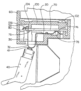
illustrated in Figs. 8a, 8b and 8c. In Fig. 8a, a cover
100 is shown in place, securing the printed circuit board
70 within the housing 60 by way of screws 102, though
other means for attaching the cover are employable. The
cover 100 has projections 104, each disposed proximate a
s terminus aperture 76, diagnostic signal pad 80, and remote
WO 95/20154 217 l 812 pCT/IB95100033
portion terminus 34. With the sensor 40 installed,
pressure is exerted by the sensor contact 41 against the
arcuate portion 32 of the remote portion 30, driving the
associated remote portion terminus 34 away from the
5 diagnostic signal contact 80, against a projection 104 and
interrupting electrical connection with the diagnostic
circuitry 26.
Without the cover projection 104, the remote portion
terminus 34 would describe an arc as the remote portion 30
10 is driven upwards by the sensor contact 41 and as the
sensor contact 41 is disengaged. As a result, without the
cover projection 104, the remote portion terminus 34 could
rest.against an edge of the terminus aperture 76 when the
sensor 40 is~...removed instead of returning to the
diagnostic signal contact 80. With the cover 100 in
place, the remote portion terminus 34 is guided, upwards
against the cover projection 104. The cover 100 also
provides a stop 106 for limiting the upward travel of the
remote portion 30 to prevent over-bending of the contact
20.
In Fig. 8b, the sensor 40 has bean removed, allowing
the remote portion terminus 34 to return to physical and
electrical connection with the diagnostic signal contact
80. It is in this position that diagnostic signals can be
conveyed to the analyzer processing electronics via the
contact stamping 20.
As shown in Fig. 8c, as a sensor contact 41 is
initially brought into contact with the arcuate portion 32
of the contact stamping remote portion 30, electrical
continuity is established between the sensor contact 41,
the contact stamping 20, and the diagnostic circuitry 26
via the diagnostic signal contact 80. As described with
respect to Figs. 7a and 7b, the ground path can be
provided either through the output of a low impedance
2177812
WO 95120154 PCT/IB95/00033
11
voltage source acting as a diagnostic signal generator 82,
or through a discrete path to ground 86.
Also visible in Figs. 8a, 8b, and 8c is the
electrical and physical connection between the raised
portions 78 of the contact stamping 20 and the input
signal contact 74 disposed on the bottom surface 72 of the
printed circuit board 70.
Although the invention has been shown and described
with respect to an illustrative embodiment thereof, it
should be understood by those skilled in the art that the
foregoing and various other changes, omissions and
additions in the form and detail thereof may be made
therein without departing from the spirit and scope of the
invention.