Note: Descriptions are shown in the official language in which they were submitted.
- ~177918
BC9-94-172
Video Receiver Display of Video Overlaying Menu
Background of the Invention
This invention relates to consumer use of what is here called the "television space". That is, the
use of video/audio signal streams such as in the past have been distributed by broadcast over radio
s frequency bands or by cable distribution, or made available from video recorder/player devices such as
cassette recorders or video disc player, or made available from direct, live sources such as cameras, game
systems or computers. Such video/audio signal streams, whether carrying analog or digitally encoded
h~roll,lalion, have come to represent a significant resource to most consumers for inrul,llalion and
entel l~i,llnenl.
Access to the television space has, in the past, been achieved by use of a television receiver. Then
came ch~nges in the methods of distribution, leading to the use of various set top devices such as cable
boxes for analog signal streams, recorder/players, game m~.hines home cameras, etc. As such devices
using the television space have proliferated, so also have the associated control devices. As television
space technology has a~p,ùacll~d what is pl~,s~ ly known as the "home theater", systems having as many
as seven or more con~tituent components which are connected one to another have become possible. In
such a systems of systems, several or even all of the constituent systems may have its own remote control
device, intt~.nded to enable a human observer to control the functionality of the respective con~titllent
system while avoiding the necessily of directly manipulating control available at the face of the system.
With the plûlirwalion of systems, a user is frequently faced with a proliferation of remote control devices.
At the same time as remote controls have been prolir~ ling, attempt to provide a "universal"
remote have been made. Such A~ ,.pt~ have resulted in remote controls having a manual interface, usually
in the form of buttons, which approaches or exceeds the limits of human usefi~lnes~ By way of example,
there are remote control devices offered with certain of the colll~,onenl systems for home theater use
which may have fifty or so separate (and se~Jalalely or jointly operable) buttons.
Such a proliferation of controls and proliferation of control functions results in an ~ n~geable
- ~177918
BC9-94- 172 2
situation for a consumer. Coordil-a~ control among a plurality of remote control devices and system
becollRs quickly difficult to the point of impossibility. Further, the user interfaces easily become
confused. It becollles difficult for a human observer to be certain of the response which may be achieved
by selecting and ach1~ting a particular button on a particular remote control.
The present invention proposes that these difficulties be resolved by providing, for the television
space and for other environlllt;llls presçnting similar problems of resource allocation and navigation, a
single remote control device which cooperates with a display controller and with control programs
~ ted by the display controller and an associated central proces~in~ unit (CPU). The remote control
device, in accoldallce with this invention, has access to the resources of the entire system with which it
is related. Further, the navigation among functions available and resource allocation is accomplished by
display of on-screen images which overlay or modify the images derived from the video/audio streams
entering the television space. This is accomplished with minim~l buttons to be ach~ted by the human
observer.
Summary of the Invention
S Wlth the above ~i~C~s~ion in mind, it is one purpose of this invention to assist a human observer
of progl~."",;~g made available in the television space, or similar displays found elsewhere, in making
selections of services or functions to be accessed through the system displaying the visual images so
derived. In accomplishing this purpose, the present invention overlays onto a menu display the visual
images currently being received and displayed as the principal progln."".;~-g By such a display, a user is
presented with a range of alternatives to viewing the present plincipal progln.,~ ;ng7 while there is still
displayed an image of that progl nl ~ ", .;~g as the user is advised of alternative choices.
Brief Description of the Drawings
Some of the purposes of the invention having been stated, others will appear as the description
proceeds, when taken in conne~;lion with the accolllp~ly;ng drawings, in which:
Figure 1 is a pe-~e~ilh~e view of one embodiment of the present invention which incl~des a
television receiver, a set top device, and a remote control;
~177918
BC9-94-172 3
Figure 2 is an enlarged pel ~pe.ili~re view of the remote control of Figure 1;
Figure 3 is a sçl~ic block diagram view of certain elements of the set top device of Figure 1;
Figure 4 is a sç~l ic block diagram view of certain elements of the set top device of Figures 1
and 3;
Figure 5 is a sc~ l ic block diagram view of certain elçm~nt~ of the set top device of Figures 1,
3 and 4;
Figure 6 is a pel specli~e view of another embodiment of the present invention which includes a
television receiver and a remote control;
Figure 7 is a pe, ~,ue~ e view of another embodiment of the present invention which includes a
o personal computer system and accessory input/output devices;
Figure 8 is an exploded perspective view of certain elements of the personal computer system of
Figure 7;
Figure 9 is a sçh~n ~tic block diagram view of certain elements of the personal computer system
of Figure 8;
Figure 10 is an illustration ofthe structure of a control program functioning with the systems of
Figures 1 through 9 in accordance with this invention;
Figure 11 is an illustration of the coding of a control program constructed using the structure
shown in Figure 10; and
Each of Figure 12 through Figure 18 is a view of the display screen of a television receiver of
20 Figures 1 or 6 or pe,~onal computer system of Figure 7 opel~ling in accordallce with this invention
Description of the Pr~re. . ~d Embodiment(s)
While the present invention will be described more fully hèreindner with rererence to the
acco,.lpa..yillg d-~wings, in which prere..ed embodiments of the present invention are shown, it is to be
understood at the outset ofthe description which follows that persons of skill in the applop,iate arts may
25 modify the inventions here described while still achieving the favorable results of these inventions.
Accordingly, the description which follows is to be understood as being a broad, te~ç~ing disclosure
dilecled to persons of skill in the approp,iate arts, and not as limiting upon the present inventions.
2177918
BC9-94-172 4
Before undertaking a detailed description of specific embo~im~nt~ of the present inventions, it is
believed useful to set forth some description of the en-viro~ s in which the inventions find utility.
In more cA~al1siv-e forms, the inventions are practiced using systems which have a video display
device, circuitry for driving a display of visual images by the video display device, a display controller, and
5 a remote control. In sil"pl~st form, the present inventions may be practiced through the use of a remote
control device and a display controller.
Vldeo display devices useful in the practice of the inventions here described are contemplated as
inr.l~ltlin~ glass envelope cathode ray tubes (CRTs) such as are co~v~ ;on~lly used in consumer electronics
systems such as television receivers and in pe, ~ollal computer systems, television projectors such as are
10 used in large ~ nce displays, liquid crystal displays (LCDs) similarly used, gas plasma displays, and
other flat panel displays. The listed types of devices are given as examples only, as it is contemplated that
the types of displays with which these inventions are useful will extend to include still other types of
display devices either not in common use or unknown at the time of writing this description, yet capable
of displaying visual images to a human obselvt;- in a manner similar to the displays presented by the listed
15 devices.
In any "~nce, the display will be coupled to circuitry capable of delivering to the video display
device video signals which drive the video display device to display such visual images. Such circuitry may
include analog or digital tuners for receiving video signal streams Ll~ ed or distributed at frequencies
which are outside direct sensing by the human observer and which carry data which is to generate, after
20 appropliale proce~Q;~, the visual displays. Specific examples of such circuitry will be given hereinaner.
However, it is C;Q.~ ted that the circuitry may include that typically found in a set top device used as
an accessoly to a television receiver, in a television receiver, in a personal computer system, or in other
types of consumer electronic systems.
~ldeo signal streams delivered to and through such circuitry may have a variety of characteristics.
25 The streams may be of co,l,pl~ssed signals, inwhich some il~",lalion has been conden~ed or co",plessed
by processing to f~cilit~te l,~ ion or storage. One set of such co",pression technologies are those
specified by the Motion Picture Engilleelillg Group (MPEG). In such event, the circuitry may include
provision for decol,lples~ion of the video signal stream. The streams may be of uncollll)ressed signals.
~177gl8
BC9-94-172 5
The streams may be of analog il~lllla~ion, such as conventional NTSC or PAL broadcast television
quality, or of digital inroll,lalion derived from ~ligiti7:in~ analog il~lmalion or by direct authorship. The
streams may be "live" in the sense of being ll~ ed and received and displayed concurrently with the
occurrence of the events depicted, or recorded. Distribution of the signals may be by broadcast or by
some broadband distribution method such as cable, optical fiber or the like.
In all embo~lim~tlt~ ofthese inventions to be here described, the video signal streams are delivered
to the video display device under the control of a display controller. The display controller, as described
more fully hereinafter, may be found in a number of di~relll enviro~ .s, now to be described.
One such envil~,n,l~l~l is provided by set top devices which, as contemplated by this invention,
may be in the form of cable tuner systems, such as are used in many homes to which video streams are
delivered by cable distribution netwolk~. Set top devices may have the capability of decoding satellite
ns~ sions~ or video signal streams distributed in digital form, with or without encl ~plion. They may
also be in the form of devices which include record/playback capability, such as VHS tape or videodisc.
They may also be in the form known as game m~ct~ines, of which the systems offered by Nintendo and
Sega are perhaps the best known. They may include back channel capability, so as to return a signal to a
distribution system, either directly over a distribution link or through an alternate channel such as a
conventional telephone line. A set top device may include some of all of the capabilities of the systems
briefly mentioned above, as well as others pelhaps not here set out in such detail.
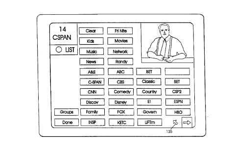
One such set top device is illustrated more specifically in Figure 1, where are shown a television
receiver 10, a remote control 20, and a set top device 30.
The television receiver 10 is prt;rt;l~bly a device of the type available to any consumer from any
supplier of television receivers, and will have a housing or cabinet 11 within which is all~1ged a video
display device 12. As described hereillabo~e, the display device 12 may take any one of a number of
forms. Also housed ~,vithin the housing or cabinet 1 1 is video reception circuitry (not shown in Figure 1 )
which is coupled to the video display device for receiving signals ~ led at frequencies which are
outside direct sensing by a human observer and for delivering to the video display device video signals
which drive the video display device to display visual images perceivable by the human observer. The
television receiver may be one configured to receive broadcast signals of NTSC or PAL standards or a
2177918
BC9-94-172 6
"cable ready" receiver which hllpl~n~ nte a design capable of directly receiving a larger number of çll~nnr l~
of analog signals such s may be distributed by a cable service provider. The television receiver may be one
configured to receive a digital data stream, although at the time of writing ofthis disclosure such sets are
not readily available colllll,ercially as a con~. . .er product. Details of circuitry for such receivers may be
5 found in any of a number of industry reference texts.
The video reception circuitry is contemplated as being capable of receiving signals which carry
analog il~lll~lion defining visual images to be lisplayed; digitally coded h~rollllalion dçfining such visual
images; or coll,plessed digitally coded il~llllaLion defining such visual images. Such signals as
contemplated as being lliln~...;lled by broadcast Ll~n~ ion or by cable tr~n~mi~sion or by satellite
10 tr~n~mi.e~ion or by ll~n~ c~ion through a telecollllll.mications network.
One form of remote control is shown in Figures 1 and 2 at 20. ~l~rt;l~bly, the control 20 is a three
axis remote control device usable at some rl;~l~nce of sep~alion from the television receiver 10. The
meaning of the phrase "three axis" will become more clear from discussion which follows later in this
description. The control 20 has a housing 21 sized to be held in the hand of a human observer of the
5 images displayed on the display device. The housing, while shown to be of a configuration particularly
intr.nded to lie comfortably in the hand of a user, may taken any configuration which is reasonably held.
The control 20 also has a manually ~ g~ble input device 22 mounted in the housing 21 for manipulation
by the human observer and control llt,~.~-..;llel circuitry (not visible in Figure 2) mounted in the housing
and coupled to the input device 22 for tr~n~n~ p at a frequency which is outside direct sensing by the
human observer colllllland signals coordil-aled in a pred~ellllilled manner to manipulation of the input
device 22 by the human observer. Such circuitry, while not shown, may be as used in other more
conventional hand held remote control devices such as are widely used by consumer electronic systems
such as television receivers and audio systems. As such, the circuitry may follow the te~ ings of
m~m~f~ctllrers of such devices.
The "three axis" characteristic of the input device can also be known as a "press to select"
d~ilelislic. Stated di~l~lllly (and as will become more clear as this description proceeds), the input
device may be m~nirll~ted from side to side, toward and away from the user's hand, and toward any point
around a circle centered on the device 22. If such actions were considered as if oriented to a compass
- ~177318
BC9-94-172 7
rose, side to side motion might be toward and away from East and West, while motion toward and away
from the user's hand might be toward and away from North and South. In this analysis, the device 22 is
capable of indicating movement toward any point of the three hundl ~d sixty degrees of the compass.
When so m~nip~ te1 the input device 22 will gen~lale signals which, in the contemplation ofthis
5 invention, will ul~ Ately give effect to movement of a cursor or pointer display ~lem~nt across the field
of view provided by the display device 12. Once such manipulation has positioned the pointer over an
applopliate portion of the visual images displayed (as will become more clear from discussion which
follows), then an action in(' c~ted by such an element may be selected by pl essing on the input device 22.
Thus movement to points of the compass rose (as discussed above) is movement on two axes, while
10 pl~ing on the input device 22 is movement along a third axis. It is the two axis movement for pointer
positioning and third axis movement for action selection which gives rise to the terminology "three axis"
remote control device.
The input device 22, while shown in one form, may take a variety of forms. In particular, the
device 22 is shown as what is here called a "wiggle stick". A wiggle stick, in the contemplation of this
15 invention, is an elongate member p*oted within the housing 21 of the remote control 20 and protruding
thererlolll. By suitable sensors, which may be strain gauge type devices or other ele~ ulllechanical
sensors, pressure exerted on the wiggle stick or physical movement thereof are tr~n.~duced into electrical
signals ;.~lic~ g manipulation by the human observer. Alternate forms of the input device 22 may be a
wobble plate (similar to the device found on commercially available game controllers used with game
20 " .~ es acce~ol ies for television receivers), a trackball, a mouse, or an inertial mouse. The latter two
forms of devices differ in that a mouse, as conventionally used with personal computer systems, rests upon
a surface over which it is moved by a user to gel~l~le signals e~ g movement of a cursor or pointer
display element across the field of view provided by a display device while an inertial mouse r~r~rel1ces
to a self co. .t~ d inertial pldl~llll and may be manipulated free of a surface, as in the air. Such a device
25 iS also known as an air mouse.
The remote control device 20 is coupled to the display controller (di~cllssed in greater detail later
in this description) in one of a variety of Illa,l,~el~. In the form illustrated in Figures 1 through 6, the input
device 20 is coupled by colllll~d ll~n ~ l circuitry mollnted in the housing 21 and coupled to the input
2177918
BC9-94-172 8
device 22 for L~ at a frequency which is outside direct sensing by the human observer col.~ and
signals cooldil~aled in a p-~d~Le--. i--ed manner to manipulation of the input device by the human observer
Such co ""~ signals, as is known to persons of skill in the arts related to other pointer control devices,
may be emitted by an infrared radiation emitter, a radio frequency emitter, or an ultrasonic emitter In
other forms, des i-il,ed hel~ler in connection with the pe. ~onal computer system of Figures 7 through
9, command signals may be transferred through an elongate flexible conductor
One form of set top device 30 is more particularly shown in Figures 3 through 5 and will be
described in some detail with rt;relence to those Figures However, it is to be recognized that the
particular device here des-i-ibed is only one of a number of varieties of such devices as alluded to
he~l~ove The illustrated embodiment plere-~bly has an analog multiplexer 31 through which many of
the signals flow among el~;-l-e--ls of the device 30 as illustrated in Figure 3 Signals re~çhing the analog
multiplexer 31 can arrive from an ~ntPnn~ or cable conne~ilion 32 through first or second tuners 34, 35
or a cable ;"1~ r;1ce 36 The cable interface may allow for decryption of securely encoded signal streams,
either on a single use ("Pay per view") or timed interval (subscription) basis The analog multiplexer 31
also serves as a conduit for signal streams from the output of an MPEG processor 38, the video processor
39, a video recoldil~g/playback device 40 such as a VHS video c~sette recorder/player or a videodisc
player, and auxiliary devices such as a camera (not shown) through a camera auxiliary port 42 or a game
machine (not shown) through a game auxiliary port 44
The video processor 39 is a central element of the set top device In addition to the elentP,nts
recited above, the processor 39 is operatively connected with system memory 45, an analog audio control
46, a microprocessor 48 functioning as a central processing unit or CPU, flash .lle-llo.y 49, an I/O
processor 50 in~ tlin~ an infrared receiver/blaster, an expansion bus 51, a cable or telephone modem 52,
and a Compact Disk (or CD) drive 54 Each of these e~ l s serves functions to be described more fully
heleina~ler.
The video processor 39 will be ~ ed in detail in the text addressing Figure 5 Suffice it to say
for now that the video processor 39 comprises the following functional blocks a memory refresher, a
video controller, a blitter graphical coprocessor, a CD drive controller, a digital signal processor (DSP)
sound coprocessor, and an ~;halOI to ~bi~la~e the access to the system ...e l-o-y between the six possible
~ 2177918
BC9-94-172 9
bus masters (the CPU, the blitter, the DSP, the memory refresher, the video controller, and the CD drive
controller). The arbitrator controls the çh~nging priorities of the devices, as described herein, and is in
electrical circuit comml-nication with all the devices within the video processor 39. For ~"~.lple, the CPU
48 has the lowest priority of all bus masters until an interrupt occurs. Thus, the arbitrator is in circuit
5 communication with both an interface to the CPU and an interrupt controller.
The CPU 48 has a SYSTEM bus associated with it. The SYSTEM bus incl~ldes a DATA bus,
ADDRESS bus, and CONTROL bus. The video processor 39 is the arbitrator for the system memory 45;
~I.e.~ru.e, the SYSTEM bus is modified to a SYSTEM' bus (comprising a DATA' bus, ADDRESS' bus,
and CONTROL' bus) by the video processor 39.
The system --t;nloly 45 comprises screen RAM, system RAM, and bootstrap ROM. The system
memory 45 will be discl~ssed in more detail in the text acco--.pa-.ying Figure 5.
The VO processor 50 interfaces the CPU 48 to numerous VO devices, such as the remote control
20, a keyboard, a tligiti7:~r, a printer, or a touchpad. In a prere..ed embodiment, the I/O processor is a
preprogl~.. ed MC68HC705C8 (helehldller "68HC705"), m~nllf~ct~1red by Motorola Corp, running at
2 MHz. The 68HC705 VO processor is interfaced to the CPU 48 by configuring the 68HC705 as a
pe.iphel~l device: (1) PA0-PA7 are connected to D0-D7 ofthe DATA bus; (2) PB7, PB1, and PB2 are
col~ne iled GPIO1 (a 32-byte address range decoded by the video processor 39), A1, and A2, respectively,
ofthe ADDRESS bus and CONTROL bus; and (3) PB3, PB4, and PB5 are connected to ADS, READY,
and WIR, respectively, of the CONTROL bus. Thus, the I/O processor is decoded to have four 16-bit
20 addlt;~s in VO space (referred to herein as AS0, AS2, AS4, and AS6). The I/O processor also interfaces
with al)plupli~le receiver circuitry which is able to detect and receive the signal packets emitted from the
remote control 20.
The program inside the 68HC705 i lt~;lr~ces to the CPU 48 as follows. The 68HC705 is designed
to attach directly to the processor bus and act as an VO port to the CPU 48. A pair of internal latches hold
25 data passing between each of the processors until the other is ready to receive it. Status bits to each
processor indicate the condition of the data latches. Each can tell if the previous data has been read and
if any new data is waiting to be read by checking the status bits.
2177918
BC9-94-172 1 0
The VO processor 50 implements the following functions: (1) a 50 ms timer, (2) a serial controller
link for input devices, (3) a system reset, and (4) a data/strobe/acknowledge (DSA) CD control
communic~tions link for the CD drive 54.
The 50 ms timer is i,~ ed using the watchdog timer of the 68HC705 VO processor. When
sthe watchdog timer expires, the VO processor interrupts the CPU 48 using analog interrupt 1 (A11) ofthe
video processor 39. The CPU 48 responds to this by reading the 16-bit I/O port AS0, described above,
which causes the video processor 48 to activate the VO processor, thereby causing a data ~ srer between
the CPU 48 and the VO processor.
Input devices are connected to the VO processor 50 via a serial controller link and controllers.
10The controllers l,an~ro",- the signalled movements of control devices into a format suitable for
on along the serial link. The controllers send data packets via the controller serial data link to
the system unit. The data packets differ dependillg on the type of IO device. Co-o,dinale t,vpe devices
(such as those with which the present invention is particularly concerned in~ ling a wiggle stick wobble
plate, mouse, joystick, etc.) have a di~lell~ data packet then a switch closure type of device (keyboard,
15digital joystick switch pad, etc). The controllers will include receivers approp,iate to any signals emitted
by a remote control device 20, such as infrared receivers, radio receivers, etc.The serial controller link consists ofthree (3) lines: a data receive line, a VCC (+5 VDC) line, and
a ground line. The 68HC705 i",pl~ments the data receive line of the controller serial link using the
PD01RDI pin. This pin is designed to be used as an interface to serial devices using the well known
20asynchronous format. A clocked synchronous format could be used in the alternative.
As alluded to hel~h,above, the CPU 48 gene~ales multiple buses: a DATA bus, ADDRESS bus,
and CONTROL bus, as are well known in the art. These three buses are collectively ,ere"ed to as the
SYSTEM bus. In the pre~ d embodiment, the CPU 48 is an 80376, m~mlf~ctllred by Intel Corp., 3065
Bowers Ave., Santa Clara, California, 95051. The 80376 is a variation of the well known 80386SX,
25which is well known in the art and also available from Intel Corp. The 80376 differs from the 80386SX
in that the 80376 st~rts up in 32-bit mode, rather than 16-bit mode. Sperific~lly~ the CR0 register is forced
to a 001 lH (0011 in he~r~deçim~l notation) state with bit 0 forced to a logical ONE, effectively making
the 376 operate in a 32-bit lll~;lllOly mode. Paging is enabled to allow virtual 386 operation.
-- 2177918
BC9-94-172 1 1
The present inventions contemplate that the CPU may access control programs stored, for
lp1~, in the set top device system memory 45 so as to be acces~ible to the processor, for controlling
the display of visual images by said video display device. As will be understood by persons of skill in the
design of progl~lll controlled digital devices, the processor accessi~-g such a control program will be
5 capable of loading the control program and opel~ g under the control ofthe control program so as to
accomplish the functions established by the author of the program. Such a control program may, for
example in this disclosure, cause the collllllalld receiver circuitry associated with or embedded in the I/O
processor 50 which receives command signals from the command ll;.n~",;ller circuitry of the remote
control 20 to derive from the rece*ed colll,llal1d signals image dile.;lh1g signals direcling modification of
10 visual images di~l~yed on the display device. Further, the control program will cause collllllalld processor
circuitry in the video processor 39 which is coupled to the coll~ d receiver circuitry and to the video
reception circuitry in the television receiver 10 to receive the image directing signals and modify the visual
images d;~layed on the device 12 as directed by m~nirll~tit~n of the remote control by a human observer.
In executing control programs, the systems here described will receive and store and deliver
15 digitally encoded data in lll~;lllOly devices and execute in a microprocessor coupled to the memory devices
digitally encoded control programs stored in the memory devices. The control programs will be effective
on ~Yecution by the microprocessor for modifying video signals in predetermined manners in response to
predetermined image direclil1g signals derived from manipulation of the remote control 20. Such
execution of a control program will include controlling microprocessor access to operational resources
20 of the television video display device by execution of an opelal;ng system program and/or controlling
modification of the video signals by execution of an application program. That is, the control exercised
is based upon both opel~ling system allocation of resoulce access and application program utilization of
~ccessed resources.
Additional circuitry associated with the set top device 30 is shown in Figure 4. Referring now to
25 Figure 4, the ~d-lition~l circuitry collll,lises four devices: a video digital-to-analog converter (video DAC)
55, an NTSC/PAL ("PAL" ler~lling to the well known European television signal standard) encoder 56,
an RF modulator 58, and an audio analog-to-digital converter/ digital-to-analog
converter/compressor/decolllplessor (ADC/DAC/CODEC) 59.
2177918
BC9-94-172 12
The video processor 39 has a number of functional blocks that will be more fully described in the
text accc ",~a"y",g Figure 5. It is sufficient for this point in the description to note that two such blocks
are a video controller 60 and a digital signal processor (DSP) 61.
The video controller 60 of the video processor 39 com1e~i~s to the external video DAC 55, which
5 converts ~ ePI~ bits of pixel ;,.ru,~ ion (six bits each of red, green, and blue) from the video controller
60 into an RGB signal, as is well known in the art. Each color channel (R, G, and B) of the video DAC
is imple."~,l1ed with an R2R resistor tree and a 2N2222 ~ ,.or. The RGB signal is converted to NTSC
composite video with the NTSC/PAL encoder 62. The NTSC/PAL encoder 62 accepts chroma clock,
HSYNC and VSYNC signals which are generated by the video controller 60 ofthe video processor 39,
and red, green, and blue video outputs which are generated by the video DAC 55, and generates a
composite video signal in the well known NTSC or ba~ebfln~ video format. In the alternative, the well
known PAL (European television signal standard) format can be generated. The composite video signal
is cc ~ P~led to an optional external composite video display device with a single female RCA type phono
jack as is well known in the art. In the pr~r~lled embodiment, the NTSC/PAL encoder 56 is an MC1377,
15 m5lnllfflt,~hlred by Motorola Corp.
An RF modulator 58 merges the composite video signal from the MC1377 with the left and right
audiû line out signals from an audio ADC/DAC/CODEC 59 onto a carrier frequency to generate an RF
video signal, in~lic~ted by RF Video, suitable for being directly input into the television receiver 10. To
generate the di~renl PAL (European television signal standard) and NTSC formats a di~re"l RF
20 modulator and crystal must be used. The RF video signal is col-ne~;led to external devices with a single
female Type F coaxial comle~;lor, as is well known in the art.
The audio ADC/DAC/CODEC 59 is linked to the DSP 61 with a serial link col~lll,ing tû the well
known Philips I2S protocol. The ADC/DAC/CODEC 59 converts analog data to digital data, and vice
versa, and co"~ sses and decolllpresses digital data. The ADC/DAC/CODEC 59 interfaces external
25 stereo analog data from optional micr~pholles to the video processor 39. The audio inputs are co~ec~ed
to external devices with a standard stereo 1/4" connector. The audio ADC/DAC/CODEC 59 also
interf~ces digital data from the video prûcessor to external devices by genelalillg left and right audio line
out signals. These signals are connected tû external devices, such as optional speakers with two female
`- 2177918
BC9-94-172 1 3
RCA phone jacks, as are well known in the art. As mentioned above, the audio line signals are also added
to the RF video signal.
In the plere"ed embodiment, the ADC/DAC/CODEC 59 is a CS4216, m~mlf~chlred by Crystal
Sem-con-luctor. The part contains microphone inputs, with proglal~lmable gain, as well as outputs with
s progl~l"",able ~ttçm~tors. Gain and ~tten~l~tion are both pro~lllllably controlled by the DSP 61.
In the alternative, the ADC/DAC/CODEC 59 can be replaced with a TDA1311 DAC
m~nllf~ct~lred by Philips. If this chip is used, the ADC and CODEC functions will not be available.
Referring now to Figures 3 through 5, the video processor 39 electronics are largely contained
within one massive custom logic chip, known as an ASIC (Application Specific Integrated Circuit). A
videv processor Illet;Ling the description herein may be purchased from MSU Ltd., 270 Upper 4th Street,
Witan Gate West, Central Milton Keynes, MK9 lDP F.ngl~n(l As illustrated in Figure 5, the video
plvcessvr co~ a plvce~or interface 68, a processor cache 69, a memory interface/refresh 70, a video
controller 60, an interrupt controller 71, a video blitter 72, a CD drive controller 74, a digital signal
processor (DSP) 61, and a DSP memory 76. The processor interface 68, the memory interface/refresh
70, and the video controller 60 are referred to collectively as the video/memory controller 78. The system
memory 45, central processing unit 48, and other devices lie outside the video processor 39.
The SYSTEM' bus electrically col~ne~ils the various devices to the system memory 45. Sharing
the SYSTEM' bus are six possible bus masters (in order from highest priority to lowest priority,
respectively): the memory refresh 70, the video controller 60, the CD drive controller 74, the DSP 61,
the blitter 72, and the CPU 48 (through the processor interface 68). Only one of the bus masters may
control the SYSTEM' bus (DATA' bus, ADDRESS' bus, and CONTROL' bus between the video
processor 39 and the system memory 45) at any one time.
The video/memory controller 78 controls the SYSTEM' bus, and provides the memory timing
signals (~ g" CAS, RAS, write enable, etc.) for "w",o,y devices ~tt~hed to the SYSTEM' bus, as is well
known in the art. It also requires memory cycles (video ~l~e~o~y cycles are le4uired to read video data
from system RAM; since video is gen~;laled in real time by this process, the video logic must have Ill~,llloly
access when video data is needed), and has effectively the highest priority on the SYSTEM' bus, as
mP.ntionP~d above. It sll~ppn~ls bus master operations during video lines for brief periods to fetch any video
-
2177918
BC9-94-172 14
display data, and to refresh dynamic RAM (DRAM). It also controls the interface with the CPU 48.
The DSP 61 is a simple, very high-speed processor for sound ~ylllhesis, operating at up to 33
million instructions per second (~Ps). It has access to the SYSTEM' bus via a DSP DMA controller (not
shown), which allows it to read and write bytes or words into system memory 45. These llallsrel~ occur
in short bursts, and are under DSP program control. The DSP 61 actually executes programs and stores
data in its own private high-speed memory 76.
The compact disk read DMA channel of the CD controller 74 allows the system to ll~1srer CD
read data into system memory 45 without any sonware overhead. It may ll~1~rer data dire~illy, it also
contains a CD block decoder.
o The interrupt controller 71 int~rf~t~s SiX internal interrupts to the CPU 48: video interrupt (highest
priority), analog interrupt 1 (All), analog interrupt 2 (A12), analog interrupt 3 (AI3), CD block decoder
interrupt, and DSP interrupt (lowest priority). The interrupt controller automatically clears an interrupt
when the CPU 48 pelrulllls the interrupt acknowledge cycle. A mask bit is available for each of the
interrupts.
The blitter 72 is a graphics processor for fast screen updates and animation, acting as a hal lw~re
graphics subroutine for the CPU 48 or DSP 61. It will become bus master through blitter program
operation, and may ILt;~rol~ own the SYSTEM' bus for considerable periods. However, its priority over
the CPU 48 is not absolute; it may be requested to give up the SYSTEM' bus to the CPU 48 when an
interrupt occurs. The CPU 48 is the lowest priority bus master at the system level; however, it has
complete control of the other l~dw~t;, Ihert;rùl e, the use of the SYSTEM' bus is entirely under CPU 48
program control.
The video processor 39 has four major blocks: a video/lllellloly controller 78, a compact disk
controller 74, a blitter graphics coprocessor 72, and a DSP audio coprocessor 61. The address space of
the CPU 48 is decoded to a number of eight-bit registers within the video processor 39. All internal
locations are on even address boundaries; word-wide VO reads and writes may be pelr~,lllled where
appropliate. In this particular embodiment, the byte-wide writes may not be pelrolllled on word-wide
registers and VO cycles may not be used to access odd addresses.
In addition to the above registers, the video processor 39 generates three spare general purpose
`-- 2177918
BC9-94-172 15
I/O decoder lines (GPIO1, GPIO2, and GPIO3) from the SYSTEM bus, each providing a 32-bit I/O
address range. The general purpose decoders may be used to provide three active low chip enables to
devices external to the video processor 39.
The video/~ oly controller 78 pelrulllls four functions: video timing, interrupt hQn-lling, video
5 display genel~lion, and memory configuration, refresh, and timing.
The video/memuly controller 78 has a flexible video timing generator that can be progl~ll.lled to
suit di~elenl TV standards and mûnitors up to a 640 by 480 VGA standard. The position of
sy~ ul~lion pulses, b~ in~, display area, active video (when the video processor 39 is fetching data
from memory) are progl~l..lled in clock cycles in the holizolll~l dimension and in line numbers in the
o vertical direction. Video timing is broken into two parts. Holizolllal timing is defined in terms of clock
cycles and is determined by a number of eleven-bit registers. Vertical timing is defined in terms of display
lines and is determined by a number of ten-bit registers.
There are nine holi~ûllLal registers: horizontal period, horizontal sync, horizontal blQnbing end,
horizontal blanking begin, horizontal display begin, horizontal display end, horizontal fetch begin,
15 horizontal fetch end, and holi~,ol-lal vertical sync. The value written to the horizontal period register
determines the h~ IJII~ line length in clock cycles. In one embodiment the line length is one greater than
the number written to the horizontal period register. The formula for the required number is: holi~,olllal
period = (line length x clock frequency) - one.
Thevaluewrittentotheholi~ull~lsyncregister~...,;nesthewidthofthehorizontal syncpulse.
20 The width of holi~onlal sync in clock cycles is given by the difference bt;lwt;~n the horizontal period
register and the holizonlal sync register. The formula for the required number is: horizontal sync =
horizontal period - (horizontal sync width x clock frequency). The horizontal blanking end register
determines when the holizolllal blanking ends and is the width of the back porch in clock cycles. The
horizontal bl~nking begin register determines where holi~onlal bl~nking begins. The formula for the
25 required number is: ho,i~"l~l blanl~ng begin = horizontal period - ((horizontal sync width + front porch
width) x clock frequency).
The ho,i~ullt~l display begin register specifies how soon video is generated after the trailing edge
of horizontal sync in clock cycles. If the horizontal display begin register is greater than the ho, izolllal
2177918
BC9-94-172 16
blanking end register the video/~ nloly controller 78 outputs the border color in-between. The value
written to this register should nollllally be chosen to put the picture in the middle of the television screen.
The formula for a register number to do this is: holi~ al display begin = (horizontal blanking end +
horizontal blanking begin - (active display width x clock frequency))/2.
s The holi~ll~l display end register specifies where the display ends and thelt;rolt; determines the
width of the video display in pixels. It should be programmed with the following number: holiGolllal
display end = hc,li~llt~l display begin + (number of pixels x clocks per pixel). If horizontal blanking begin
is greater than holiGolllal display end, then the border color will be output until blanking begins.
The horizontal fetch begin register dt;l~llllines where video fetches first start on the line. This
o should be progl~l.llled such that the sixteen byte pixel buffer has just been filled when the display begins.
In practice, this means that the value in the horizontal fetch begin register is given by the value in
ho~ l display begin less a con~ ull which dep~n-ls on the display mode. The table below conl&ins the
consla~ for various colllbh~alions of bits per pixel and clocks per pixel. For example, if four bits per
pixel and five clocks per pixel then the col1sldnl is 160. Likewise, if four bits per pixel and one clock per
S pixel, then the constant is 32. Note that if there are 16 bits per pixel and one clock per pixel, then no
constant is applicable.
Clocks per pixel
five ~our three two one
Bits per pixel four160 128 96 64 32
eight80 64 48 32 16
sixteen40 32 24 16 n/a
The holi~olllal fetch end register dt;l~llllines where video fetches end on the line. In principle,
this is the value in horizontal display end minus the above consl~lll. However, holi~.olllal fetch begin
should be rounded up so that holi~olllal fetch end register minus the holizolllal fetch begin register is a
25 multiple of the above con~lalll.
The horizontal vertical sync is identified as wider sync pulses occurring on a number of lines.
2177918
BC9-94-172 1 7
The width of these pulses is dele,lllined by the holi~on~al vertical sync register which should be
programmed as follows: horizontal vertical sync = holizolltal period - (vertical sync width x clock
frequency).
The video/ll-ellloly controller 78 also has a large number of vertical registers: the vertical
period register, the vertical sync register, the vertical blanking end register, the vertical blanking begin
register, the vertical display begin register, the vertical display end register, the video interrupt register
and the light pen registers. The vertical period register specifies the number of video lines per field.
The vertical sync register delel"~illes the number of lines on which vertical sync is generated. It should
be proglltlllllled as follows: vertical sync = vertical period - lines of vertical sync.
o The vertical blanking end register determines how many lines are blanked a~cer a vertical sync.
The vertical blal~Ling begin register dettlll~l-es how many lines are blanked before vertical sync. It
should be proglamnled as follows: vertical blal~ing begin = vertical sync - lines of bl~nking prior to
vertical sync.
The vertical display begin register determines the first line of active video. If this register is
S greater than the vertical blanking end register the lines in-belween show the border color. To position
the active area in the middle of the screen this register should be programmed as follows: vertical
display begin = (vertical b!anking end + vertical blanking begin - number of active lines)/2. The
vertical display end register determines the last line of active video. If this register is less than the
vertical blanking begin register the lines in-between will show the border color. To position the active
area in the middle of the screen this register should be pro~,l~llllled as follows: vertical display end =
(vertical bl~nking end + vertical blanking begin + number of active lines)/2.
The video h~lel I upt register determines the video line on which a video interrupt is gen~,. aled.
This interrupt may be enabled or disabled through the INT register. The interrupt occurs when the
video meçh~ni~m stops at the end of the display line. It may be used by the processor to change
display modes or to pelrorlll beam synchronous animation. The register may be reprogrammed within
a field to provide several interrupts per field.
The following table provides typical values for the above registers for the various display
formats shown. A~er loading the registers with the below values, the video timing generator is
~177918
BC9-94-172 18
enabled by setting the VIDEN bit in the register MODE2.
`- 2177918
BC9-94-172 1 9
50 Hz PAL 60 Hz Nl SC VGA
320 x 256, 320 x 220, 640 x 480,
8-bits 8-bits 8-bits
Clock frequency 22.17 MHZ 21.48 MHZ 25.17 MHZ
Ho,i~onlal period 1418 1363 790
Holizon~al sync 1314 1262 703
Ho"~onlal blankin~3 126 103 48
end
Ho"zonlal bl~nkin~, 1271 1232 688
begin
Horizontal display 378 348 48
begin
Horizontal display 1018 988 688
end
Horizontal fetch 346 316 32
be~in
Horizontal fetch 986 956 672
end
Holizo"lal vertical 103 89 0
sync
Vertical period 312 262 525
Vertical sync 309 259 524
Vertical blanking 20 15 34
end
Vertical blanking 307 257 514
begin
Vertical display 35 26 34
begin
Vertical display enc, 291 246 514
., 2177918
BC9-94-172 2 0
The video/memory controller 78 has three color resolutions available: four bits per pixel, eight
bits per pixel, and 16 bits per pixel. In four- and eight-bit modes, the pixel is a logical color that
indexes an 18-bit physical color stored in the palette. In 16-bit mode, the pixel is a physical color in
which bits zero to four are blue, bits five to ten are green and bits 11 to 15 are red. Because there are
5 SiX bits of green but only five bits of blue and red, the least significant bits of blue and red output from
the chip are always logical ZERO in 16-bit mode. The border color is a 16-bit register which is
displayed as a 16-bit pixel.
In eight-bit mode, the pixel addresses the whole 256 by 18 palette. In four-bit mode the pixel
addresses 16 entries from the palette in which case the top four bits ofthe addresses are supplied from
o the index register.
Two variations are available in eight-bit mode. In color hold mode if the pixel takes the value
zero, then the color of the previous pixel is displayed. This can be used to fill large areas of color
simply by setting the left most pixel.
In variable resolution mode, the most significant pixel determines whether the pixel is displayed
15 as one seven-bit pixel or two three-bit pixels. If the bit is clear, the pixel is displayed as one seven-bit
pixel; if the bit is set then bits zero to two are displayed first followed by bits four to six. In this case,
the two high resolution pixels address eight entries from the palette. The top five bits of the address
are supplied from the index register. Variable resolution mode is useful for displaying small regions of
high resolution text amid a lower resolution, but more colorful, background. This mode is not
20 available in one clock per pixel resolution.
In eight-bit mode any of the bits can be sacrificed and used for other purposes. For in~t~nre, a
bit could be used to identify "hot spots" for collision detection. Alternatively, bits could be used to
encode image "depth" so that one image can move in front of or behind another. To sacrifice a bit, the
same bit in a masked register is set and that bit will be replaced from the col-t;spol1ding bit in the index
25 register.
There are five widths of pixel: one clock, two clocks, three clocks, four clocks, and five
clocks. These correspond to dot clocks of around 24 MHZ, 12 MHZ, and 6 MHZ. The highest dot
clock may not be used with the 16 bits per pixel display mode. Two other colllbinalions: one clock 8-
2177918
BC9-94-172 2 1
bit and two clock 16-bit may only be used if 32-bit DRAM is fitted. If external hal Jwal e is fitted as
will be in the applications here described, the video processor 39 can gen-lock to an external video
source and mix (encrust) local video with external video on a pixel by pixel basis. This is significant
with regard to certain display to be generated in accordance with this invention as described more fully
5 heleill~ller.
The memory map of the screen is not tied to the video display width but is defined
independently. The base address of the screen can be anywhere in system lllellloly 45. The width of
the screen memory is the power of 2 from 128 to 2048 bytes. The height of the screen is a power of 2
from 32 K to 2 megabytes. Video addresses on the same line wrap within the smaller boundary. This
o ~ ge~ allows the screen to be placed within a larger virtual screen and panned and scrolled
within it.
Various registers control the video modes (ii~c~ ed above.
The video mode register controls the features listed above. Bits zero and one determine the
number of bits per pixel. Bits two and three dt:tt;llllil1e the pixel width in clock cycles. Bits four
15 through six determine the first break in the video address and hence the display width in bytes. Bits
seven through nine de~el llline the second break in the video address and hence the display height in
bytes. Bit ten turns the sync outputs into inputs which can reset the horizontal and vertical timers for
rapid locking to an external video source. Bit 11 controls encrustation, which is the overlaying of an
external video source using an external video multiplexer. The multiplexer is controlled by the "INC"
20 pin of the A/V/CD controller/coprocessor. Selected bits of the color are used to control encrustation.
Bit 12 controls border encrustation, which is the same as bit 11 but only applied to border colors. Bit
13 sets a variable resolution mode. Bit 14 sets the color hold mode, in which color 0 is replaced by
previous non-zero color in current scan line. Bit 15 enables Pixel clock widths of three and five based
on Bits 2, 3, and 15, as shown in the table below.
2177918
BC9-94-172 2 2
Bit 2 Bit 3 Bit 15 Pixel Clock
0 0 0 Four clock cycles/Pixel
0 1 Two ClockCycles/Pixel
0 1 0 One Clock Cycles/Pixel
0 Undefined
0 0 1 Three Clock Cycles/Pixel
0 1 Five Clock Cycles/Pixel
0 1 1 Undefined
Undefined
The video/l~lt;llloly controller 78 also has a pixel mask register and a palette index register. For
every bit set in the mast register, the coll~,onding bit in the pixel is replaced by the bit from the index
register. The upper bits in the index register form the high part of the palette address for 4-bit pixels. The
border color register is a 16-bit register that defines the border color. The color is displayed in the same
way as 16-bit pixels: bits zero to four are blue, bits five to ten are green, and bits 11 to 15 are red.
The video/lllelllol~ controller 78 also has two screen address registers that define the 24-bit base
address of the screen in system ~ ol~ 45. This is the address of the top left pixel on the screen.
The video/lll~llloly controller 78 also has an auxiliary video mode register MODE2 that provides
additional control over video and various test logic. Bit zero enables the light-pen registers so that the
IU 1~ and vertical counters can be read. Bit two enables the video timer, bits three and four determine
the refresh frequency with one indic~ting a refresh frequency of clocW128, two indicating a refresh
frequency of clock/256, and three indicating a refresh frequency of clockl512. Most DRAMs require a
refresh frequency of 64 KHz or above. The refresh controller waits until eight or more refresh cycles are
required then requests the SYSTE~ bus and does the required number of CAS before RAS cycles. When
bit six is set, the video mode is double buffered and can only change during bl~n~ing The CPU 48 sets
this bit for clean mode changes in split screen operation. Bit seven inverts the polarity of vertical sync.
Bit eight inverts the polarity of ho. i~o..lal sync and bit nine is not used.
217~918
BC9-94- 172 2 3
The palate is a 256 by 18 bit block of RAM at FlOOOOH - F103FFH. Each entry contains six bits
each of green, red, green and blue. Each entry extends across two words. The blue and green bits appear
in the high word. The red bits appear in the low word. Bits two through seven of the high word are blue;
bits 10 through 15 of the high are green and bits two through seven ofthe low word are red. To write
s to an entry in the palette, the CPU 48 must first write the red bits to the low word, then the green and blue
bits to the high word. The CPU 48 should only write to the palette during border or b!~nking or speckles
will appear on the video.
The cache 69 is not a cache in the sense that it plere~clles instructions for the CPU 48. Rather, the
cache 69 is a 512 x 16-bit static RAM located at F14000H to F143FFH that can be used by the CPU 48
o for ~uiabl~s, stack or pr~ code to speed up program execution. It comprises static RAM and is not
subject to page faults. Placing data, stack, or program code in the cache 62 allows quicker ~ccesses and
fewer page faults. In this embodiment, the cache is small and byte writes are not allowed to the cache
area. Interrupt service routines may not push bytes onto the stack.
Video/memory controller 78 supports six interrupt sources: video input interrupt, three analog
15 interrupts, CD block decoder interrupt, and a DSP 61 interrupt. The analog interrupts allow simple
analog-to-digital converters to be implçmented A monostable vibrator is implemented from a diode, a
~pa~tor, and a po~ ;u,.~le~ . The c~ r is discharged by vertical sync and begins cha~gillg at a rate
dçp~ le, ll on the potentiometer setting. When the voltage on the c~p~ritQr reaches the threshold of the
input to the video processor 39, an interrupt is generated. The processor can then read the vertical
20 counter to get a measure of how quickly the capacitor ch~ged, an hence the potentiometer setting.
The video/memory controller 78 also has an interrupt enable register allowing all six interrupts to
be indepeM(leMsly enabled or d;~' e ~ Writing a logical ONE to any bit in the interrupt acknowledge write
register clears the co~ onding interrupt. The interrupt read register reflects all pending interrupts.
The video/memory controller 78 decodes the 16 megabyte address range of the 80376 CPU 48
25 into the following memory map: eight megabytes of DRAMO (OH - 7~ H), seven ...eg~yles of
DRAMl (800000H - ~ H), 64 kilobytes of ROMO (FOOOOOH - FOFFFFH~, 64 K of internal memory
(FlOOOOH - FlFFFFH), and a 896 K block of ROMI (F20000H - ~ ~). The 64 kilobytes of internal
lllOly complises palette RAM, blitter registers, and DSP registers and memory. The palette address
2177918
BC9-94-172 24
range was stated above. The blitter registers extend from the range F10400H to F107FFH. The DSP
memory extends from F10800H to F18000H.
The on-board screen RAM and system RAM is 512 K of DRAM. The on-board DRAM
comprising the screen/system RAM may be either 16-bits or 32-bits wide. Suitable DRAM are the
TCS 14170BJ 256 kilobyte by 16-bit memory chip, m~mlf~ctllred by Toshiba. The size of the DRAM is
determined by the video processor 39 during reset but does not directly affect the CPU 48. Tn~tea~, it
allows the video/~ ;lll..ly controller 78 to operate more quickly leaving more bandwidth available to other
bus master candidates. Certain display and blitter modes are only possible with 32-bit memory. Two
banks of DRAM may be ~ .e~ as i~ led above. If small amounts of DRAM are att~he~, then they
will be repeated throughout the memory map shown above.
The bootstrap ROM is always 16 bits wide. The bootstrap ROM comprises two 27C512 erasable
progl~l"llable read-only memories, m~mlf~ctllred by numerous m~n~lf~ctllrers, thereby giving 128K of
bootstrap ROM. Following a reset, the one megabyte window from F20000H to ~ 1 co..l~ il-g
ROM and internal memory is repeated throughout the 16 lllega~yLe address range. This allows for a
15 variety of processors to boot with the video processor 39. The memory map above is adopted the first
time with the ",~",o,y type register is written to by the CPU 48. The video/memory controller 78
p~. r~., ...~ page mode cycles on the system memory 45 wherever possible. These are quicker than normal
memory cycles and occur if s~ccessive reads and writes are within the same page. The video/memory
controller 78 needs to know the number of columns in the DRAM, which is programmed in the memory
20 type register. In the memory type register, bit 0 and 1 determine the number of columns in the DRAM,
with 0 in~ic~ting 256 columns, 1 indicating 512, 2 indicating 1024, and 3 intlic~ting 2048.
The video/ll~ lloly controller 78 supports seven types of Ll~lsrt;l~: a normal DRAM cycle (4
clocks), a page mode DRAM cycle (two clocks), ROM cycles (6 clocks), internal lllellloly (2 clocks),
extemal I/O (6 clocks), interrupt acknowledge (2 clocks), and internal VO (2 clocks). The CPU 48 will
25 cycle in one more dock cyde than the actual ~ rer. Internal bus masters can cycle in the ~ srer time.
The video/memory controller 78 uses a crystal oscilldtor for a crystal that is the 2X (2 times speed)
dock for the CPU 48 and is a multiple ofthe television cl ror..i~ ce (chroma) subcarrier. This crystal
clock is buffered and output to the CPU 48. The same clock is put through a divide by two and this is
2177918
BC9-94-172 25
output as the main system clock. This clock is input to the video processor 39 through a separate pin.
The reason for olltr~lttin~ and inr~ltting the clock is so that the relative skew bt;lween the CPU 2X clock
and the main system clock, can be ~ lsted one way or the other by adding small delays to either path.
The crystal frequency also is divided by a progl~"lllable divider which can divide the crystal frequency
s by a number betwèen 1 and 15 and produce an output waveform with an even mark to space ratio. This
is used as the television color subcarrier.
The chroma divider register is a 4-bit register that defines the ratio ofthe television color subcarrier
(chroma) to the 2X crystal frequency. It should be programmed as follows: chroma = 2X crystal
frequency/chroma frequency - 1.
o The video/memory controller 78 also has a status register. If the status register bit O is set, the
video timing should be set up for PAL (European television signal standard). If bit O of the status register
is clear, then the video timing should be set up for NTSC. If bit 1 ofthe status register has been set, then
there has been a light-pen input in the current field. This bit is set by the light-pen and cleared by the
vertical sync.
The video/",t;",oly colltloll~ 78 can be put into a mode during reset a~er which it only responds
to two-word wide I/O locations and 64 K memory locations. The actual location of the VO locations is
de~ellllined by a chip select input so the locations can be detel"lh-ed externally. This "peephole" mode
allows the video processor 39 to occupy only small gaps in the VO and address memory map of the system
30.
The le~tel~ are 32-bits wide and must, lheler~JIe, be access~ as two 16-bit ~ccesses. To address
all the I/O registers within the video processor 39, the regular VO address of the required register is first
written to the lower word (a[1] low) then that register can be read or written at the upper word (a[1]
high). To address all the memory inside and outside the video processor 39 the 64K window can be
moved to any 64K boundary in the 16M address space normally decoded by the video/memory controller
2s 78 by writing to the bank register. The bank register is an eight-bit register providing the eight most
ific~nt bits when addr~ssing memory in peephole mode. For example, to access the palette, rollllelly
at FlOOOOH, the CPU 48 must write OFlH to the bank register and then read and write at the bottom of
the peephole location, determined by the external chip select.
~177918
BC9-94-172 26
The blitter 72 is a graphical coprocessor whose purpose is to pe~rullll graphics creation and
animation as fast as possible (limited by the memory bandwidth). It executes co~.. An~s written by the
CPU 48 and the DSP 61 into Ill~llloly. It can pe- rul ", ~1,;ll ~ ily long sequences of graphics operations
by reading new command sets from system memory 45 . While it is pel rul ll"ng graphics operations, the
5 blitter 72 beco",es a SYSTE~ bus master, and denies the CPU 48 any bus activity whatsoever. This is
reasonable because the blitter 72 is being used to pe,ru"n operations that the CPU 48 would otherwise
have p~,ru""ed, and is lhelerore sl,eeding up program operation. This also removes the need for any
synchronous control pro~,~.."";l~ for blitting operations and the need for any interrupt generation
l~dw~t; in the blitter 72. However, to allow real time prog,~ g of either of the other two processors
o (the DSP 61 and the compact disc DMA), the blitter 72 will suspend its operation and grant the SYSTE~
bus to the DSP 61 or the compact disc DMA r~ lc if they require a DMA L~ srer. It will also suspend
itself and give up the SYSTEMl bus to the CPU 48 if an interrupt occurs. During any of these 1, ~nsr~
the current op~l~liol1 is s~ ed but will restart when the interrupt signal becomes inactive or when the
DSP 61 DMA access completes.
The operation of the blitter 72 is best viewed as a simple program:
read command from memory
for n=O to outer_count
read p~ ~melers from memory
for m=O to inner_count
if SRCEN then read source from ",e",o,y
if DSTEN then read destin~tion from memory
write destin~tion to memory
next m
next n
The co"""~nds and operands are written to memory by either the CPU 48 or the DSP 61.
The blitter 72 has several registers in the video processor 39 I/O space: (1) two writable blitter
program address legi~tt;,~, which share the same VO address as two readable blitter destin~tion registers,
(2) a writable blitter co~ nd register, which shares the same I/O address as a first readable blitter source
address register, (3) a writable blitter control register, which shares the same I/O address as a second
readable blitter source address register, (4) a readable inner count register, (5) a first writable blitter
217~918
BC9-94- 172 2 7
diagnostics register, which shares the same I/O address as a readable blitter outer count register, (6) a
second writable blitter diagnostics register, which shares the same I/O address as a readable blitter status
register, and (7) a third writable blitter diagnostics register.
The blitter 72 may be operated in a variety of modes to pe-r,l-.. graphics and block move
op~l~liolls. The blitter 72 has an internal architecture divided into three largely separate blocks: the data
path, the address generator, and the seqll~nc~r. The data path co--lah-s three data registers: the source
data register, the destin~tion data register, and the pattern data register. The data path also co~-lah-s a
versatile co.,.pa,alor to allow intf!llig~nt blitting operations, and a logic function unit (LFU) to gene-~le
the output data.
o The address generator contains three address registers: these are the program address register
used to fetch blitter co.. ~nd~, and the source register and the destin~tion address registers. It also
contains an ~ill....elic logic unit (ALU) with an associated step register to update addresses, and a
mull;pl~".er to gelle.~le the output address.
The sequencer acts in software terms as the program that the blitter 72 runs, with two loops (an
15 inner loop and an outer loop) and a several procedures, as illustrated above with the short simple program.
The program is fixed, although various parts of its operation are conditional upon flags in the blitter
cGm.. al1d register and the loop counts are also part ofthe co.. ~n~
The data path colll~il s three data registers and two data manipulation blocks: the logic function
unit, which can combine the contents of the data registers in a number of useful ways to produce the
20 output data, and the co-,-p&,~tor, which can pc;.rO.... certain co~ ,~isons on the data to inhibit write
operations, and optionally stop blitter operation.
The data path can handle data of four sizes: 32-bit, 16-bit, 8-bit, and 4-bit. Long words (32-bits
wide) are used when p~.rO.., h~g fast block moves and fills. Pixels (4-, 8-, or 16-bits wide) may be
manipulated using all the blitter modes, such as line-drawing, multiple plane operations, character p~ ;"g,
25 etc.
The majority ofthe data path is 16-bits wide, which is the m~xim~m screen pixel size. However,
the source data register is 32-bits wide, and the top 16-bits of the source data register are used to produce
the top 16-bits of the data written in 32-bit mode, regardless of the mode of the logical function unit.
- 2177gl8
BC9-94-172 2 8
Thus, there are two 16-bit wide registers (pattern data and destin~tion data) and one 32-bit wide data
register (source data register). The source and destin~tion data registers are loaded from the source and
d~.stin~tion addresses in system memory 45 when the col,esponding read cycles are enabled in the inner
loop. However, all three data registers are loaded at the start of blitter operation with the pattern data,
s and this may be used as an additional source of data, either in producing the output data or in the
colllp~ulor. For example, the data in the pattern data register could be a mask, a pattern for writing, or
a lereLence value, for t;~alllple. The pattern data is loaded into both words of the source data register.
The logic function unit generates the output data, which is written to the clestin~tion in system
llællloly 45. It can pe~ru~m any logical colllb I~tion ofthe source and dçstin~tion register pixels. "Source
10 data pixels" may be selected from either of the source data register or the data pattern data register. The
LFU selects any of the four Boolean l,li,,~e,,,,s (A & B, A & B, A & B, and A & B) of the two sets of
input data from the data l~t~l~, and gel~lules the logical OR of the two selected minterms. This allows
any logical colllbindlion of input data; thus 16 functional possibilities exist.In 32-bit mode, the LFU will normally be set to produce source data, because it is only 16-bits
15 wide. The upper sixteen bits written during a long-word write are always derived from the top sixteen
bits of the source register.
The comp~utor can pelr~llll a variety of colllpalisons on the data in the source, destin~tion, and
pattern data ~ el~. If its co,~p~ on conditions are met, then it generates an inhibit signal. The inhibit
signal is used to inhibit a write operation, and optionally, to stop the blitting operation. The col"palulor
20 may also be used to provide a pixel plane effect, to give ~ spalelll colors, for collision detection and
system Ille,lloly 45 search operations, and as an aid to character pai"~ P
A multiple plane operation is supported by ~signing a plane number to every pixel. This mode
is only applicab'e to 4 and 8-bit pixels. In 8-bit pixel mode, two ofthe 8 bits (bits 6 &7) are used giving
two or four planes; in 4-bit (nibble) pixel mode, one ofthe 4 bits (bit 3 & bit 7 ofthe two-nibble byte) is
25 used giving two planes. The con~pal~or can produce an inhibit output if the plane number of the
de~tin~tion data is not equal to or greater than the plane number ofthe source data, or any co",binalion
of these. This means the data being written onto the screen can be masked by data already present in a
di~re,ll plane.
21 77918
BC9-94-172 2 9
The co~ )al~lor can produce and inhibit output if the entire source pixel is equal to or not equal
to the destin~tion pixel. This may be used, for ~ ll,ple, for searchillg, system Ille"loly 45 for a particular
value and, more i",po, L~lly, for desi~nAting a color to be ll~ spalenl and holding the ~ ale"l color
value in a data register. This applies to 16-, 8-, or 4-bit pixels.
The blitter 72 also has a colllpal~lor bit to pixel expansion mode operation. This col,lpal~lor
operation allows bit to pixel expansion of data, used, for eA~nple~ for character p~intin~ In this mode,
the comparator selects a bit of the source byte based on the value of the inner counter and inhibits the
write operation if this bit is a logical ZERO.
The blitter 72 makes provision for h~n~J~ p three pixel resolution modes. These are: 16-bit mode
o where each word corresponds to one pixel, 8-bit mode, where each byte colles~onds to one pixel, and
4-bit mode, where each byte collesponds to two pixels. In 8- and 16-bit pixel modes, the data path is
h~ndlin~ one pixel at a time, and operation is straight r~ d. In 4-bit pixel mode, however, only half
of the byte that is read from or written to system memory is the current pixel, Ihel~;rol-e, certain additional
requhelllenl~ are placed on the data path. In a 4-bit mode write operation, unçh~need destin~tion data
iS written to the halfofthe data byte that does not colle~ond to the current pixel. Thus, destin~tion reads
must always be enabled in 4-bit mode (set control bit DSTEN). This must be done because there is no
provision for writing less than one byte into main memory.
It is also possible that the source 4-bit pixel address and the destin~tion 4-bit pixel address point
in din`elèllt halves of the COI 1 t;~onding bytes of RAM. If this is the case, a shifter swaps the two halves
ofthe source data. In 4-bit mode, the two nibbles (half a byte; 4 bits) ofthe pattern byte should normally
be set to the same value. Note that the pixel with program in the blitter 72 does not have to match the
display width, and the most efficient way of moving large ~mounts of data is 32-bit mode. Recall that such
mode ll~1srel~ must be long-word aligned and the system must be fitted with 32-bit RAM.
The blitter 72 also has an address generator. The address generator col-laills three address
registers, an incre"le"l or step register, an address adder, and an address output multiplexer. The three
address l~el~ hold the source address, the de~ AIion address, and the program address. Each ofthese
le~i~lel~ is a 24-bit register allowil~g the blitter 72 to address up to 16 megabytes. In addition, the source
and destination address registers contain a nibble bit used in 4-bit pixel mode. The program address
2177918
BC9-94-172 30
register holds the address that the program is fetched from, and is incremented by one word each time a
memory cycle is performed using it. This register is always even, thus, bit O must always be a logical
ZERO.
The source and de~l;..nlion address l~k;l~ are updated after each cycle, and at other times, using
5 an adder that allows them considerable flexibility in the objects to which they refer. All source and
destin~tion address updates, may be pt-ro-ll,ed optionally on just the bottom 16 to 19 bits ofthe address
register. This means that the blitter 72 will then effectively operate in 64K, 128K, 256K, or 512K pages.
In this mode, if an address over~ows within a page, it will wrap and the overflow or underflow will be lost.
The blitter 72 also has an address adder, which is a 25-bit wide adder used to update addresses.
It allows either a con~ll value of .5, 1, or 2 or a variable stored in one of the step registers, to be added
to an address value. It can also subtract the same values. The 25th bit is the nibble part of the addresses,
as stated above. An ill~ lllt;lll of one pixel has a di~elel-t effect on the address depending on the current
setting of the screen resolution.
All address r~gi~ are updated ~lltom~ti~ y at the end ofthe appr~pliate memory cycles; source
15 read for the source of address register, and destin~tion write for destin~tion address register. Addresses
can be made to wrap vertically by using the SWRAP and DWRAP bits in the blitter co~ o~n(1~ and
horizontally by using the SLWRAP and DLWRAP bits in the blitter control register.
The address output multiplexer provides the external address to the system memory 45. It
provides three types of addresses: source address, destin~tion address, and the program address. These
20 are derived directly from the corresponding address registers.
When the blitter 72 is drawing lines, the address registers are used in a di~renl way than normal.
The destin~tion address register is used as the line draw address, and the source address register and the
step register are used as delta one and delta two respectively. During line drawing delta two is subtracted
from delta one, and the borrow output produced is used to d~;le---lille what is added to the destin~tion
25 address register. For further details, see the section on line drawing below.The blitter 72 also has a sequencer which controls the operation of the blitter 72. The flow of
control is best considered at two levels. There is an outer loop governing the overall flow of control and
an inner loop which pel~lllls the actual blitting or line drawing operation. The three sections within the
-
2177918
BC9-94-172 3 1
outer loop: the col.lllland read procedure, the pal~lllcler read procedure, and the inner loop.
The inner loop performs the actual blitting or line drawing operations. An inner loop cycle can
contain up to three memory cycles. These are a read from the source address, a read from the destinAtion
address, and a write to the de~ l ;Ol- address. All three cycles are optional. If the loop includes a source
5 read, or a source read and a destinAtion read, then the collll,al~lor inhibit ~llecl~An;~ is tested before the
cle~ l;on write occurs. This allows the write cycles to be bypassed when a colllp~lor inhibit condition
is met. When the colllp~lor inhibit conditions are met, it is possible to have the current operations cease
and control returned to the CPU 48. The program may then examine the address registers to determine
where the inhibit has occurred, so that collision detection may be pelrolmed. The CPU 48 may then
o d~t;- -. e wllt;lh~r to resume the operation or abort it. The inner loop pelrolllls operations until the inner
loop counter reaches zero. The inner loop counter is a 10-bit counter, so the inner loop can iterate any
number oftimes from 1 to 1024.
The blitter 72 makes provision for collision detection by allowing operation to stop when a
colllpalalor write inhibit occurs. When this happens, control returns to the CPU 48, which may then
15 examine the internal state of the blitter 72 to determine what has caused the collision. At this point, the
CPU 48 may choose to allow the blitter 72 to resume the operation it was pe,r~,r""ng, or may reset it back
to its idle state. Either a reset or a resume co...,--Al-~ must be issued before the blitter 72 may be used for
another opel ~lion. Note that while the blitter 72 is in the suspended state, a new value may be written to
the co..... .....-mal1d register, so that the collision stop --eclw-i~m may be disabled.
The pa-~---eler read procedure is a very straigl-lru-w~ld sequence that loads a new set of
parameters to the inner loop. It reads from menloly, in order, the inner loop counter value, the step
register values, and the pattern value, which is used to preset the data registers. The inner count
effectively beco...es the number oftimes the inner loop is ~Y~Ited The step registers are used for address
incle..~ and the pattern register is used for data manipulation.
The pz-~--eler read procedure is called as part of a command read procedure at the start of a
blitting operation and is also called if required by a blitting operation, as det~"",ned by the PARRD
control bit. EYtra pa-~."eler reads occur between passes through the inner loop to allow pa-~ lers to
be altered, thereby allowing operations such as irregular shape painting and run-length encoded data
~177918
BC9-94-172 32
deco",l,ression.
The co"~ d read procedure is used to start a new blitting operation. The blitter 72 starts in an
inactive reset state, which represents the normal inactive state ofthe blitter 72. From this state a co~ and
register write is pe~ro-lned to start the blitter 72, usually preceded by a write to the program address
5 register. A full set of operational pa~ ers is loaded from program count address which is auto-
incle...r;,.le-l, and control passes out ofthe con""alld read loop. When a blitting operation is complete,
a new co.. ~ 1 is read from the program count address and if this colllll,and leaves the blitter 72 in run
mode, then a new set of parameters is loaded and another operation is started. Other~,vise the blitter 72
enters its stopped state and returns the SYSTE~ bus to the CPU 48. The above mec.h~nicm allows the
10 blitter 72 to pe~ru"" &Ibi~l~ily long sequences of graphics comm~n-lc without requiring any processor
intervention. This is c,~llt;lllely useful because processor I/O write cycles are relatively slow in comparison
to blitter memory reads.
Normal operation of the outer loop starts on exit from the con""alld read loop. The parameter
read loop is then entered to read the first set of parameters and the inner loop is entered with the inner
5 counter being loaded to its initial value before the start of operation. The outer counter is then
decremented, and, if it is zero, the col"",alld read loop is entered. Then either or both of the source
address and destination address registered may be updated with the contents of the step register. The
pL~"~ler read loop may then be optionally entered to update various inner loop parameters, before the
inner loop is entered again. The two loops allow the blitter 72 to pe,ru,l" operations on with two-
20 tlim~ncion~l screen structures, with the outer loop address register updates moving screen address pointersonto the start of the structure on the next line. The parameter read loop adds flex
ibility while allowing
the screen structure pa, alllelel ~ to be altered on a line-by-line basis.
The blitter 72 also has a memory interface state m~l.hine, which controls the cycle timing
generation and the bus arbitration of all ",~",o,y cycles. The blitter 72 ~ccllme~c control over the SYSTEM'
25 bus from the CPU 48 for the duration of a blitter con",lalld sequence. This is subject to the bus handover
latency ~licc~l.cced above, but as soon as the blitter 72 is granted the SYSTEM' bus its operation will start.
The memory interface will give up the SYSTEM' bus to the DSP 61 or the compact disc read
channel as soon as one ofthese requests the SYSTE~ bus, pausing only to complete any current memory
-- 21 77918
BC9-94-172 33
cycle.
Interrupts will also cause the blitter 72 to suspend operation, unless masked in the blitter control
register. The blitter 72 detects the state of the interrupt line itself and uses this to suspend operation.
Operation will resume as soon as the interrupt line resumes to its prior state, which occurs when the CPU
5 48 write to the acknowledge port occurs. This may not be necessalily the end ofthe interrupt service
routine, thelerole progl~lllllt;l~ should be wary of stack crawl, and should normally keep interrupts
disabled during a service routine. The blitter 72 resumes operation as soon as the interrupt line is cleared
without intervention from the CPU 48. The blitter 72 only responds to the internal interrupt sources (the
video interrupt the analog input interrupts and compact disk interrupts). Any external CPU interrupt
10 source has no effect on the blitter 72.
The blitter 72 has numerous modes of ope.~tion. The simplest operations pcl rOl llled by the blitter
72 are those involving copying one block of system memory 45 to another and filling a block of system
lllt;lllOl~ 45 with a pred~fin~.d value. These operations can be pe rulllled on linear parts of system memory
45 and on albillaly screen rectangles. The destinatiûn data register is used as the address ûfthe system
15 memory 45 being modified and the source address register is used as the address of the data being copied,
if it is a copy operation.
When the operation is to be pt;lrwllled on linear areas of memory, most of the address control bits
will be set to zero. The step register is not used, and the only requil~mcnl is to determine whether the
copy will be made with the address inclelllt;llling or de~ ;n~l~ g, in setting DSIGN and SSIGN
20 applupl iately. Note that the initial value placed in the address register should be the bottom of the area
upon which the operation is to be pelrolmed if the sign bit is not set and at the top if it is set. In both
cases, the first pixel read or written will be the first address. The length of the operation will be placed
in the inner counter and the outer counter set to one.
If the block being opelaled upon is very large both the inner loop and oùter loop counters may
25 have to be used and the number of pixels opel ;1lh1g on will be given by the product of the inter and outer
counter values. When either or both of the source and destin~tion data are rectangles rather than linear
areas, then the inner loop counter will contain the re~t~le width and the outer loop counter the rectangle
height.
21 77918
BC9-94-172 34
The appropliate step register is set to the address h~c,t;lll~ from the right-hand side of the
rectangle around to the left-hand side on the next line. The SRCUP and DSTUP bits are set according
to wht;lllel the source or destin~tion are rectangles. In 8- or more bits per pixel mode, neither SRCEN
nor DSTEN will be used for memory fill, bit SCRCEN should be set for memory copy. In 4-bit pixel
5 mode, DSTEN must always be set as well, so that a destin~tion read is pel~lllled to avoid corrupting the
other pixel. Note that using this method will be slower than otherwise.
The blitter 72 draws lines based on the well known digital di~lenlial analyzer (DDA) algolilh~
The basis of this algorithm is that for a given line one of the X address or the Y address is always
incremented for every pixel drawn, while the other one is also h1cle~"~oo~ed if a suitable arithmetic
o col1diLion is met. The algorithm used by the blitter 72 computes the al;lllllle~ic condition that causes the
conditional incle"lenl by repeated subtraction of the smaller of dx or dy from a working value with the
larger being added back when underflow occurs, effectively using division to calculate the gradient. The
noL~tiol1 "dx" refers to the distance along the X axis that the line coll~ol1ds to and is given by l(Xl - X2)1
where Xl and X2 are the X coordinates ofthe 2 points and the vertical bar notation means the maEnit~1de
15 or absolute value of their di~l-el1ce. Thus if a line is being drawn from (Xl ,Yl) to (X2,Y2), then dx =
l(X1 - X2)l and dy = l(Y1 - Y2)1. From these, D1 (referred to as "delta one" above) is given by the larger
of dx and Dy, D2 (referred to as "delta two" above) by the smaller. Then, for each pixel drawn, D2 is
sul~ led from a WOI~ing value which is initially set to D1/2 and the sign ofthe result of this subtractio
(inrlic~ting underflow) is the alilllll,elic condition for the conditional part of the screen address update.
20 When this ~Indçrflow occurs, the original value of D1 is added back to the WOll'~illg value. It can be seen
that the ratio of dx to dy will give the frequency with which of this underflow and adding back occurs.
The ratio between them is of course the gradient of the line.
The values used to create a line draw are set in the blitter colllllland as follows: the starting point
ofthe line is the destin~tion address, D1 is placed in bits 10 to 19 ofthe source address register and D1/2
25 iS placed in bits O to 9. D1 is also the inner counter value although D1 plus 1 should be used if both end
points of the line are to be drawn. D2 is placed in the destin~tion step register. If DX is greater than DY,
then the YFRAC flag is set, otherwise it is cleared. SSIGN gives the sign of the X-address updates,
DSIGN gives the sign of the Y-address updates.
21 77918
BC9-94-172 35
While dl awing lines, all the re~,isle~ ~ in the address section are occupied in computing the line
address; thus the blitter has no ability to move data from somewhere else when drawing lines. Thert;rol e,
the data written at the line address has to be given either directly by the pattern data or by colllbil alion
of the pattern register and the data already there, according to the logical function unit. Consequently,
SRCEN should not be set, otherwise the blitter would produce seçmingly random data. While drawing
lines the inner counter is set to the length ofthe line, and the outer counter is set to one. In 8 or more bits
per pixel mode, DSTEN need not be set, unless used for read-modify-write operations. In 4-bits per pixel
mode, DSTEN must always be set so that a destin~tion read is pelrolll,ed to avoid coll~p~ g the other
plxel.
o The blitter 72 also has the ability to paint characters on the screen in a single operation. Character
pa,.lling as far as the blitter 72 is concerned involves pailllil-g a l e~ ng~ r area up to 8 pixels wide and
of arbitrary height. The pixels in this area are either written to or left ~ r~ ged according to a bit pattern.
This mode is not restricted to character paill~ g~ but may also be used to expand any graphics stored as
a monochrome bit plane.
During character paints, the source register addresses the bit pattern, normally part of the font,
where each byte collt;~ol1ds to one row ofthe character. Thus, blitter fonts may be up to 8 pixels wide
however, wider fonts may be used, but these will require more than 1 blitter paint operation to paint a
character. Character p~inting is es~nti~lly a block move from the character font located in system
memory 45 to the destin~tion address.
The data is arranged with the bit corresponding to the left-most pixel in the least significant bit,
and the top of a character at the lowest address. If the data is less than 8 pixels wide, then the least
significant bits of the font data are not used.
The destin~tion address register is used to address the area of the screen to which the character
is to be painted. Normally this area has been deared to the required background color by a previous blitter
operation. The de~ ion address is i~ d to the top left-hand corner of the character. The character
to be painted is a rectangle, and, Ihel~le~ the destin~tion address is progl~lllllled correspondill~,ly. The
inner counter is sent to the width ofthe character and the outer counter to its height. The destin~tion step
register is set to the screen width less the width of the character. The DSTUP bit is used to allow the
21 77918
BC9-94-172 36
destin~tion address to be updated between passes through the inner loop.
Inner loop control bits DSTEN and SRCENF are set, character p~intin~ being the reason for the
existence of SRCENF. This allows the font byte for each row to be read just once. The co",pal ~lor is
used to control the pail,ling of pixels, lhelt;role the CMPBIT control bit is set, to enable its bit to byte
5expansion meçh~ni~m
The color to be painted is set as the pattern, and this will normally be held in the pattern data
register. In 4-bit pixel mode, DSTEN will be set, and the destin~tion data register will hold the read values
so that the other half ofthe byte may be written back Im~ tllrbed The source data register holds the font
pattern, as mentioned above.
oThe blitter rotate and scaling mode uses the shading ALU, but instead of producing three DDA-
based data values, it produces two DDA-based address values, X and Y. Normally, these values are used
to traverse a source data field at ~bill~y angles and rates so that the destin~tion data corresponds to a
scaled and/or rotated version of them.
The red value generator gives the X value and the green value generator gives the Y value. The
blue value generator is not used, and clearly shading cannot be used in conjunction with this mode. As
the rotation requires higher accuracy than ~h~ inE four extra integer bits are added to the X and Y values.
These are set up in rotate le~ zero and one. All calculations are pelr~"llled to 10 point bit accuracy.
As with ~h~-linE, the delta values are added to X and Y after each pixel is drawn in the inner loop.
The step values are added in the outer loop, and both the SRCUP and DSTUP flags must be set for them
20to be added. The delta and step values may be either positive or negative, and no add or saturation occurs,
unlike shading mode.
Normally, rotation and scaling are pelr~lllled by setting the destin~tion address pointer to
ptlrulllllllg nomlal raster scan over the destin~tion rec~ gle, while the source pointer traverses over the
source data at a suitable gradient and rate. This ensures that the destin~tion data is contiguous, and that
25no more blits (blitter operations) than n~,,ss~.y are required. The source data should be surrounded with
a suitable ~ slJ~ el,~ color if the target area is not rect~rlE~ r
A blitter c~ nd is given as a table of data in memory. The blitter 72 loads the contents of the
table into its le~lw~ and pelrolll,s the specified operation. The blitter 72 will receive successive sets of
~177918
BC9-94-172 37
CG~ ndS until a STOP instruction is read into the collllllalld register.
The blitter program address must be set up before the colllnlal1d word is issued. The blitter
program address is given by the program address registers, which together form the full 24-bit address.
The program must lie on a word boundary.
A full table of blitter command data starts with a command word. However, the first blitter
co~ lland in a sequence has its colllllland word written to the colllnlal1d register by an I/O cycle of the
CPU 48; thus, the blitter co....~ l starts reading the co~ Anfl data from the second word. Similarly, the
last blitter comlllal1d need consist of no more than a colllllland word with the run bit clear.
A blitter command takes the form of numerous conllllal1d bits and control bits, a 24-bit source
address, a 24-bit de~l;..~l;on address, a 10-bit outer count value, a 10-bit inner count value, a 12-bit signed
source step, a 12-bit signed destin~tion step, and a 15-bit pattern value. If the SHADE bit is set, then 9
additional words are fetched: red, green and blue initial values (6 integer bits and 10 fraction bits), red,
green and blue delta values (same) and red, green and blue step values (same).
The command bits are as follows. Setting the RUN bit causes the blitter 72 to start operation.
It is used when writing to the colllllland register as an VO port to start the blitter 72 reading a co.. ~l-d.
If the blitter 72 loads a colllnl~ld with the RUN bit cleared as part of a coll~ d read, then operation
ceases. Setting the COLST bit causes operation to stop if a collision (write inhibit) occurs. From that
point, print operation can be resumed by the CPU 48 or aborted, and various internal registers may be
read. Setting the PAMD bit requires the blitter 72 to read a new p~llle~er set from the program counter
20 address, every time the inner loop exits and the outer loop has not reached zero. Setting the SRCUP bit
requires the cc~ el~ls of the step register to be added to the source address on exit from the inner loop if
the outer count has not reached zero. Setting the DSTUP bit requires the contents of the step register to
be added to the destin~tion address on exit from the inner loop if the outer count has not reached zero.
Setting the SRCEN bit enables the source address read in the inner loop. This also causes the source
25 address register to be incle.l,e.~led accoldhlg to the pixel size. Setting the DSTEN bit enables a
d~l;..i~l;. n address read in the inner loop. This does not affect the destin~tion address register, which is
ed as part ofthe destin~tion write cycle. Setting the SRCENF bit causes the source address to
be read when the inner loop is first entered, but not sllbseql~çntly entered. This is a special case of SRCEN
_ 2177918
BC9-94-172 38
and is relevant to the character paint mode, as described above. SRCENF has no affect if SRCEN is set.
The two bits PSIZE0 and PSIZE1 select the pixel size, 0 to 3 co,lesl)ol1ding to 4, 8, 16, and 32 bits
r~e ~ ely. 32 bits is for data moves in a 32-bit system only, as described above. The 2-bits WIDTH0
and WIDTH1 select the screen width, in bytes, 0 to 3 corresponding to 256, 512, 1024, and 2048 bytes,
5 lt;~,e~;Li~ely. Setting LINDR puts the blitter 72 into line-drawing mode. This mode uses both the source
and de~l;..~,l;on address registers to gen~l~le the line-draw address, which may be used for both reading
and writing. Setting the YFRAC bit indicates to the blitter 72 which of the X and Y addresses have the
fractional ill.il~n~ in line-d,~h~g mode. It is set if the Y address has the fractional inclel,lenl. Setting
the PATSEL bit selects the pattern data register to replace the source data register as the source input to
o the logical function unit. This bit is relevant to character p~ p. where the source data register will
contain the font data, and the pattern data register colll~ins the ink color. Setting the shade bit enables
output from the shading ALU as write data. This bit is only valid for 8- and 16-bit pixels.
The blitter 72 has several types of control bits: source control bits, destin~tion control bits, logic
function unit control bits, and co",pal~lor control bits. The blitter 72 has several source control bits.
15 Setting the SWRAP bit causes source address updates to wrap on a proglanlll,able boundary, as opposed
to running linearly through memory. Bits SWRAP0 and SWRAP1 control the size of the SWRAP
function, which makes the source address pointer wrap vertically, with 0 to 3 co-lt;sponding to 64K,
128K, 256K, and 512K screens, respectively. Setting the SRCCMP bit selects the source data register
as the source input to the colllpal~lor. If it is cleared, the pattern data register is used. Setting the
20 SLWRAP register makes the source pointer wrap within the line width for inner loop updates. Setting
the SSIGN bit sets the sign used when updalh~g the source address. Setting it causes the source address
to be decremented rather than inclel"e"led. This bit makes X negative in line-drawing.
The blitter 72 also has several d~in~tion control bits. Setting the DWRAP bit causes destin~tion
address updates to wrap on a progl~l,l"al)le boundary, as opposed to running linearly through Illt;llloly.
25 Bits DWRAP0 and DWRAP1 control the size of the DWRAP function, which makes the source address
pointer wrap vertically, with 0 to 3 co"espol1ding to 64K, 128K, 256K, and 512K screens, l ~pe~ ely
Setting the DSTCMP bit selects the source data register as the source input to the co.npa.~lor. If it is
cleared, the pattern data register is used. Seffing the DLWRAP register makes the source pointer wrap
-- ~177918
BC9-94- 172 3 9
within the line width for inner loop updates. Setting the DSIGN bit sets the sign used when updating the
source address. Setting it causes the source address to be decre...~..led rather than incr~ .)le(l This bit
makes Y negative in line-drawing.
The blitter 72 also has logic function unit control bits. The logic function unit controls the data
that is written in a destin~tion write cycle. The LFU allows any logical conll)illalion of the source and
destin~tion data. This is achieved by each of the LFU bits LFU0 through LFU3 selecting one of the
minterms, with the output being given by the logical OR of the selected terms. A 0 value corresponds to
NOT source and NOT de.~ ;Qn, I coll~;spollds to NOT source and destin~tion, 2 collt;spollds to source
and NOT clestin~tion~ and 3 coll~ Jonds to source and destin~tion. There are, thelt;rore, sixteen
possibilities.
The blitter 72 also has several colllpal~tor control bits. Setting CMPPLN enables plane mode
where the three colllp&l~lor functions operate on the plane number bits as opposed to the entire pixel.
Setting the CMPEQ bit causes the colllpal~tor to inhibit an inner loop write, if in plane mode the priority
ofthe destin~tion pixel is equal to the plane priority ofthe source pixel, or if the entire pixel is the same
s if not in plane mode. Setting the CMPNE bit causes the colllpal~lor to inhibit an inner loop write, if in
plane mode the priority of the destin~tion pixel is not equal to the plane priority of the source pixel, or if
the entire pixel is not the same if not in plane mode. Setting the CMPGT bit only operates in plane mode,
and causes the colllpal alor to inhibit the write if the plane priority of the destin~tion pixel is greater than
the plane priority ofthe source pixel. Setting the CMPBIT gives a bit to byte expansion scheme. It causes
the con~lor to gen~l~le an inhibit by se1f.,l;l-g a bit of the source data register using an inner counter,
and generating an inhibit if the bit selected is a zero. The selection is given by 8 in the inner counter
selecting bit 0, 7 selecting bit 1, 6 bit 2, and so on.
The program address register points to the source of blitting operation comm~n(l~ Data is read
from it seq~l~nti~lly upwards through Ill~;llloly. It must always be even (i.e., blitter operations must lie on
word bo Ind~ne,s). Register 0 co~ ,onds to address bits 0 through 15 and register 1 to address bits 16
through 23 and bits 0 through 7.
Some ofthe above blitter registers are visible in the I/O space ofthe CPU 48. In addition, some
blitter status and control bits are acces~ihle to the CPU 48. As mentioned above, the blitter 72 has 7
2177918
BC9-94- 172 4
word-~,vide read registers and 4 word-wide write regislel~. Any unused bits in the write register should
be written with a 0. The I/O registers appear starting from VO address 40H. These registers are also
available in the memory map, p.inci~ally so the DSP 61 can access them, starting at the same offsets as
VO, but at base address F10400H (i.e., subtract 40H and add F10400H to get the Ill~;llloly address). The
s first blitter destin~tion register COI l t;~Jonds to bits 0 through 15 of the ~estinAtion address register. Bits
O through 7 ofthe second blitter destinAtion register collt;~,ond to bits 16 through 23 ofthe destin~tion
address register. And bit 15 of the second blitter destinAtion register coll~s~,onds to the destinAtion
address nibble part ofthe de~ )AI;on address register. The first blitter source register corresponds to the
bits 0 through 15 of the source address register. Bits 0 through 7 of the second blitter source register
o correspond to bits 16 through 23 ofthe source address register and bit 15 ofthe second blitter source
register coll~spond to the source address nibble part. Bits 0 through 9 of the blitter inner counter
correspond to the inner counter value. Bits 0 through 9 of the blitter outer counter coll~spond to the
outer counter value. The blitter status register gives a variety of blitter status il~ollllalion. Bit 0 in~licates
that the coll~ or plane priority greater than condition is met. Bit 1 indicates that the colllp&l~lor plane
15 priority equal condition is met. Bit 2 indicates that the colllp~lor plane priority not equal condition is
met. Bit 3 ;"~ es that the colll~ or pixel equal condition is met. Bit 4 inl1ic~tes that the comparator
pixel not equal con.lilion is met. Bit S indicates that the colllpal ~lor bit to pixel condition is met. Bit 13
coll~l,ollds to the run bit stating that the blitter is currently active, or operation is suspended by a CPU
interrupt or a collision stop. Bit 14 indicates that the blitter has stopped for a CPU interrupt. Bit 15
20 inrli-~tes that the blitter has stopped because of a collision detection. The blitter program address register
is loaded with bits 0 through 15 of the blitter program address. Recall that bit 0 of the register is always
0 because blitter programs must lie on word boundaries. The second blitter program address register is
loaded with bits 16 through 23 of the blitter program address in bits 0 through 7. The other 8 bits are 0.
The blitter command register collesponds to word 0 ofthe blitter COIIIIIIAn~ and is used to set up the
25 colllllland when the blitter is started. Blitter DMA will then start from word one of the COI I II~A n-1.
The blitter control register has three bits: bit 0 which is an interrupt stop mask masks interrupts
from the blitter's bus control unit when set, with a result that the blitter will not stop when an interrupt
occurs, bit 1 causes the blitter to resume operation after a collision and is used to restart the blitter after
2177918
BC9-94-172 4 1
a collision has been detected Recall that a collision is detected when the COLST bit is set. The blitter
will resume the operation which it has suspended. Note that it is possible to reprogram the blitter
col",l,and register while the blitter is in the collision stop state, so the COLST bit among others may be
An~,ed, and bit 2 resets the blitter to a quiescent state after collision and is used to abort the operation
the blitter was pe~rullllillg when a collision stop has occurred. Note that after a blitter collision stop
occurs, either a resume or a reset should be issued to the blitter. The blitter 72 also has three rotate
le~sLc,~. Bits 0 through 3 co"c~ol1d to the top four bits of the integer part of the X address, the bottom
six bits of the 1 0-bit value are the integer part of the red value. Bits 4 through 7 col I espolld to the top
four bits ofthe integer part ofthe X il~clelllcll~, the bottom six bits of this ten-bit value are the integer part
are the red integer value. Bits 8 through 11 co"espond to the top four bits ofthe integer part ofthe X
step, the bottom six bits ofthis ten-bit value are the integer part are the red integer value. With the second
rotate register bits 0 through 3 co"espolld to the top four bits of the integer part of the Y address, the
bottom six bits of this ten-bit value are the integer part are the green integer value. Bits 4 through 7
co"cspolld to the top four bits of the integer part of the Y incle",elll, the bottom six bits of the ten-bit
1 5 value are the integer part of the green integer value. Bits 8 through 1 1 co" espolld to the top 4 bits of the
integer part of the Y step, the bottom six bits of the ten-bit value are the integer part are the green integer
value. In the third rotate register setting bit 0 causes the rotate address to replace the destin~tion. Setting
bit 1 causes the rotate address to replace the source address. Setting bit 2 sets rotation mode, as opposed
to shading mode. And bits 10 through 15 co"espond to the top bits ofthe rotate address.
The DSP 61 audio coprocessor is a general purpose ~i~h~clic coprocessor with sufficient power
to implement a high pe~rolm~ce music ~y~ es~ Syllchlollous serial outputs are provided for a
generation of stereo audio signals with 16 bit precision, giving a sound quality normally associated with
co---l)~,1 disc technology. The DSP 61 is micro-prog,~"""abl~ from the host CPU 48 and the instruction
set is sufficiently flexible to enable the user to program the device to fulfill many di~relll functions that
are quite dirre.e", from that of "music ~yl~ 7er.~l Such applications might include algolilhl,lic speech
gene~lion, audio analysis using fast Fourier l,~ru"" techniques, and three-dimensional graphics
rotations. The DSP 61 uses Harvard arcllitectllre (sepalale program and data buses) for m~ximllm data
throllghrllt The DSP 61 has an alillllllclic logic unit (ALU).
- 2177gl8
BC9-94-172 42
The ALU features a haidwale 16-bit by 16-bit hardware multiply/accum~ te as well as addition,
subtraction, and logical fimction~ There is also a sep&-~e serial divide unit, which generates one quotient
bit per tick. The carry bit from the adder/subtracter is stored in a separate latch and can be either used to
propagate carry for multiple precision a,ill",.e~ic operations or can be used for conditional instructions.
5 All instructions may be made to be dependent on this bit being set. Data ll ~sr~ within the device are
all 16 bits wide, with the exception of internal transactions within the multiplier/~cc~lmlll~tor.
The DSP 61 is a very simple, very fast processor intr.rl~ed primarily for sound synthesis, but also
capable of other computational tasks as noted above. It executes all instructions in one processor cycle;
these instructions are eYecuted at the system clock speed (typically 20 to 33 me~h~.rtz). During sound
10 ~ylllhes;s, the DSP 61 has its timing controlled by timers in an audio digital-to-analog converter (DAC)
t;,r~ce. These DACs are double-buffered, and if aDAC write is about to cause overflow, then operation
is suspended until the buffer is empty. So long as the software to executes loops at sample rate, and as
long as the average loop time is less than the sample period, then occasional loops can be up to twice as
long. Because the loop may contain more instructions than will fit in the program RAM, the DSP 61 has
15 an indexed addressing mode, which allows the same piece of code to act on several voices.
The DSP 61 is a Harvard Arrhitectllte device, thus the program RAM and the data RAM are
separate, with cycles occurring in both RAM blocks at the same time. A one-cycle pipeline is used;
therefore, during each clock cycle two events occur: an instruction is fetched, and the data ~ srer
associated with the previous instruction takes place. This has the odd effect that an instruction after a
20 jump is executed. The DSP 61 has two ~ill"nt;lic logic units (ALUs, not shown): a typical ALU and a
multiply/acc~lmul~te ALU; several registers: an X operand register, a second operand register, an AZ
register, which holds the result from the ALU, and an MZ register, which holds the result from the
multiply/accllmlll~te register. The DSP 61 also has a DMA channel and a divider.Operation of the DSP 61 is fairly simple. In the first tick of an execution of an instruction, the
25 opcode is read from the program RAM into the instruction decoder. In the second tick, while the next
instruction is read from the program RAM, a data l,ansrer is pc,ru""ed either from system memory 45
to a register or a register to system memory 45, as per the first instruction.
The ALU within the DSP 61 is a 16-bit a,ill"~,~lic logic unit, with the same functions as a Texas
2177918
BC9-94- 172 4 3
Instruments 74181, which is well known in the art. Common &lilhl~ ic operations are encoded as
instructions; ~u-collllllol~ instructions may be pt; r~ lled by directly setting up the ALU mode bits with the
general purpose ali~hlllt;~ic instruction (GAI).
The DSP 61 also has a multiplier/accllmul~tor, which is a second ALU to pelrJIlll 16 by 16
s signed/unsigned multiplies to yield a 32 bit result. In addition to this, it may also perform
multiply/~c~lml~l~te ope,~ions, where the product ofthe multiply is added to the previous result. A result
is accllmlll~ted to 36 bits to allow for overflow. Multiplier operations actually take two ticks, although
the multiplying instruction itself completes in one tick. This means that the instruction following a multiply
or a multiply acc~lm~ te may not involve the MZ register or the X register.
The DSP 61 also has a divider. The division unit appears as a set of registers in the internal DSP
61 space. It is capable of ~ln.ci~ned division on 16- or 32-bit operands, and produces a quotient and a
I ~. "A ",~r,
The DSP 61 also has a DMA channel. The DMA channel appears as a set of registers in the DSP
61 data memory space. These are two address registers and a data register. A DMA ~ rel- is initi~ted
by writing an address to the first ofthe two address le~ . DMA ~ srt;l~ have a latency period, which
must be allowed to elapse before pelrolllling further DMA. The DMA state m~ ine is responsible for
requestin~ the SYSTEM' bus, and when it is granted, p~;;lr~lllling the ll~lsrer, after which the SYSTEM'
bus is released.
In the alternative, a word may be written to the second of the two address registers with a hold
bit set. This will request the SYSTEM~ bus and retain it until the hold bit is cleared. Such a DMA ~ sr~r
may be efficient when pelrolllling s~lccessive multiple ~ srt;l~, but is generally less efficient for single
~l~lsrt;l~ because the DSP 61 program cannot det~rm; le when the SYSTEM' bus is granted, and therefore
has to wait the maximum possible latency. DSP 61 memory is generally visible in both the DSP's internal
data address base and in the host address base.
The DSP 61 has a DSP memory 76 associated with it. The DSP memor,v 76 comprises program
RAM, data RAM, a regisler/co~ table, and a sine ROM (all not shown). The DSP memory 76 in
general is ~cces~;lJlc in both the DSP's internal address space as well as the address space of the system
memory 45. The DSP program RAM is 512 18-bit words. These locations may only be written by the
- 2177918
BC9-94-172 44
CPU 48, and are program read-only as far as the DSP 61 is concerned. Program RAM does not appear
in the DSP internal address space. The program RAM is not acces~;l,lc to the host when the DSP 61 is
running. Each DSP instruction has a 7-bit opcode and an l l-bit address vector. All microcoded
instructions (with the exception of multiply or multiply/accl-m--l~te operations) are completed in 185
5 nanosecond cycle. All instructions are system Illcllloly 45 to register ,l~l~rt;l~ or register to register
rt;l~, ;.. ~1;~1le values are not allowed. Thus, if a con~ is needed for a given instruction, it is not
available in the con~ table, a data RAM location must be set aside for the value. The DSP 61 also
allows conditional instructions and indexed addressing. If bit 12 ofthe instruction code is set, then the
instruction is executed only if the carry bit in the ALU is also set. If bit 11 in the instruction code is set,
10 then the 9-bit address vector in the instruction code is added to the 9-bit value in the index register to
produce the address and data IllC;lllOly opcl~led on by the instruction. The extra two bits are programmed
by loading the values into an extra bits register then writing the word into the desired location.
The DSP 61 has numerous move co-~l---Anfl~, which move data from and to memory and registers.
Several other co.. -o~s are available, inc~ n~ adding, subtracting, ANDing, ORing, adding with carry,
a NOP, the GAI described above, and an lNTRUDE commAn~, which allows the DSP memory 76 to be
accessed by the CPU 48.
The sine ROM is 256 16-bit words of full sine wave two's complement sine wave values.
The data RAM is 512 16-bit words.
Data may be ll ~l~r~ ;d between the CPU 48 and the DSP 61 either under control of the DSP 61
or under the control of the host CPU 48.
The DMA ll~l~rel IlleGl~An~illl is based upon the DSP 61 becoming the bus master on the
SYSTE~ bus and accessing the system memory 45. The DSP 61 is one of the highest priority bus
masters, and will ll~el~rc,re be granted the SYSTEM' bus by the current bus master as soon as the current
bus master is able to give up the SYSTE~ bus. The worst case for giving up the SYSTEM' bus is the
situation where the CPU 48 is the bus master, because the 80376 or 80386SX processor can take a
considerable amount of time to release the SYSTEM' bus. DMA l~nsr~ls are started by a write to the
first DMA address register, as stated above. Transfer of status h~llllalion and the high part of the
address should already have been written to the second DMA address register; similarly write data should
_ 2177918
BC9-94-172 45
already have been written to the DMA data register in the case of write ~ rel~. When a ll~1srel is
initiAte~ the DSP 61 requests the SYSTEM' bus and when the SYSTEM' bus is granted to the DSP 61,
the DSP 61pelrulll1s the transfer and then releases the SYSTEM' bus. Completion of this operation may
be polled or the pro~alllmel may choose to allow the ma~imulll possible latency to elapse before using
5 read data and/or ;~ ;Aling another ll~nsrt;r.
A second bus acq~ Qn technique may be pélrulllled which uses the hold bit in the second of the
two DMA address le~;is~ to request the SYSTEM' bus. This may be more efflcient if the DSP 61
wishes to pélrullll multiple ll~nsl~l~ consecutively, because the SYSTEM' bus is not released bclween
"~rt;l~. The hold bit in the second DMA address register must be cleared before the DSP 61 will release
10 the SYSTEM' bus. This ,..~ is generally not reco"l,llel~ded because the DSP 61 will have control
of the SYSTEM' bus for significant periods of time without any activity, which is wasteful of overall
nlcmoly bus bandwidth and could potentially disturb CD DMA l, ~nsre, ~. If using the second technique,
the DSP 61 must first request the SYSTE~ bus before pe~rvlllling any DMA l,~n~re~. It has no means
of detecting that it has gained the SYSTEM' bus, and must thererore wait the maximum number of bus
S instructions. Once the DSP 61 has acquired uwllelshil) of the SYSTEM' bus it may then proceed to
pelrullll bus cycles. It may perform an ~bill~y sequence of read and/or write cycles and should relinquish
control of the SYSTEM' bus at the end of these.
Data l~1sre~ may also be pelrvlmed between the CPU 48 and the DSP 61 under host CPU 48
control. All the internal memory of the DSP 61is lllapped into the host address space. When the DSP
20 61iS in stop mode, the host may write program lll~;;lllOly locations just as if they were in normal system
memory 45. When the DSP 61is running, however, the program memory is not available to the host.
DSP 61 data nlt;lnvly is only available by the INTRUDE lllerl-A~ ,.. To ensure that DSP 61 operations
are not disturbed in any way, data transactions can only take place in the data when the DSP 61is
eYecuti~ INTRUDE instructions. When the DSP 61is stopped, it may be considered to be effectively
25 ~Yecllting INTRUDE instructions consl~lly.
CPU 48 to DSP program RAM 76l~n~rt;~ may be pelrvlmêd using the blitter 72 only while the
DSP 61 is not running. Likewise, the blitter 72 cannot access DSP data RAM while the DSP 61 is
~ec~lting In short, both the blitter 72 and the CPU 48 may modify DSP program RAM 76 only while
- 2177918
BC9-94- 172 4 6
the DSP 61 executes an INTRUDE instruction.
The DSP 61 can cause the blitter 72 to pelro~ very fast block moves of DSP code from system
RAM to DSP program RAM. Thus, the DSP 61 and blitter 72 can team up to effectively provide the DSP
61 with more program RAM than is actually available.
The DSP 61 also has a serial audio digital-to-analog convertor (DAC) interface. The serial DAC
interface allows the DSP 61 to both drive a syllchlol1ous serial (I2S or similar) DAC, and to input data
from a ~y~ ono~ls serial data source such as a CD drive. The ~l~t;lr~ce timing can be internally generated
if no input device is ~ hP~l, but if a data source is present, then it must be used to determine the timing.
An internal overflow detector prevents the DSP 61 from writing to the DAC before the previous output
data has been fully output. This is governed by write to the first of two DAC registers. Thel erore, DAC
ll ~asrel s should take the form: write to the first DAC register, write to the second DAC register, read
input values. These should be pelrulllled in close sllccçssion (less than 16 instructions). There is no
detection of under~low, and should this occur, then the previous output value will be output again. The
DAC values are doubled buffered, so that although audio code should loop at an average rate less than
or equal to the sample period, it is possible for occasional passes through the loop to take up to two
sample periods. This may be useful for exception processing.
The DSP 61 COIl~ainS an a~iLhll~ic logic unit (ALU) co"",aLil,'e with the Texas Instruments 74181
device.
The video processor 39 also has a co...l ~il disc DMA controller 74. This CD controller contains
20 the following functional blocks: A simple ~yllchlollous serial interface (for I2S and similar), a CD ROM
block decoder and a DMA channel. The ...~ .,, allows a serial data stream to be ll~ srelled to system
memory 45, either directly, or by first passing through a block decoder. This allows an external block
decodel to be used, in case of problems or illcapabili~ies in the internal one. An interrupt can be generated
when a ll ~1srer c~mpl_les, given the ll ~lsrer length counter reaching zero.
The colnpz~,l disc controller synchronous serial interface supports the Philips data format, which
is well known in the art. The Philips data format has a clock a word select, line and a data line. The word
select leads the data by one tick of the clock and the data is aligned against the most significant bit (MSB)
of a 32-bit datum. A low on the word select line indicates left data and a high on the word select line
- 2177gl8
BC9-94-172 4 7
indicates right data. The ~y~chlonous serial interface also supports the Philips block decoder output
formula. The bit ordering is reversed, and the first bit is aligned against the first bit of the datum. The
word select format can be either the Philips data format, the Sony data format, or the M~ts~lshit~ data
format.
The CD drive controller 74 also has a block decoder. The block decoder synchronizes to the start
of the 2352-byte sectors, pe,ro,-"s the descrambling, and computes the EDC (error detection code) to
detect errors. It operates in either short mode where a 2048 data bytes are ll~n~rt;lled after the header,
or a long mode, where the 2340 bytes after the sync pattern are Ll~l1sr~"ed. This allows the header and
error correction data to be read if desired. The header size is either pro~l~llnlable to either 4 or 12 bytes
o to support CD drive mode 1 and CDI/XA mode 2 form 1, but header m~tc.hing is only performed on the
main 4-byte header. The mode 2 forms are only supported by operating in long mode and extracting the
required data. Header m~tçhing is pelrolllled on the first sector of the "~n~re~ to ensure that the correct
data is being read. The desired header value should be prog,~"~ ed into the header registers. If a
mlllti~ector ll~nsrt;r is performed, then no further m~tçhin~ occurs after the first sector.
Typically, normal ll~lsrt;l~ are p~;lrolmed in short mode, with the long mode being used when an
error has been delecle~, so that the opel~ g son~ar~ can attempt to correct it. Multiple sector ll~l~rels
are supported by giving a count of the total number of long words to be ll~1sr~llt;d. Errors will abort
multiple sector ll~..,r~l~. Errors can take the following forms: unreliable data, EDC error, and no sync.
It is possible to poll the decoder to del~ e its current status. The CD drive controller also has a DMA
"ltt;lr~. The DMA "ltelr~ce can transfer to 2 16-bit words at a time into system memory 45. It can take
either the output from the internal block decoder or the output from the syllchronous serial interface. It
has an address counter that runs upwards through system memory 45. The DMA interface has a ll~1srer
length counter for direct transfer from the serial interface. In "forever mode" the DMA address register
wraps within a 32 kilobyte buffer, and a counter is ignored. This may be useful for CD audio data, or for
real time and data h~ 11ing such as "full-motion video" decolll~,lession. A CPU 48 interrupt is generated
every time the address pointer wraps around the buffer.
Similarly, the present invention colll~;llll)lales that many of the characteristics heretofore offered
in set top devices used as accessories to television receivers may be incorporated directly into which are
217791~
BC9-94-172 4 8
here called int~llieçnt television receivers. One such intelligent television receiver is illustrated in Figure
6 and itl~ntified there by ,efelellce character 10'. The circuitry described above with ,ererence to Figures
3 through 5 will be incol~,ol~led within the housing or cabinet 11' ofthe intçlli~nt receiver 10', in order
that the receiver may respond to and cooperate with a remote control 20 as herein described. Tn~.~mllrh
s as such circuitry has been described in detail heleinal)ove, such description will not here be repeated.
Similarly, the present invention contemplates that the benefits of these inventions may be gained
through use of pcl~onal computer systems. One such personal computer system is illustrated in Figure 7.
Referring now more particularly to Figures 7 through 9 of the accol"p&n~ing dl~wh~gs, a personal
computer system embodying the present invention is there shown and generally indic~ted at 80 (Figure
7). The computer 80 may have an associated monitor 81, keyboard 82 and printer or plotter 84. The
monitor 81 functions as the display device in displaying visual images to a human observer, in similarity
to the CRT 12, 12' ofthe television receivers illustrated in Figures 1 and 6. The computer 80 has a cover
85 which cooperates with a chassis 89 in defining an enclosed, shielded volume for receiving electrically
powered data processine and storage components for processing and storing digital data, as shown in
Figure 8. At least certain of these components are mounted on a multilayer planar 90 or motherboard
which is mounted on the chassis 89 and provides a means for electrically interconnecting the components
of the computer 80 incl~(lin~ those identified above and such other associated elements as floppy disk
drives, various forms of direct access storage devices, accessory cards or boards, and the like.
The chassis 89 has a base and a rear panel (Figure 8) and defines at least one open bay for
receiving a data storage device such as a disk drive for magnetic or optical disks, a tape backup drive, or
the like. In the illustrated form, an upper bay 92 is adapted to receive peripheral drives of a first size (such
as those known as 3.5 inch drives). A floppy disk drive, a removable media direct access storage device
capable of receiving a diskette inserted thereinto and using the diskette to receive, store and deliver data
as is generally known, may be provided in the upper bay 92.
Prior to relating the above structure to the present invention, a summary of the operation in general
of the personal computer system 80 may merit review. Referring to Figure 9, there is shown a block
diagram of a personal computer system illustrating the various col.,ponell~s of the computer system such
as the system 80 in accordance with the present invention, inrlu~ling components mounted on the planar
217791g
BC9-94-172 4 9
90 and the co~ ;on ofthe planar to the VO slots and other hardware ofthe personal computer system.
Cc lu-~1ed to the planar is the system processor 102. While any applopliate microprocessor can be used
as the CPU 102, one suitable m;.,loplocessor is the 80386 which is sold by rNTEL. The CPU 102 is
col~ ed by a high speed CPU local bus 104 to a bus illlelrace control unit 105, to volatile random access
memory ~RAM) 106 here shown as Single Inline Memory Modules (SIMMs) and to BIOS ROM 108 in
which is stored instructions for basic input/output operations to the CPU 102. The BIOS ROM 108
includes the BIOS that is used to interface b~lw~;en the VO devices and the opel~lh~g system of the
microprocessor 102. Instructions stored in ROM 108 can be copied into RAM 106 to decrease the
execution time of BIOS.
o While the present invention is described hereil ~ler with particular reference to the system block
diagram of Figure 9, it is to be understood at the outset of the description which follows that it is
colït~ pldted that the apparatus and methods in accordance with the present invention may be used with
other hardware configurations of the planar board. For ~ mple, the system processor could be an Intel
80376 or 80486 microprocessor.
Returning now to Figure 9, the CPU local bus 104 (comprising data, address and control
colllponellls) also provides for the conneclion of the microprocessor 102 with a math coprocessor 109
and a Small Computer Systems Interface (SCSI) controller 110. The SCSI controller 110 may, as is
known to persons skilled in the arts of computer design and operation, be com-ecled or connèctable with
Read Only Memory (ROM) 111, RAM 112, and suitable extemal devices of a variety of types as
I;~ led by the I/O com-e.;lion intlic~ted to the right in the Figure. The SCSI controller 110 functions
as a storage controller in controlling storage memory devices such as fixed or removable media
electromagnetic storage devices (also known as hard and floppy disk drives), electro-optical, tape and
other storage devices.
The bus interface controller (BIC) 105 couples the CPU local bus 104 with an VO bus 114. By
means ofthe bus 114, the BIC 105 is coupled with an optional feature bus such as an Industry Standard
Architecture (ISA), MICRO CHANNEL, EISA, PCI, or other bus having a plurality of I/O slots for
receiving adapter cards 115 which may be further connected to an VO device or memory (not shown).
The VO bus 114 incl~ldes address, data, and control conll)ol~enls.
2177918
BC9-94-172 50
Coupled along the I/O bus 114 are a variety of VO components such as a video signal processor
116 which is associated with video RAM (VRAM) for storing graphic h~l,lla~ion (intlic~ted at 118) and
for storing image i"ro""dlion (indicated at 119). Video signals exchanged with the processor 116 may
be passed through a Digital to Analog Converter (DAC) 120 to a monitor or other display device.
Provision is also made for co~ the VSP 116 directly with what is here rere"ed to as a natural image
input/output, which may take the forrn of a video recorder/player, camera, etc. The VSP may take the
form of the video processor 39 and associated circuitry described above with reference to Figures 3
through 5, in which event the CPU 102 may function, as to video control, similarly to the CPU 48
desc,il,ed above.
o The I/O bus 114 is also coupled with a Digital Signal Processor (DSP) 121 which has associated
instruction RAM 122 and data RAM 124 available to store software instructions for the processing of
signals by the DSP 121 and data involved in such processing. The DSP 121 provides for processing of
audio inputs and outputs by the provision of an audio controller 125, and for h~n~lling of other signals by
provision of an analog interface controller 126.
Lastly, the VO bus 114 is coupled with a input/output controller 128 with associated Electrical
Erasable Prog~",l~l~ Read Only Memory (EEPROM) 129 by which inputs and outputs are eAcl1allged
with conventional pe,ipl1e, 1 in~ ~ floppy disk drives, a printer 84, keyboard 82, a mouse or pointing
device incl~l(ling a remote control such as the device 20, and by means of a serial port. In the form
illustrated in the Figures here under discussion, the pointing device is in the form of a mouse 130 joined
to the computer system by an elongate fleAible conductor 131.
ln all ;. .~ a pel ~nal computer system practicing these inventions will have a remote control
device. In such systems, "remote" control is characterized by the remote control device being usable at
some ~ ce of separation from an associated video display device. That dislance of separation may be
quite small, on the scale of inches, or con-p~ ely larger, on the scale of feet, meters, yards or more, as
will become more clear from the description which follows.
As discussed hereinabove, the remote control device may be a three a-Ais device or, in some
ces, a two axis device. The two devices are distinct and noninter~nge~lole, as will become clear
from the discussion which follows. A "three axis" device, as the terminology is here used, is one in which
2177918
BC9-94-172 5 1
a human user may manipulate a control element in three dimensions to effect the gene,alion of control
signals which will be effective to direct modification of visual images displayed on the associated video
display device. A "two aAis" device permits manipulation in only two dimensions.A three axis device permits a type of operation which has been described as "press to select" . That
s is, manipulation of the control element may direct movement of a selection display el~ lll, such as a
cursor, from side-to-side and up-and-down through the field of a displayed visual image and then be used
to also make a selection of a display feature. Side-to-side movement may, for CA~11PI~ be coupled to
thumb pressure to one side or the other; up-and-down, to pressure away from or toward the manipulator.
Selection, then would be coupled to thumb pressure along the third a-xis, as by pressing dowllwardly
o against the control e1eme~l An early cA~llp'e may be found in the disclosure of Garrett United States
Patent 5,065,146, issued 12 November 1991 and held in collllllon with the inventions here described.
A two a-xis device, in contrast, typically provides a separate control element for selection.
EX~11PIES may be found in a conventional personal computer pointing device such as those known as a
mouse, and in conventional remote controls as typically provided with such consumer electronic devices
15 as television receivers, video cassette recol~lt;l~, audio amplifiers, compact disk players, video disc players,
and the like. In both instances, one control element (a rolling ball in the case of the mouse and up-down
or right-left rocker switches or stepping keys in the case of the conventional remote control) may direct
movement of a sel~;lion display pl~nPnt, such as a highlighted band, across a displayed video image, and
then a second control elPn~Pnt (in the case of a mouse, a button; a conventional remote control, a push
20 switch) is manipulated to may a selection of a display feature.
The two types of remote control devices are other than interchangeable.
Either of the two types of remote control devices is contemplated by these inventions as being
capable of llAn~ g con...land signals coordinated in a predele"l~ined manner to manipulation ofthe
control ~l~ "~ (s) by the human observer. Either may be coupled to the display controller to ll~nsllliL at
25 a frequency which is outside direct sensing by the human observer in a variety of ways, inc~ lin~ radiation
of light at freq~lPncies not visible to a human observer (infrared or ultraviolet), or radio frequencies. Either
may be tethered, or coupled by a flexible conductor as is commonly the case with a personal computer
pointing device.
`~ ~177918
BC9-94-172 52
The control element(s) manipulable by a human user are contemplated as being in a variety of
forms. One, desclibed hereinabove, may be known as a "wiggle stick", and takes the form of a elongate
element stAn-ling upright for en~m~nt with a user's thumb. Another may be a "wobble plate", a
solllcwl~l flat and planar or shallowly dished member, typically round in configuration, mounted to pivot
5 relatively freely about a central point, typically ...~ Ailled in a neutral position by a resilient bias such as
a spring, and which can be depressed by a user's thumb in any one of at least four selected directions.
Yet another may be a trackball, which is somewhat similar to an inverted personal computer
system mouse, in that a freely roi: "!e element or ball is provided and supported in a manner that enables
signals to be gcncl~led ;..d; ~ . rotation ofthe ball in its mount. And still yet another may be an inertial
10 or "air" mouse. Such a device typically has an inertial platform and sensors capable of generating signals
indicating displacement of the mouse in space.
This invention conlclnplales that control programs (inc~ 1in~ opclaling system and application
programs) will be stored in the system RAM 45 or flash ROM 49 and executed in the display controller.
In accor~lce with this invention, such control programs make use of a particularly compact progl~ ing
l~ne~laee now to be described. The l~n~l~ge and progl~.. ;l-g to be described are particularly useful in
limiting the amount of Illcllloly which must be provided in a con~ulller product, where the costs of such
memory is an important factor in selling price. However, it is to be understood that less compact
progl~ n~ es, and thus control programs, may be useful where the expense of additional
IllCllloly capability (up to and in~ in~ inclusion of a hardfile of fixed disk direct access storage device)
20 can be borne.
The cGml)uling system disclosed herein is "open", i.e. a system that will run future applications
which are not currently defined. The system has limited storage for applications. It is therc~ore important
to ...;n.~ .e the size of the applications that run on the system, so they can reside in a small amount of
storage.
Two tasks may inflate the size of app~ lion software. One is the User interface (herein identified
as UI). This part of the software drives hardware which interacts with the user, such as a display, a
speaker, a keyboard, or a mouse. The other is the External interface (herein identified as EI), the system's
access to il~llllation from its own storage and il~ulll~lion from other systems. This part of the sonwarc
~177918
BC9-94-172 53
drives hardware such as a disk drive or a modem.
The first step in redllc.ing the size of application program data is to remove from the applications
the software for the user interface and the external interface. The present invention contemplates that the
so~lware for these two tasks is built into the system, not the applications. Referring to Figure 10:
s Box 1 The user interface (UI) hardware (display, keyboard, etc.) is shown at the top of the figure.
Box 2 The UI Engine is pe""ane,ll software in system ROM which handles the user interface. For
;r.~, n~, the UI Engine (box 2) would display i,~lll,alion on the screen (part of box 1) at the
request of an application (in box 3). Sound7 keyboard activity, and other user input/output
would be h~n~lled by the UI Engine. Note the arrows indicating that the UI Engine interacts
with both the UI haLdwale and the applications. One objective achieved by this invention is
to make the UI Engine small so that it requires less system ROM.
Box 3 The gray box in the middle of the figure indicates application program data storage. The
applicalions are stored in system RAM (readable and writable), so that an application can be
added, removed, or modified. One objective achieved by this invention is to make the
S l~F~ic~tiQns small so that more ~'ic~tions can fit in a given storage space. In Figure 10, the
size of the applications is pul~llLially reduced because the user interface and the il~ll~lalion
interface are handled outside of the applications.
Box 4 The EI Routines are also pel,l,anen~ software in system ROM; these routines handle the
external interface har.l~,. àLe. For e ,~"ple, an EI Routine would dial a phone number on the
modem at the request of an application. (Some of the EI Routines are in RAM instead of
ROM, so that additional haLdw~e support can be added in the future.)
Box 5 The external interface (EI) hardwal~ (disk drive, modem, etc.) is shown at the bottom ofthe
figure.
- 2177918
BC9-94-172 54
This .~ finds some parallels in other computer systems. For e ~ ,le, the DOS operating
system makes file input/output functions global to all applications; these are EI Routines. The Microsoft
Windows envh om-lell~ provides a colll-llon UI for all applications. However, the primary goal of these
systems is to make applications COI~)llll to slal1dards, not to save space.
The present invention provides a user interfiace that is based on "levels". At a given level, the user
views h~llllalion and makes a selection. The selection may cause a new level to be created below the
current level, or the selection may cause the current level to be de~,lloyed, returning to a previous level.
In a prerelled embodiment, each level in the user interface is represented by a graphic and text
display similar to a paper index card drawn on the screen. The pieces of paper ("menu cards") are
c~c~ded on the screen, as illustrated in Figure 12. As there illustrated, the user is currently at Level 2.
Moving to level 2 has involved the sequence illustrated by Figures 10, 11 and 12. From Figure 10, the
display of a full motion video image as received from a video/audio stream source such as broadcast
television, a user may cause a first level of menu to appear in overlay over the video stream image by
ac~ tion ofthe selection feature provided on the remote control 20. Thelea~ler, the user may manipulate
the cursor or pointer to be positioned over an indicated item, such as item 1 for "Weather", and again
actuate the selection feature of the remote control 20. Thereupon the user interface will respond by
creating the next level, Level 2, as illustrated in Figure 12. A return to the video/audio stream image alone
can be effected by positioning the cursor/~ooilllel in the field of the image and actu~ting the selection
feature or stepwise by first returning to menu level 1 by positioning the cursor over the heading
"Illrollllalion Highway" and actu~tinp the selection feature of the remote control.
This is a simple example of the user interface; a typical situation is much more complex. For
instance, some menu cards only present h~llllalion, and do not allow any action except exiting to the
previous level after viewing the information. Other menu cards allow the selection of a combil1alion of
items. The user interface supports these and other types of menus. Any menu can have more than one
page (as in~ic~ted by the "turn the page" symbol at the lower right hand corner of the card illustrated in
Figure 12); turning a page does not imply moving to a di~relll level.
In a UI Engine in accordance with this invention and based on levels, each level is either a menu
object or a flow object. These two types of objects are called "cards" in a prerelled embodiment:
- 2177918
BC9-94-172 55
1. A "menu card" implemçnts a UI level. For i~ nce, each of the two "pieces of paper" in Figure
12 is a menu card.
2. A "fiow card" implements a routine in a pro~ g l~n~e This type of card does not appear
on a display screen as a UI level, and is hence invisible to the user. While a menu card prese,lls a list of
actions to the user, a fiow card plOCe:j~S a list of actions with a "flow of control" d~;lellllilled by branches,
loops, etc.
Each ofthese cards can launch a card of either type. A menu can launch another menu or a flow
in lespol1se to a user selection. A flow can launch another flow or a menu. Furthcllllole, each type of
card can invoke an EI Routine when it needs to use the eAternal interface haldware. Each card can also
o invoke another UI Engine application; this transition is seamless to the user since the sequence of levels
is not hllellupled.
To illustrate these points, consider an ~ Il"~le from the pl~r~lled embodiment ofthe l~n~l~ge
Figure 11 shows the begil-l-il-g of a sample application.
Each line in the l~n~l~e consists of two parts:
1. A "description", the teAt before the encircled A or "at" symbol ("~").
2. An "action", the teAt beginning with the encircled A ("~").
Each card begins with a title line, such as "Level 1 ~Cardl menu". The description part ofthis
line is the title of the card; the action is the card's label. Each card ends with a line co..~ i ng only "~".
Hence, three cards are shown in the cA~nl?le in Figure 12.
The application begins by displaying Cardl . The title of the Card is "Level 1 " and the selectable
items are '~selection A" and "Selection B". If "Selection A" is selected, it creates Card2, since this is the
action in the "Selection A" line. Card2 is a flow card which imm~ tely displays Card3 since the
condition " 1 = 1 " is true.
- 2177gl8
BC9-94-172 56
Figure 12 shows the three cards. Card2 is a flow card which is invisible to the user. Only Cardl and
Card3 are displayed.
Though the two card types are similar, there are some important dirrerences. The following table shows
the ~y~ lelly belween menus and flows.
Menu Flow
Menu cards are visible to the user. Flow cards are invisible to the user.
The user looks at the descriptions and select The system looks at the descriptions and
an action. selects an action
If a line has no "~", then the entire line is If a line has no "~", then the entire line is
taken as a description and there is no action. taken as an action and there is no
This is because an action with no descriptior description. This is because a description
is me~ningless in a menu. with no action is meaningless in a flow.
Descriptions determine how the text appears Descriptions determine the flow of control ir
on the screen: its position, color, etc. a pro3y,~ g l~n~l~ge with branches,
loops, etc.
When allocating resources such as variables and file streams, it is useful to de.~ign~te each resource
with a level. The resource is autom~tic~lly deallocated when its level is de~ ,yed. For ~ lllplc, when
a variable is created in the l~n~l~ge, it is ~csigned a level. The variable is global to all levels, i.e. a card
can send il~llnalion to another card by putting it in a variable. However, the variable is destroyed when
5 the level inside the UI Engine goes below the level of the variable. In other words, when the card where
the variable was created is desll~yt;d, the variable is de~ yèd with it. The variable "goes out of scope"
when its level is destroyed. This is how the l~n~l~e handles all resources that can be allocated to cards.
The present invention provides solutions to three problems. First, the size of the applications is
dr~m~ti~lly reduced. Observe from the ~ 'e in Figure 11 that the sample application is sllipped down
- 2177918
BC9-94-172 57
to bare e-~senti~ls Most of the content of the application is text rather than progl n~ g The text can
be co",~, ~sed to less than half its original size by using standard co",~res~ion techniques. The size of the
pro~"~.. ;~g can be reduced by compilation; however, this will not be necessi.. y if a co",~,~s~ion
algo,ilh", used for the text is adapted to also co~ ress the pro~.. ing The res~11ting application
5 approaches the theoretical minimllm size, which is the size of its co---plessed text. Next, the size ofthe
UI Engine is reduced. Observe that menu cards and flow cards have identical syntax. Both types of cards
are made up of lines that have descriptions and actions. The actions which a menu can pe-ru"" are the
same as the actions which a flow can pe~ru",.. (The only exception is that a flow allows actions which
jump around in the flow, while these actions are ~ gless in a menu.) Variable resolution and other
10 parsing operations are the same for both types of cards. Thus, the same software in the UI Engine
processes both menu cards and flow cards. Last, the UI Engine running this l~n~l~e can be ported to any
opel~ling environment that is based on menu levels. This is because the l~n~l~e limits user input and
output to a hierarchy of levels. The same applications could run in a variety of dirrt;le~,~ envhol."~enls.
Menu systems are coll--llollly implem~.nted with the "menu" type of objects. For cA~,.ple, the
15 Microsoft Windows So~ware Dc~,lopl.le lt Kit incllldes a "Dialog Box Editor" which constructs the levels
ofthe ~mdows menus. An object at each level can create an object at the next level, similar to one menu
creating another.
Also, prog~ t....",;~-g I~n~l~es CGIlllllOllly use the "flow" type of object. For instance, objects in
the C++ l~n~ e can create i..sla.lces of other objects, similar to one flow creating another.
The uniqueness ûfthe prog,~ g l~n~-~e here described is the way it mixes the two types of
objects in a single unified l~n~l~ge.
Turning now to the range of menu construction and display capabilities envisioned for the systems
des~;lil,ed to this point in the present ~I.e~ ;fi~1;0n, it is co.~1r~..p!-led that the cG..~,nand processor circuitry
desc.il,ed hereil~ove respond to manipulation of the remote control 20 by enabling the human observer
25 to move a cursor image displayed over a video image to a menu item and select for execution a menu item
overlain by the cursor image. Further, in a manner similar to the "drag and drop" functionality of certain
personal computer system so~ware, the colllll,and processor circuitry responds to manipulation of said
remote control device by enabling the human observer to move a cursor image to a menu item, select for
-
2177~18
BC9-94- 172 5 8
d ~ .ce~ l a menu item overlain by the cursor image, and move a selected menu item across the visual
image displayed by the visual display device. To aid in a user di~tin~ hing the differing characteristics
of portions of the display field, the cursor image signal may change the visual characteristic of the
di~ld~ed cursor as manipulation of the input devices causes the displayed cursor to be moved to di~l e--l
5 areas of displayed visual images, as by making the cursor larger when over certain fields of the display.
As illustrated in Figures 13 through 15, the display controller modifies displayed visual images by
di~la~g over a portion of a live video images a menu display from which the human observer may select
further modifications of said visual images. Thus, in Figure 13, a major portion ofthe available field is
occupied by the video stream image (the image of a weaLl-er map, partially obscured in Figures 14 and 15
10 by the overlain menus and i"ru-,-,ilic)n~l text) while a minor portion is occupied by the displayed menu(s).
The menus offered may includç, as in Figure 14, a pull down menu display in which possible further
--odilicdlions ofthe visual images and/or acces~ible i.~....~ion displays are displayed as tiled windows
or as overlain windows or as c~sc~ded windows. Certain of the accessihle i~ rulmalion choices, such as
item 4 "Pizza", preferably provide access to remote services such as ordering take out food by means of
15 the back channel communication such as a modem incorporated in the system. Others, such as item 1
"Weather" will access i..ro----dlion available from a data service such as local weather observations (as
illustrated in Figure 15). Still others, such as item 5 "TV Guide" may lead to the selection of prog~""~,inp
for viewing.
The display controller may also modify displayed visual images by displaying the video stream
20 image as a minor portion of the available field. Access to such a display is illustrated by the sequ~nce of
Figures 16 through 18. As indicated in the right hand portion of Figure 16 (where menu selection
elements are display as overlain onto a video stream image), the menu display may mimic functional
controls provided as remote control functions in prior television receivers or video c~sette
cco.del/pldyers. Selection ofthe remote control functions enables use ofthe embodied icons such as the
25 iconic rep.eselll~ions of "channel up" or"channel down" found in remote control functionality for
navigation among pr()g~ ing choices. However, by selecting "List" or "Menu", other services may be
~ccesse~ From the screen of Figure 16, selccling "Menu" will take an observer to the screen of Figure
17, where the video stream images is displayed in a minor portion of the available screen area (the upper
~177918
BC9-94-172 59
right hand corner) almost as if it were a so-called "picture in picture", with the ren~in~ler of the viewing
field being occupied by listing of available choices. A list of desired viewing options can be created by
selecting the function "List" to add the currently viewed signal stream, then progressively selectin~ and
adding other choices to the list. When viewed cl1A~ s or signal sources are thus constructed into a list,
s the list may be named (such as "Fri Night" for favorite programs viewed that evening or "Kids" for
prog,~."",;l~g specifically sele~,led by or for children~ and saved in system memory. Thereafter, the
previously viewed and assembled list may be recalled for ready "channel surfing" among the preselected
range of progl~."",;l~ When creation of a list is completed, the function "Done" may be selected to end
the process.
o In the drawings and specifications there has been set forth a pl~rt;lled embodiment ofthe invention
and, although specific terms are used, the description thus given uses terminology in a generic and
descli~ e sense only and not for purposes of limitation.