Note: Descriptions are shown in the official language in which they were submitted.
-WO 95II7030 2 ~ 7 g g ~ j PCTIUS94I12705
_1_
CONNECTOR ASSEMBLY FOR IC CARD
BACKGROUND OF THE INVENTION:
One type of IC (integrated circuit) card has a connector at its rear
end for connection to an input/output connector, or connector assembly. Such
connector assembly may include a circuit board with a front end connected to
a contact-holding frame, and a rear for coupling to a stripped end of a cable.
The circuit board has a row of traces at its forward portion, with the tails
of
contacts soldered to the traces and with insulated wires of the cable
extending
along the circuit board and having bared ends soldered to the traces. It would
be desirable if the circuit board could be held securely to the frame and if
means were provided to hold down the cable wires to the circuit board to help
in routing the wires to the different traces.
It is possible for the connector assembly, after being plugged into
the rear of the IC card, to be pulled loose. A latching device would be
desirable to latch to the rear of the IC device. It would be desirable if the
latching device could be securely locked to the IC card, in a mechanism that
could fit into the very thin space available for the connector assembly.
Limited
space is available because the connector assembly preferably has a thickness
about the same as that of an IC card, which generally has a maximum
thickness of 5mm.
SUMMARY OF THE INVENTION
In accordance with one embodiment of the present invention, a
connector assembly is provided which fits into a thin package, and which has
a manually operable locking mechanism. The assembly includes a frame with
a forward portion having at least one row of contact-holding passages, and a
circuit board extending rearwardly from the forward portion of the frame, the
circuit board having a rear coupled to a stripped cable. The frame includes a
CA 02178831 1999-10-OS
2
rearward extension extending rearwardly from the middle of the
frame forward portion. The extension has a groove lying in a
horizontal plane, and the circuit board has a slot to be
received in the groove.
The rearward extension has tabs lying a small distance
above the circuit board, to trap insulated wires of the cable
between the tabs and the circuit board to aid in routing the
wires. The frame from portion has a pair of forwardly
projecting latch arms, and the frame has a passage extending
from its front end into the rearward extension for holding a
locking pin that can prevent the latching arms from unlatching
from the IC card. A manually operable handle with top and
bottom parts at the top and bottom of the assembly, is slidably
mounted on the rearward extension to move the locking pin. The
assembly rearward of a flange on the frame front portion, is
encapsulated by an overlayer, except for the top and bottom
handle portions.
In accordance with the present invention, there is
further provided a connector assembly which includes a frame
having a forward portion with a lateral width and with a
laterally extending row of passages, a board mounted to said
frame and extending rearwardly of said frame forward portion, a
cable having a stripped front portion lying at a rear portion of
said board, said cable having a plurality of insulated wires
extending at least partially forwardly along said board with
said wires having wire front ends, and a plurality of contacts
with forward portions lying in said passages and with rearward
tails lying substantially on said board and connected to said
wire front ends, characterized by: said frame includes a
rearward extension extending rearwardly from said
CA 02178831 1999-10-OS
2a
frame forward portion, said rearward extension having a lateral
width that is less than the width of said frame forward portion,
said rearward extension having opposite sides, and said rearward
extension having a groove lying in a horizontal plane and having
groove sides extending along said opposite sides of said
rearward extension with said groove sides being exposed; said
board having a front portion that is wider than said rearward
extension, said board front portion having a part that is
closely received in said groove sides of said frame rearward
extension, and said board having opposite side portions
projecting beyond opposite sides of said rearward extension.
In accordance with the present invention, there is
further provided a method for constructing a connector assembly
which includes forming a frame with a forward portion that has a
laterally extending flange, that has a rearward extension that
extends rearward of said flange and that has laterally opposite
sides, forming a circuit board with a forward end and mounting
said circuit board on said frame, and mounting contacts on said
flange and terminating cable wires to said contacts at said
circuit board, characterized by: said step of forming a frame
including forming said rearward extension with a horizontal
groove having groove portions which open to said laterally
opposite sides of said rearward extension; said step of mounting
said circuit board includes inserting said circuit board
forwardly so it is received in said groove portions, and said
step of forming said circuit board includes forming said forward
end with a greater width than said rearward extension so
opposite sides of said board forward end lie on opposite sides
of said rearward extension.
In accordance with the present invention, there is
further provided a connector assembly which has a length in a
forward-to-rearward longitudinal direction, a width in a
CA 02178831 1999-10-OS
2b
perpendicular lateral direction, and a thickness in a direction
perpendicular to said longitudinal and lateral directions, with
said thickness being much less than said length or width,
wherein said connector assembly includes a frame having a top
and a bottom and having a forward portion with a laterally
extending row of contact-holding openings, a cable having a
plurality of wires with wire front ends, a plurality of contacts
with portions lying in said contact-holding openings and
electrically connected to said wire front ends, and a latching
mechanism mounted on said frame with said latching mechanism
including a movable latch part for latching said frame to a
mating connector, characterized by: said latching mechanism
includes top and bottom flat handles lying respectively on said
top and bottom of said frame and slidable thereon and connected
to said movable latch part, said top and bottom handles each
having a finger-engaging surface, including a first finger-
engaging surface on which a person's thumb can rest and a second
finger-engaging surface on which a person's finger opposed to
his thumb can rest to squeeze said handles to apply friction
thereto to move them.
In accordance with the present invention, there is
further provided a connector assembly which has a length in a
forward-to-rearward longitudinal direction, a width in a
perpendicular lateral direction, and a thickness in a direction
perpendicular to said longitudinal and lateral directions, with
said thickness being much less than said length or width,
wherein said connector assembly includes a frame having a top
and bottom and having a forward portion with a laterally
extending row of contact-holding openings, a cable having a
plurality of wires with wire front ends, a plurality of contacts
with portions lying in said passages and electrically connected
CA 02178831 1999-10-OS
2c
said frame with said latching mechanism including a movable
latch part for latching said frame to a mating connector,
characterized by: said frame forms a passage with said movable
latch part lying in said passage; said latching mechanism
includes a top handle that is slidably mounted on said frame and
a post that extends from said handle to said movable latch part
so movement of said handle causes movement of said post and said
movable latch part.
The novel features of the invention are set forth with
particularity in the appended claims. The invention will be
best understood from the following description when read in
conjunction with the accompanying drawings.
BRIEF DESCRIPTION OF THE DRAWINGS
FIG. 1 is an exploded isometric view of a connector
assembly and the rear of an IC card with which the connector
assembly mates, constructed in accordance with the present
invention.
FIG. 2 is an isometric view of a connector subassembly
of the connector assembly of FIG. 1, showing one wire of the
cable.
FIG. 3 is an exploded isometric view of the connector
subassembly of FIG. 2.
FIG. 4 is a plan view of the subassembly of FIG. 2,
but without the cable.
~O 95/17030 ~ ~ ~ pCTICTS94112705
-3-
FIG. 5 is a side elevation view of the subassembly of FIG. 4.
FIG. 6 is a front elevation view of the subassembly of FIG. 4.
FIG. 7 is a side elevation view of a portion of the subassembly of
FIG. 5, showing an insulated wire and contact tail connected together through
a circuit board trace.
FIG. 8 is a plan view of the connector assembly, including the
subassembly of FIG. 4 and an overlayer molded thereabout.
FIG. 9 is a bottom view of the connector subassembly of FIG. 4.
DESCRIPTION OF THE PREFERRED EMBODIMENT
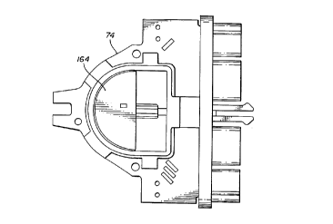
FIG. 1 illustrates a connector assembly 10 which is designed to
mate with the rear portion 12 of an IC (integrated circuit) card 14. The
connector assembly has a rear 16 that connects to a cable 20, and has a front
with plug parts 22 - 28 that are received in receptacle parts 30 of the IC
card.
The connector assembly has a latch mechanism 32 which includes a pair of
arms 34, 36 that can be received in a central aperture 40 at the rear of the
IC
card, to prevent the connector assembly from accidentally pulling out of the
card. The latching mechanism includes a locking pin 42 which can slide to a
position between front portions of the arms to prevent them from bending
together to release from the IC card.
As shown in FIG. 2, the connector assembly 10 includes a
connector subassembly 50 that includes all parts of the assembly except for a
molded overlayer 52. The subassembly includes a frame 54 with a front
portion 56 that includes a flange 60 which is wide in a lateral directions A
but
which is narrow in vertical directions U, D and which is narrow in
longitudinal
directions B. The longitudinal directions B include forward and rearward
directions F, R. The frame forward portion includes the plug parts 22 - 28
that
Y ..
WO 95117030 ~ ' 21 l 8 8 31 PC'TlUS94112705
-4-
project fonvardly of the flange. The forward portion has a row of passages or
contact-holding openings 61 that each holds a contact 62. Each contact has
a rearward end forming a tail 64, which must be connected to the bared front
end 66 of an insulated cable wire 70. The connections are made by soldering
the tail 64 and the wire front end 66 to any corresponding conductive trace 72
on a circuit board 74. The circuit board has a front end 76 that is connected
to the frame front portion, and has a rear end 78 that is coupled to the
stripped
front end or portion 80 of the cable 20.
The circuit board'74 is thin, having a thickness such as 0.55mm
in a connector having an overall thickness or height of about 5mm. To
securely hold the circuit board to the frame, applicant constructs the frame
with
a rearward extension 90. The rearward extension has a smaller lateral width X
(FIG. 4) than that Y of the flange. As shown in FIG. 3, the rearward extension
90 is initially molded separately from the front portion 56, and these
portions
are joined at surfaces 82, 84 and kept aligned by the rear ends of the arms
34,
36 which project through an opening 86. me rearward extension has a groove
92 lying in a horizontal plane (in the directions A and B), the groove having
laterally opposite groove sides 94, 96 at laterally opposite sides 97, 98 of
the
rearward extension. The rearward extension has a central part 99 that lies
between the groove sides. The board 74 has a slot 100 extending rearwardly
from the front end 76 of the board. The slot forms slot walls 102, 104 that
are
closely received in the groove sides 94, 96 when the board is slid in a
forward
direction F into the rearward extension 90 of the frame. This arrangement
results in the frame 54 of the connector assembly securely holding the circuit
board.
The circuit board has a rear end 78 with a slot 106 that receives
the stripped front end 80 of the cable 20. The insulated wires 70 of the cable
-WO 95/17030 ~ 21 ~ ~ $ 3 ~ PCT/US94/12705
-5-
preferably extend along the upper and lower surfaces 110, 112 of the board,
with applicant preferring to route most of the wires along the upper surface
of
the board. It may be noted that it is common for the cable to have many fewer
insulated wires than Lhe number of traces 72, so that wires are connected to
only some of the traces. The circuit board has a front portion 115 with first
and
second front side portions .114, 1 i 6 with traces 72 positioned to engage -
contact tails 64 at plug parts such as 22, 26 that lie on opposite sides of a
central passage 152.
The frame rearward extension 90 has tabs 120 - 127 projecting in
largely horizontal planes to lie over or under the board surfaces 110, 112.
The
tabs such as 120 are useful to hold down the cable wires 70. As shown in FIG.
7, each tab such as 120 is spaced from a corresponding board surface 110 by
a distance E which is about the same as the diameter F of a cable wire 70.
When the connector assembly is being fabricated, and the cable wires must be
routed to corresponding traces 76, the persons assembling the connector
slides the wires under the tabs such as i20 to hold the wires in position,
with
their bared forward ends 66 lying against corresponding traces 76. This helps
to locale the wires and their bared ends for soldering, as indicated at i30,
of
the wire ends to the traces. After all of the wires are routed and their ends
soldered to corresponding traces, with the contact tails 64 also soldered to
corresponding traces, the connector subassembly is placed in a mold. The
overlayer 52 (FIG. 2) is molded around all of the wires and most of the
subassembly rearward of the flange 60 to hold the parts in place.
As shown in FIG. 8, the latch mechanism 32 includes the arms 34,
36 which are designed to be received in the central aperture 40 of the IC card
14. The arms are deflected together as they are received in the aperture,
until
lateral projections 140 at the front ends of the arms, which extend away from
WO 95/17030 ~ F ' 217 8 8 31 pCT/US94112705
-6-
each other, lie against largely fonvardly-facing shoulder 142 formed at the
rear
of the walls of the card central aperture 40. The arms resist rearward
movement of the connector assembly 10, but, by themselves, do not lock the
connector assembly to the IC card.
The latch assembly 32 includes a locking pin 150 that is
longitudinally slidable within a central passage 152 formed in the frame 54 of
the connector assembly. When the locking pin i50 slides forwardly to the
position shown at 150A, it prevents the arms from moving together, and
thereby locks the connector assembly to the IC card. It may be noted that
basic latching mechanisms that include a pair of deflectable arms and a
locking
pin that can slide to a position between arms to prevent them from deflecting
together, is known in the prior art, as described in U.S. patent 4,362,348.
However, the latch mechanism 32 must be manually operated, and it can be
difficult to provide a manually operated handle for moving a locking pin in
the
i5 thin connector assembly which includes an injection molded overlay.
As shown in FIG. 3, the latch mechanism 32 includes a handle
160 with identical upper and lower handle parts 162, 164. Each handle part
has a post 166 that projects through a slot i70 in the frame rearward
extension
90. The post projects through a corresponding slot 172, 174 at the rear of the
locking pin, with the end of the post snapping into a snap hole 180 of the
opposite handle part. When the handle parts 162, 164 are slid forwardly, they
slide the locking pin 150 forwardly to lock the connector assembly to the IC
card, and when the handle is moved in the rearward direction R, it moves the
locking pin rearwardly to allow the connector assembly to be released. The
rearward extension 90 has smooth upper and lower surfaces 182 against which
the handle parts slide, with each handle part having a pair of slider bearings
184 with rounded surfaces for low friction sliding along the rearward
extension '
'WO 95/17030 217 8 B 31 p~~S94112705
_7_
surfaces. The rearward extension has a barrier 190 at its top and bottom which
surrounds the sliding surface 182 and which forms a recess 192 in which the
handle parts move. The barrier 190 prevents the flow of molding material into
the recesses 192 during molding of the overlayer. Thus, as shown in FIG. i,
the overlayer 52 surrounds all portions of the connector assembly rearward of
the frame flange 60, except for the recesses 192 and the barriers 190.
In a connector that applicant has made, of the construction
shown, the connector had a lateral width Y of 42mm and thickness of 4.9mm.
Each recess 192 had a depth of l.Omm, and each flat handle had a depth of
0.95mm. So long as the upper surface of a handle does not project above the
corresponding top or bottom surface of the frame by more than 509'0 of the
recess depth or by not more than 1 mm, it can be said that substantially the
entire handle thickness lies in the recess. Thus, each handle is flat and of
about the same thickness as a recess, and substantially the entire handle
thickness lies in a recess.
The presence of upper and lower handle parts 162, 164 facilitates
operation of the latching mechanism. A person presses his thumb and
forefinger (or other finger opposed to the thumb) respectively against the top
and bottom handle parts, to squeeze them together while sliding them forward
or rearward.
As shown in FIG. 8, the walls of the IC card central aperture 40
include a dust barrier 200 which closes the forward end 201 of the aperture.
The dust barrier 200 lies forward of a circuit board 202 of the IC card, and
prevents objects from being projected forwardly through the aperture 40, and
onto the circuit board 202, where the objects could short circuit traces of
the
board. As shown in FIG. 1, the IC card includes upper and lower covers 204
' which close the top and bottom of the rear 201 of the passage. The reason
WO 95/17030 ~ 217 8 8 3 l PCTlUS94/12705
_g_
why the top and bottom of the passage 40 is open, is to facilitate molding of
the passage, especially a recess at the rear that forms the shoulders 142.
While terms such as "top", "bottom" etc. have been used to aid in
the description of the invention, the connector assembly can be used in any
orientation with respect to gravity.
Thus, the invention provides a connector assembly that is
especially useful for mating with an IC card, wherein the connector assembly
is of rugged construction and can hold a compact manually operated latch
mechanism. The connector assembly includes a frame with a forward portion
having contact-holding passages, a circuit board extending rearward of the
frame, and a cable with a stripped front end coupled to the rear of the
circuit
board. The frame includes a rearward extension extending rearward of the
frame front portion. The rearward extension has a horizontal groove, and the
circuit board has a slot to enable slot walls to be closely received in the
groove.
i5 The rearward extension has tabs that are spaced slightly from the surfaces
of
the circuit board, to hold cable wires in place- A locking mechanism for
moving a latching pin between latching arms that project forwardly at the
front
of the frame, includes handle parts lying at the top and bottom of the
connector
assembly. The connector assembly includes an overlayer which surrounds all
of the connector assembly rearward of a forward flange, except for barrier
walls
and recesses therewithin in which the handle parts move.
Although particular embodiments of the invention have been
described and illustrated herein, it is recognized that modifications and
variations may readily occur to those skilled in the art, and consequently, it
is
intended that the claims be interpreted to cover such modifications and
equivalents.