Note: Descriptions are shown in the official language in which they were submitted.
CA 02179783 1999-06-10
V7:DE0 MAGNIFICATION APPARATUS
Field of the Invention
The present invention relates to video magnification
apparatus for shrinking or magnifying video graphics during a
transfer of the video graphics data signals from a graphics
memory to a television screen.
Background of the Invention
Some commercially available computers, particularly personal
computers, provide circuitry which permits a merger of a
composite video signal (e. g., a National Television Standards
Committee signal) with computer generated video graphics display
signals, typically red, green, and blue (RGB). More
particularly, modern video graphics equipment has the ability to
produce backgrounds, characters, symbols, and other pictorial
representations and arrangements in operator-selected sizes,
shapes, and colors.
1
~1~9~8~ ,
GID907
U.S. Patent No. 4,737,772 (Nishi et al.), issued on April
12, 1988, discloses a video display controller comprising a video
display processor (VDP), a Central Processing Unit (CPU), a
memory, and a Video Random Access Memory (VRAM). The memory
stores both programs to be executed by the CPU and various kinds
of image data. The VRAM stores image data which the VDP can
change and then transfer to the outside for display on a screen
of a Cathode Ray Tube (CRT) display. In the VDP, a timing signal
generator generates timing signals for correctly scanning
elements of the picture to be displayed which are used by a
horizontal and a vertical counter and the CRT display to
synchronize data processing in an image data processing circuit
(IDPC) and correctly display such processed data on the screen of
the CRT display. A Video Digitizer samples an externally
supplied analog video signal and converts signal levels or
amplitudes of the analog video signal into digital data composed
of 2 or 4 bits each. The Video Digitizer digitized amplitude
output data represents a still image and is supplied to the IDPC. -
The IDPC selectively stores both the Video Digitizer output data
and color codes supplied from the CPU into the VRAM through an
interface circuit. Each color code from the CPU represents a
color of a respective one of the display elements (e. g. pixel)
constituting a still image on the screen. In operation, in
response to a display command from the CPU, the IDPC sequentially
reads dot data from the VRAM in synchronization with the scanning
position on the CRT display and outputs the dot data to a color
palette circuit. Concurrently, the IDPC calculates and reads
2
GID907
data necessary for displaying an animation image from the VRAM
and supplies color codes to the color palette circuit. Where an
animation and still image are located at a same display position
on the screen of the CRT display, the animation image is
preferably displayed. The color palette circuit converts each
color code into three color data for red, green, and blue, each
composed of three bits. A Digital to Analog Converter (DAC)
converts the color data from the color palette circuit into R, G,
and B signals which are provided to the CRT display.
U.S. Patent No. 5,355,175 (Okada et al.), issued on October
11, 1994, discloses video mixing apparatus that mixes a graphics
video image and a playback video image at a plurality of mixture
ratios in one image plane. Fade data indicative of the mixing
ratio of at least one line of the playback video signal and the
graphics video signal is sequentially generated in accordance
with a predetermined order. The fade data is held in holding
means and is outputted from the holding means synchronously with
a horizontal sync signal. The levels of the playback video
signal and the graphics video signal are individually adjusted in
accordance with the fade data outputted from the holding means,
and the adjusted signals are added together. The playback video
signal and the graphics video signal are mixed at the mixing
ratio set for every line on one image plane to generate a video
output signal from the apparatus.
U.S. Patent No. 4,420,770 (Rahman), issued on December 13,
1983, discloses a video background generation system for
generating rectangular video patterns having operator-selected
3
a x
GID907
video attributes. The system comprises a horizontal bit memory
and a vertical bit memory, each of the memories being a 16 entity
memory for storing information for 16 background entities. The
memory for each background entity defines opposite.corners of the
background area for an entity on the screen. As shown in FIG. 2
of the patent, a first entity defines a first rectangular area, -
and a second higher priority entity defines a second partially
overlapping rectangular area. An attribute look-up table stores
information for each entity related to the color video output
(red, green, blue) for that entity. During the scanning of the
lines of a picture being produced, the first entity is produced
in its defined area and the second entity is produced in its
defined area. However, the second entity has a higher priority
which results in the overlapping region of the two entities to be
presented with the stored attributes of the second entity.
U.S. Patent No. 4,754,270 (Murauchi), issued on June 28,
1988, discloses digitized displaying apparatus which is capable
of enlarging or reducing a display size on the screen of a raster
scanning type display such as a CRT display. The apparatus
comprises an addressable memory means, input data means, and -
variable address data generating means. The addressable memory
means stores display data to be read out in a predetermined
timing relationship with a raster scanning of the display to
produce a display image. The input data means supplies numerical
data that determines image size. The variable address data
generating means includes variable addressing increments for
generating address data that is correlated with disglay data
4
~1'~~'~~3
GID907
addresses that are stored in the memory means to output the
display data. More particularly, the variable address data
generating means comprises arithmetic calculating means for
digitally calculating addressing increments in response to the
numerical data supplied by the input data means and to timing
signals related to the scanning of the display. The variable
address data generating means. is responsive to the arithmetic
calculating means to increment addresses for addressing the
memory means according to the numerical data that determines the
image size. More particularly, when displaying an original size,
a horizontal address of the memory means is incremented by a "1"
at every 200 nanoseconds. In other words, dot size in the
horizontal direction of the display is 200 nanoseconds for
displaying the original size. The size in the horizontal
direction can be enlarged or reduced by changing the displaying
time of one dot in the horizontal direction by properly selecting
addend data provided to the memory means. By the appropriate
setting of addend data supplied to the variable address data
generating means, the size of characters and the associated
images on the display screen can be enlarged or reduced with
respect to a nominal size.
Presently, there is emerging a need for interactive video
graphics which will enable a whole new class of services to be
delivered to the home via a cable television network. These new
services will.enhance the viewing experience for many traditional
television programs while providing augmented services to others.
However, NTSC and Phase Alternating Line (PAL) television -
5
~1'~9'~83
GID907
receivers, unlike computer monitors, have a fairly low video
bandwidth and employ an interlaced, not a progressive scan,
disnlav. These limitations place severe constraints on the
generation of an artifact free high resolution synthetic video
signal. Traditionally, consumer products, such as video games, -
avoid these problems by generating low resolution non-interlaced --
video signals. This approach results in images that are of low
quality, have a "blocky" appearance, are limited in color choice,
and take on a cartoon-like look.- The generation of synthetic
video that approaches broadcast quality requires that the
generated synthesized signals emulate that of a video camera _
scanning a scene and the subsequent analog signal processing for
such video camera signals. Therefore, it is desirable to provide -
a relatively inexpensive arrangement that permits good synthetic
video graphics to be overlaid on top of live television -
prograzzrcning for viewing on a standard NTSC or PAL standard
interlaced television receivers'with the ability to shrink or -.
magnify video graphics data during transfer from a Graphics
Memory to the screen of a television receiver.
$ ~~ of the Invention _ -
The present invention is directed to video magnification
apparatus for shrinking or magnifying video graphics during a
transfer of the video graphics data signals from a graphics
memory to a television screen. - _
Viewed from one aspect, the-present invention is directed to
apparatus for modifying the magnification of a graphic prior to
displaying the graphic on a.television receiver, the apparatus -
6
~~~~~~J
GID907
comprising first and second magnification modifying means. The
first magnification modifying means modifies the magnification of
a graphic by a first independent predetermined magnification
factor in a vertical direction by-generating graphic line address
output signals. The graphic-line address output signals are used
to selectively prevent a transmission of predetermined horizontal
lines of the graphic upon the reception of a vertical
magnification factor that is less than unity. Still-further, the
graphic line address output signals are used for causing a
selective repeating of the transmission of predetermined -
horizontal lines of the graphic upon the reception of a vertical
magnification factor that is greater than unity. The second
magnification modifying means is responsive to the transmissions
of horizontal lines of the graphic indicated for transmission by -
the graphic line address output signals of the first
magnification modifying means for modifying the magnification of
the graphic in a horizontal direction by a second independent
predetermined horizontal magnification factor. Still further,
the second magnification modifying means selects N predetermined
pixels of each received X pixel group that are multiplexed into
an transmitting X pixel group for transmission in each output
signal of the apparatus for a horizontal magnification factor -.
equal to or less than unity for transmission in each output
signal of the apparatus, where NsX. Additionally, the second
magnification modifying means causes a repeating of pixels of -
each received X pixel group by a predetermined integer amount
7
GID9b7
corresponding to a received horizontal integer magnification
factor that is greaterthan unity.
Viewed from another aspect, the present invention is
directed to apparatus for modifying the magnification of a
graphic prior to displaying the graphic on a television receiver
comprising vertical magnification modifying means. The vertical
magnification modifying means comprises magnification inverting
means and multiplying means. The magnification inverting means
inverts the value of a received vertical magnification factor and
generate therefrom an output signal representative of the
inverted magnification factor. The multiplying means is
responsive to the output signal from the magnification inverting
means and an input signal representing a number of a horizontal
line of the graphic currently being accessed for multiplying the
inverted magnification factor with the number of the horizontal
line to generate an output signal representing a line number of
the graphic to beaccessed.
Viewed from still another aspect, the present invention is
directed to apparatus for modifying the magnification of a
graphic prior to displaying an image of the graphic on a
television receiver comprising a horizontal magnification
modifying means comprising a pixel select Read-Only-Memory (ROM),
a multiplexer drive ROM, and pixel multiplexing means. The
pixel select ROM is responsive toe received horizontal
fractional magnification value for generating a horizontal
fractional magnification output signal indicating which pixels of
an incoming group of a plurality of X pixels are to be used in
8
X
~1'~9~~3
GID907
generating an output signal of the apparatus. The multiplexes
drive ROM is responsive to the horizontal fractional
magnification output signal and a received horizontal integer
magnification value for generating separate coded output signals
during sequential multiplexing cycles. The multiplexes drive ROM
coded output signals indicate which received pixels of an
incoming group of a plurality of Y pixels are to be multiplexed
into which output pixels of an outgoing group of a plurality of Y
pixels. The pixel multiplexing means is responsive to the coded
output signals from the multiplexes drive ROM and a reception-of -
the incoming group of the plurality of Y pixels for multiplexing
predetermined ones of the Y pixels of the incoming group into
predetermined ones of the plurality of Y pixels of the outgoing
group during each predetermined cycle to form an apparatus output
signal.
The invention will be better understood from the following
more detailed description taken with the accompanying drawings.
Brief Description of the Drawings
FIG. 1 is a block diagram of a subscriber cable box unit in
accordance with the present invention;
FIG. 2 is a block diagram of a first portion of a Video
Processing Circuitry found in the subscriber cable box unit of
FIG. 1 in accordance with the present invention;
FIG. 3 is a block diagram of a second portion of a Video
Processing Circuitry found in the subscriber cable box unit of
FIG. 1 in accordance with the present invention;
9
~1~~~83
GID907
FIG. 4 is a block diagram of an exemplary Pixel Assembly
Buffer forming part of a first portion of the Video Processing -
Circuitry shown in FIG. 2;
FIG. 5 is a block diagram of an exemplary Multiplexer/Fader
forming part of a second portion of the Video Processing
Circuitry shown in FIG. 3;
FIG. 6 is a block diagram.of an exemplary arrangement of a
Convolver forming part of the secand portion of the Video
Processing Circuitry shown in FIG. 3;
FIG. 7 is a block diagram of a Pixel Buffer Data Pipe and
Magnification Circuit forming part of the first portion of the
Video Processing Circuitry shown in FIG. 2 in accordance with the - -
present invention;
FIG. 8 shows a transfer of pixels between a 32-bit input
buffer and a 32-bit output buffer during a first Word/Time 0
cycle and a second Word/Time 1 cycle within a Pixel Multiplexer -
shown in FIG. 7 for a magnification of one in accordance.with the
present invention;
FIG. 9 shows a transfer of pixels between a 32-bit input
buffer and a 32-bit output buffer during a first Word/Time 0
cycle and a second Word/Time 1 cycle within a Pixel Multiplexer
shown in FIG. 7 for a magnification of one half in accordance
with the present invention;
FIG. 10 shows a;transfer of pixels between a 32-bit input
buffer and a 32-bit output buffer during a first Word/Time 0
cycle and a second Word/Time 1 cycle within a Pixel Multiplexer
~ N
~1"~~'~~3
GID907
shown in FIG. 7 for a magnification of two and one half in
accordance with the present invention;
FIG. 11 shows a first page of a multi-page spreadsheet
illustrating the operation of a Multiplexes Drive ROM shown in
FIG. 7 in accordance with the present invention;
FIG. 12 shows a middle page of a multi-page spreadsheet
illustrating the operation of a Multiplexes Drive ROM shown in
FIG. 7 in accordance with the present invention;
FIG. 13 shows a block diagram of a vertical logic circuit
for processing magnification factors in a vertical direction in _
accordance with the present invention;
FIG. 14 shows a circuit.diagram for a first portion of a
Pixel Buffer Data Pipe and Magnification Circuit shown in FIG. 7
in accordance with the present invention;
FIG. 15 shows a circuit diagram for a second portion of a
Pixel Buffer Data Pipe and Magnification Circuit shown in FIG. 7
in accordance with the present invention; and
FIG. 16 shows a block diagram of a Quad octal multiplexes
used within a Pixel Multiplexes included in a Pixel Buffer Data
Pipe and Magnification Circuit shown in FIG. 7 in accordance with
the present invention.
11
o k
GID907
Detailed Description
It is to be understood that corresponding elements
performing the same function in each of the figures have been
given the same designation number.
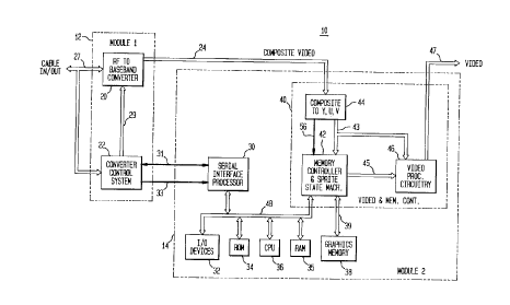
Referring now to FIG. 1, there is shown a block diagram of a
subscriber cable box unit 10 that can be found on a subscriber's
premises that provides interactive video processing in accordance
With the present invention. The subscriber cable box unit 10
comprises a first module (MODULE 1) i2 (shown within a first
~,0 dashed line rectangle) and a second module (MODULE Z) 14 (shown
within a second dashed line rectangle). The first module-12 is a
conventional arrangement that comprises a Radio Frequency (RF) to
Baseband Converter 20 and a Converter Control System 22, each of
which are known in the art. The RF to Baseband Converter 20
~5 receives multiplexed RF television channel signals in the NTSC or
PAL standard format propagating on a cable 27 from a remote cable
company central office (not shown), and selectively converts such
multiplexed RF television channel signals from their multiplexed.
channel frequencies to baseband frequencies. The RF to Baseband
~0 Converter 20 transmits a resultant baseband composite video
output signal from the conversion process over a bus 24 to the __
second module 14. The Converter Control System 22 is user -
(subscriber) is typically controlled by either an Infra Red
remote control device or a keypad on the cable box as is well
~5 known in the art. The Converter Control System 22 functions to
receive and/or transmit authorization and access control signals
via the cable 27 to or from a remote cable company central
12
~1~9~83
GID907
office, activate baseband video scrambling or descrambling, and
produce On Screen Display (OSD) messaging. The Converter Control
System 22 outputs control signals via a bus 29 to the RF to _
Baseband Converter 20 for selecting desired channel programming,
and various control and decrypted data signals (e.g., control and
upstream data output signals, Infra Red receive and transmit
signals, and decrypted T1 Quadrature Phase Shift Keying data
signals) via leads 31 and 33 to the second module 14. -
The second module 14 comprises a Serial Interface Processor
(SIP) 30, Input/output (I/O) devices 32, a Read Only Memory (ROM)
34, a Random Access Memory (RAM) 35, a Central Processing Unit
(CPU) 36, a Graphics Memory 38, and a Video and Memory Control
(VIDEO & MEM. CONT.) integrated circuit 40 (shown within a dashed
line rectangle). The SIP 30, I/O devices 32, ROM 34, RAM 35, CPU
36, and a Memory Controller and Sprite State Machine (MACH.) 42
of the Video and Memory Control integrated circuit 40 are
interconnected by a data bus 48. The CPU 36 can comprise any
suitable processing unit and, in accordance with the present
invention, is a 386 type CPU which is relatively inexpensive.
The ROM 34 can comprise any suitable memory ae, for example, an
EPROM for initialization purposes and for programming of the CPU
36. The RAM 35 can comprise any suitable memory as; for example,
two 256 Kilobyte-by-16 bit DRAMS connected in series to provide a
512K-by-16 bit RAM configuration for use as a scratchpad memory
for the CPU 36. The Graphics Memory 38 can comprise any suitable , ,
memory as, for example, a 32 bit wide RAM area or preferably two
256K-by-16 bit DRAMs arranged in parallel for use with a 32-bit
13
~1'~9'~83
GID907
wide bus 39. The Graphics Memory 38 is used to store sprite data
relating to graphics and video pictures. The use of a 32-bit
wide bus 39 permits the use of fast-page mode memory addressing
for both a Memory Controller and Sprite State Machine 42 and a
block memory mover (not shown) forming part of the Video and
Memory Controller 40. By significant use of block mode memory
addressing, an average data transfer rate of approximately 52 --
nanoseconds can be achieved, which corresponds to processing
approximately 77 million bytes of data per second.
~0 The SIP 30 functions to handle data communications between
the first module 12 and the second module 14. More particularly,
the SIP 30 handles all data transfer signals between the second
module 14 and the converter control system 22 of the first module
12. These data transfer signals can have formats such as, for
~5 example, a T1-like data stream at 1.5 Mbits/second which involves
the bulk of the communication transfers, and raw data from an
infrared receiver (not shown) in the converter control system 22.
The SIP 30 can also include a full duplex synchronous serial port
(not shown) for future expansion. Such data transfer signal
?0 formats are used to communicate between the converter control
system 22 on the first module 12 and the CPU 36 in the second
module 14 to activate desired actions in the second module 14.
The Video and Memory Control integrated circuit 40 comprises
the Memory Controller and Sprite State Machine 42, Composite to
?5 YW circuitry 44, and Video Processing (PROC.) circuitry 46. The
Memory Controller and Sprite State Machine 42 is coupled to the
Graphics Memory 38 by a data bus 39, and to the Video Processing
14
~
~1~~~83
GID907
circuitry 46 by a data bus 45. The Composite to YUV circuitry 44
receives the baseband composite video signal from the bus 24 and
outputs resultant YUV video signals to the Memory Controller and
Sprite State Machine 42 on a bus 43. The Video Processing
circuitry 46 receives video signals from the Memory Controller
and Sprite State Machine 44 over the data bus 45, and outputs
NTSC or PAL standard video signals on a bus 47 to a remote
television receiver (not shown) or to further processing
circuitry (not shown). It is to be understood that the present
invention lies within the area of the Video and Memory Control
integrated circuit 40 and the Graphics Memory 38. The elements
of the first module 12 and the second module 14 were introduced _
and discussed hereinbefore for a better understanding of how the
present invention fits into the interactive subscriber cable box
unit 10.
Referring now to FIGS. 2 and 3, there are shown block
diagrams of first and second portions, respectively, of a Video
Processing Circuitry 46 (shown within a first dashed line
rectangle) found in the second module 14 of the subscriber cable
box unit 10 of FIG. 1 in accordance with the present invention.
As is shown in FIG. 2, a Graphics Memory 38, forming an element
of the second module 14 of FIG. 1, is coupled for bidirectional
communication via a data bus 39 to a Memory Controller and Sprite
State Machine 42 which is part of a Video and Memory Controller
40 (shown within a second dashed line rectangle) found in the
second module 14 of FIG. 1.
~1~~'~83
GID907
The Memory Controller and Sprite State Machine 42 is coupled
to a Central Processing Unit (CPU) 36 (shown in FIG. 1) via a bus
48 for writing sprite information into the Graphics Memory 38 via
the bus 39, and receives a Field <1:0> signal from the Composite _
To Y,U,V circuitry 44 of FIG. 1 via conductor 56. This portion _
of the Video Processing Circuitry 46 further comprises a Data
Pipe 50 (shown within a dashed-line rectangle), and a Pixel
Assembly Buffer 52. _
The Graphics Memory 38 comprises multiple Tables comprising
a Sprite List table 90, a Sprite Data table 92, a Line Control _.
table 94, and a Span List table 96. These Tables are discussed
in great detail in copending Patent application Serial No.
08/523,394 (GID908-Butler et al.), filed on the same date as the
present application for the present assignee. More particularly,
the Sprite List table 90 comprises a separate memory section for
each of one or a plurality of-N sprites (only entries for sprites
#1, #2, and #N are listed). As is shown for the Sprite #1 entry,
the memory section therefor comprises a Sprite Data Pointer
portion, a Sprite Controls portion, a Line Table Pointer portion,
an Optional Controls portion, and a Field Enable Control portion.
The Sprite Data Pointer portion is used to access the Sprite Data
Table 92 at a predetermined location for pixel data for
horizontal lines associated with the Sprite Entry. The Sprite
Controls portion comprises data relating to, for example, the
size of the sprite, its X and Y location or position on the
screen of the television receiver, and special effects
information about magnification, warping, etc. that is to be
16
~~~9~83
GID907
performed on the sprite. More particularly, if the Sprite
Controls portion indicates that a sprite has a magnification of
2, then every line of the sprite is magnified by 2. Similarly,
if the Sprite Controls portion indicates that a sprite has an -
offset of 2, then all lines of the.sprite are offset by 2. In
other words, the Sprite Controls portion affects each horizontal
line of pixel data of the sprite the same way.
The Line Table Pointer portion of each Sprite Entry is used
to access a predetermined portion of the Line Control Table 94
for control words associated with that Sprite Entry in order to
produce more advanced special effects from that produced by the
Sprite Controls portion discussed above. Finally, the Field
Enable Control portion is used to produce desired "smoked glass~~
(transparent overlay) effects on the screen of the television -
receiver for the Sprite Entry being accessed in the Sprite Liat
table 90. Similar portions are shown for each of the other
sprite #2 to #N entries. Still further, the sprites in the
Sprite List table 90 are preferably listed in order of increasing
priority where, for example, the sprite #1 entry has a lowest
priority and the sprite #N entry has a highest priority. As a
result of such priority arrangement, pixels of a sprite with a
higher priority overwrite, replace, or take precedence over
pixels of a sprite with a lower priority where two sprites or a
sprite and live video are located in an overlapping location on a
screen of a television receiver.
The Sprite Data table 92 comprises data words including pure
data for each of the pixels of each horizontal line for each
17
21~9~83
GID907
Sprite Entry of the Sprite Liat table 90. In other words, when a
Sprite Entry is accessed in the Sprite List table 90, the Sprite
Data Pointer portion directs the access into the Sprite Data
table 92 where the Sprite Data words (e.g., Sprite A Data word to
Sprite C Data word) for that Sprite Entry are stored in the _
Sprite Data table 92 of the Graphics Memory 38. It is to be
understood that these Sprite Data Words do not include the
numerical number of lines in the sprite since the size of the
sprite, the location on the screen of the television receiver,
etc., for that sprite is located in.the Sprite Controls portion
of the Sprite List Entry. The Sprite List table 90 and the
Sprite Data table 92 work together by the Memory Controller and
Sprite State Machine 42 first accessing The Sprite List table 90
and then, under-control of, the Sprite Data Pointer portion,
accessing the Sprite Data table 92 to retrieve the data that
tells the Video Processing Circuitry 46 to draw the sprite in the
mannerdescribed by the Sprite Data words.
The Line Control Table 94 of the Graphics Memory 38 is an
optionally used table that contains subtables of separate
predetermined lengths (only one subtable is shown including N
control words), where each subtable comprises a separate line
control word for each line of a sprite. The line control words
in the Line Control Table 94 provide independent controls for the
horizontal lines of that sprite. More particularly, as stated
hereinabove, the Sprite Controls portion of each Sprite Entry in
the Sprite List table 90 affect every line of a sprite in the
same manner. In contrast, the Line Control Words in a aubtable
18
~1'~9'78J
GID907
in the Line Control Table 94 for a Sprite Entry, as pointed to by
the Line Table Pointer portion of the Sprite List table 90, are
used to provide independent controls for each of the horizontal
lines of that sprite. For example, it is assumed that the Sprite
Controls portion for the Sprite #1 Entry indicates that the
Sprite #1 image includes ten lines at a location X and Y on the
screen of. the television receiver without any special effects
such as constant offsets. The pixel data for each of the ten
lines of the Sprite #1 image is provided in the Sprite Data table
92 beginning at the address therein indicated by the Sprite Data
Pointer portion of the Sprite #1 Entry. Special effects that
might be used for any one or more of the ten lines of Sprite #1
are found in certain ones of the line control words in the Line
Control Table 94 beginning at the address indicated by the Line
Table Pointer portion of the Sprite #1 Entry. In other words,
the edges of the image of Sprite #1 might be aligned in a
straight line on the screen of the television receiver. However,
with the line control words of the Line Control Table 94, each
line of Sprite #1 Entry can have, for example, different offsets
for warping the image in a predetermined manner. For example, a
sprite image can be warped using the associated line control
words Line Control table 94 to appear on the outside surface of a
three-dimensionally drawn cylinder.
The Span List table 95 is an optional table which is used to
save time in processing many Sprite Entries in the Sprite List
table 90. In prior art systems, each of the Sprite Entries in a
Sprite List table 90 are sequentially entered to determine if
19
~
~1'~~'~~~
GID907
that sprite exists in a pixel~being assembled for a horizontal
line using the size and the X and Y location on a display screen
designated for that sprite. As a result, the prior art systems,
for example, for playing games were limited to a few number of
sprites (e. g., N=8 or 16 sprites) in order to assemble the pixels
for each line within the time period necessary for displaying _
such horizontal line on the display screen.
In the present subscriber cable box unit 10, without the _ _
optional Span List table 96 being present, the Memory Controller
and Sprite State Machine 42 normally accesses each of the
plurality of N Sprite Entries listed in the Sprite List table 90
of the Graphics Memory 38 in sequence to determine which of the N
Sprite Entries exist in each pixel of the horizontal line being
assembled. In accessing each of the N Sprite Entries of the
Sprite List table 90, the Memory Controller and Sprite State -.
Machine 42 obtains the data from the Sprite Data table 92 and the
optional Line Control Table 94 effects needed for each sprite to
produce the pixel data for each horizontal line being assembled
in the Pixel Assembly Buffer 52. However, if the Memory
Controller and Sprite State Machine 42 has to access and process,
for example, 96 different Sprite Entries, the time necessary to
process the 96 sprites would exceed a time period perrttitted for
assembling each horizontal line of pixel data in the Pixel
Assembly Buffer 52. The use of the Span List table 96 overcomes
this problem.
Where the optional Span List table 96 is used, at least one
register (not shown) in the Memory Controller and Sprite State
~~~~~~J
GID907
Machine 42 indicates that the Span List table 96 exists, and
provides all the data necessary for the Memory Controller and
Sprite State Machine 42 to properly use the Span Liat Table 96,
including a portion designated "# Sprite Entry Words" which
contains a number (integer value) of words (NW) per Sprite List
Entry which is a constant integer value for each of the Sprite
Entries when the Span List table 96 exists. More particularly,
each Sprite Entry in the Sprite List table 90-can include words
for (1) a Sprite Data Pointer, (2) Sprite Controls, (3) an
optional Line Table Pointer word, (4) an optional word for
Optional Sprite Controls, and (5) an optional Field Enable
Control Word. Therefore, each Sprite Entry of the Sprite List
table 90 can contain from 2-5 words. When a Span List table 96 -
is used, each of the Sprite Entries of the Sprite List 90
includes a same number of words (e.g., 5 words) regardless of
what optional words are normally required for each Sprite Entry.
The purpose of the register which indicates the Number of Sprite
Entry Words in each Sprite Entry is to simplify an accessing of
only certain ones of the Sprite Entries of the Sprite List table
90 when building the pixels of a horizontal line.
The Span List table 96 comprises one span list control word
or a group of span list control words that describe which of the
N sprites found in the Sprite List table 90 exist in each line of
a separate one of an arbitrarily defined plurality of horizontal
sections of a television screen. It is to be understood that the
Span List table 96 is primarily used where there are many sprites
(e.g., N=96 sprites) in order to reduce processing time in
2I
GID907
assembling the pixel data for each of the horizontal lines in the
Pixel Assembly Buffer 52. The number of words in the Span Liat
table 96 is dependent on the Equation:
No. of Span List words = (NS/32)*(NH/NL), Eq. 1
where NS is the number of total sprites on the display screen, NH
is the number of lines in the display screen, NL is the number of -
lines on the screen of a television receiver per span list word
or group of words, and 32 represents the exemplary number of bits
available in each word of the Span List table 96. The values for
NH and NL are programmable numbers, and NL can have a value of,
for example, 2, 4, 8, 16, 32, 64, or 128. More particularly,
although there electrically are 525 horizontal lines of video in
two fields of a standard NTSC television display, only about 440-
500 lines are normally seen depending on the television receiver
used. The display area of the screen where the 96 sprites are to
displayed can vary from 0-500 lines for any predetermined number
of sections, where each section has an equal number (NL) of -
lines.
In operation, the Memory Controller and Sprite State Machine
42 determines from the one or more registers therein that a Span
List table 96 exists, also obtains the data (NS, NH, and NL
values, the start line for the display area, and the number of
sprites) that are stored therein and needed for use with the Span
List table 96, and determines the number of Span List words
needed for each section of the display area in accordance with -
Equation 1 above. In assembling the pixel data for the 525 lines
of the video display, when the Memory Controller and Sprite State
22
~1~~~83
GID907
Machine 42 reaches the start line for the Span List display area
the Memory Controller and Sprite State Machine 42 first accesses
the Span List words (e.g., first three words) associated with a
top section of the span list display area. From these first
three words of Span List table 96, the Memory Controller and
Sprite State Machine 42 determines that, for example, only Sprite
Entries 1, 2, 4, and 6 are active in this section.
It is to be understood that the Memory Controller and Sprite
State Machine 42 uses a same one or more Span List words for each
of the lines of a section since the same sprites are active in
each of the lines of that section. The Memory Controller and
Sprite State Machine 42 operates in the same manner for each of
the other sections of the display area covered by the Span List
words.
The Field Enable Control portion of each Sprite Entry in the
Sprite List table 90 relates to controls for forming a "Smoked
Glass" (transparent overlay) effect with two sprites or one
sprite over live video. More particularly, a~"smoked glass"
effect is defined as an overlapping area of two sprites, or one
sprite over live video, where a first sprite is displayed on the
screen of a television receiver on lines (e.g., even lines) of a
first field of a picture, and a second sprite or live video is
displayed on the screen of a television receiver on lines (e. g.,
odd lines) of a second field of a picture. Such effect allows an
image of the first sprite to be seen while also seeing an image
behind it of the second sprite which can be, for example, a
captured snapshot of a frame of a live video that is stored as a
23
~1?9783 GID907
Sprite Entry in the Graphics Memory 38, or actual live video.
The two dimensional Convolver 68 then processes the assembled
image to produce a "Smoked Glass" effect between the two sprites.
Prior art systems primarily use software to computationally
combine two images.
In accordance with the present invention, the Field Enable
Control portion of the Sprite Entry indicates that this Sprite is -
only to be displayed in the even-numbered or odd-numbered lines
of the area of the display screen indicated for that sprite.
When assembling the pixel data in each horizontal line of a
display for the Sprite Entries of the Sprite List table 90, the
Field Enable Control indicates whether such sprite exists on a
horizontal line or not with its designated area on a display
screen. This is a simple and inexpensive method of permitting a
graphic or sprite to be inserted or turned on in just one of the
two fields.
In order for the Memory Controller and Sprite State Machine
42 to produce the "Smoked Glass" effect, it needs to know which
field is currently being displayed on the screen of the
television receiver. This information indicating the current
video field is provided tothe Memory Controller and Sprite State _-
Machine 42 by a 2-bit field signal (FIELD <1:0>, which indicates
bits 1 and 0) transmitted by a remote video sync circuit (not
shown) generally located at the Composite To Y,U,V circuitry 44
(shown in FIG. 1) of the subscriber cable box unit 10 and
obtained from a received live video signal stream. This 2-bit
Field signal is basically a continuously running clock signal.
24
GID907
The Memory Controller and Sprite State Machine 42 also reads
a 4-bit Field Enable control from the associated Sprite List
Entry which indicates which field to enable of two frames stored
for a sprite. It is to be understood that the entire information
for the colar of a color pictureis transmitted within four
fields of two frames in order to explain why four bits are needed
for the Field Enable Signal, where each frame has two fields.
Still further, the use of the two frames is not a matter of
displaying the color picture, but instead it becomes a matter of
the artifacts (e.g., flickering, etc.) produced on the screen of
an interlaced television receiver. More particularly, in an NTSC
color video signal, there are (a) 227.5 color bursts sent in each
horizontal line of the picture, (b) 262.5 lines for each of two
fields of a frame, and (c) 525 lines in a frame comprising the
two fields. Because there are 227.5 color burst per line, if the
color bursts on line 0 of field 0 go in a positive direction at a
certain point,then on the next line (line 2) of field 0 the
color bursts go in a negative direction at a certain point
because each line contains a sequence of whole color burst plus a
half of a color burst rather.than a sequence of just whole color
bursts. Still further, because there are an odd number of lines
(525) in a frame, the color-bursts in the first line (line 0) of
field 0 of the next (second) frame will go in a negative
direction and will be opposite in direction from color bursts in
line 0 of field 0 of the immediately previous frame. Thus, to
get a positive going color burst in line 0 of field 0 of a frame,
the repeat pattern only occurs every second frame. It is to be
x
~179~~3
GID907
understood that the whole content for a color picture is present
after the first frame, but that the repeat patterns of the
artifacts (e. g., flickering, etc.) are a by-products of a four
frame cycle. This is a result of a compromise originally made in
forming the NTSC standard for transmitting color television
signals that are compatible With black-and-white television
signals.
When a snapshot of a live television picture is placed into
the Graphics Memory 38 as a Sprite Entry in the Sprite List table-
~0 90, only one frame comprising two fields needs to be stored to
subsequently re-display the picture on the screen of a television
receiver. The 4-bit Field Enable control is used by the Memory
Controller and Sprite State Machine 42 to indicate when a sprite
is to be accessed in a certain frame or field depending on the
~S code of the four bits. For example, a "1" in bit three of the
Field Enable signal indicates that the associated sprite should
be enabled in frame 1, and a "1" in bit two of the Field Enable
signal indicates that the associated sprite should be enabled in
frame 0. Similarly, a "1" in bit one of the Field Enable signal
~0 indicates that the associated sprite should be enabled in field
1, and a "1" in bit zero of the Field Enable signal indicates
that the associated sprite should be enabled in field 0.
Therefore, bits 3 and 2 are used for double frame buffered
sprites while bits 1 and 0 are used to either produce a "smoked
~5 glass" effect where the sprite is only seen in one field, or for
double frame buffered sprites where a sprite is seen in both .
fields. The Memory Controller and Sprite State Machine 42
26
~~°~~'~83
GID907
compares the Field and Field Enable signals to determine which of
the four unique fields in the two frames is currently turned on
in order to display the sprite in its desired horizontal line
locations, and for remodulation to the NTSC picture to be
displayed on the television receiver screen by remote processing
circuits (not shown) to provide correctly directed color bursts.
More particularly, the information for the four field, as
determined from the Field and Field Enable signals, is used for
double line buffering in the Pixel Assembly Buffer 52 to
0 determine which sprite data is to be placed in each pixel
location of the Double Line Buffers 53, 54, and 55 (shown only in
FIG. 4). When the comparison of the Field and Field Enable
signals indicate a match of fields, the sprite data is read from
the Sprite Entry table 90, the Sprite Data Table 92, and the Line
5 Control table 94 in the Graphics Memory 38, and Double Line
Buffers 53-55 (shown only in FIG. 4) in the Pixel Assembly Buffer
52 are appropriately loaded during a certain field or frame. A
register (not shown) in the Memory Controller and Sprite State
Machine 42 is updated from the CPU 36 via bus 48 when necessary
'0 to indicate which field and/or frame is desired for loading the
data of a Sprite Entry in the Sprite List table 90 into the Pixel
Assembly Buffer 52.
The use of simple control words or groups of bits, and a
comparator-for comparing Field and Field Enable signals to
'S determine repeat patterns in horizontal lines of NTSC video
signals permits a "smoked glass~~ effect to be formed on an
interlaced display: This ie in contrast to performing the same
27
~1~~'~83
GID907
functions all in software that requires a powerful and typically
relatively expensive software processor with a great deal of -
programming as is found in some prior art systems. In such prior
art systems the processor (e. g., CPU 36 in FIG. 1) takes a part
in building the picture which requires a relatively expensive CPU
36, and if-the processor shuts down the building of the picture
stops. An advantage of the present subscriber cable box unit 10
is that if the CPU 36 shuts down, any animation of the picture _
being displayed stops because the CPU 36 is not providing
~0 information of what things to move around. However, the picture
is self-sustaining. More particularly, as long as the Graphite
Memory 38 is not corrupted, the video graphics portion of the
Video and Memory Controller 40 shown in FIGS. 2, 3, and 9 knows
how to build the picture from data in the Graphics Memory 38.
~,5 Returning now to FIG. 2, the first portion of the Video _
Processing Circuitry 46 comprises a Data Pipe 50 (shown within a
dashed line rectangle), and a Pixel Assembly Buffer 52. The Data
Pipe 50 comprises a Pixel Buffer Address Generator 97 and a Pixel
Buffer Data Pipe and Magnification Circuit (PIXEL BUFFER DATA
~0 PIPE AND MAG. CKT.) 98. The Pixel Buffer Address Generator 97
and the Pixel Buffer Data Pipe and Magnification Circuit 98 each
receive control data over a bus 45 that was obtained by the
Memory Controller and Sprite State Machine 42 from the Graphics
Memory 38, and the Pixel Buffer Data Pipe and Mag. circuit 98
25 also receives Sprite data over the Memory Data Bus 39, for a
particular sprite for transmission to the Pixel Assembly Buffer
52. The Pixel Buffer Address Generator 97 transmits address -
28
~1~9~83
GID907
output signals while the Pixel Buffer Data Pipe and Magnification
Circuit 98 transmits control and data output signals to the Pixel
Assembly Buffer-52 via respective buses 49 and 51. The Pixel
Buffer Address Generator 97 and the Pixel Buffer Data Pipe and -
Magnification Circuit 98 use pixel data obtained from a Sprite -
Control word in a Sprite Entry, a Sprite Data table 92, and any
other information from a Line Control table 94 in the Graphics
Memory 38 to place the data for each pixel of a horizontal line
of pixels in an appropriate address location within Double Line
Buffers 53, 54, and 55 (shown only in FIG. 4 and discussed
hereinafter) of the Pixel Assembly Buffer 52. Special effects
like magnification, warping, etc. to be performed on horizontal
lines of a Sprite Entry are obtained from the Sprite Control
words in the associated Sprite Entry and from any associated line
control words in the optional Line Control table 94 of the
Graphics Memory 38. The Pixel Buffer Address Generator 97 of the
Data Pipe 50 uses this information to appropriately alter the
pixel address in a line of. sprite data obtained from the Sprite
Data table 92 of the Graphics Memory 38 to achieve the designated
special effect. This altered address is sent to the Pixel
Assembly Buffer 52 via bus 49 for use in placing the associated
pixel data in the pixel location designated by the altered
address in: the Double Line Buffers 53, 54, or 55 of the Pixel
Assembly Buffer 52 to subsequently provide the designated special -
effect on the television screen. The Pixel Buffer Data Pipe and
Magnification Circuit 98, which is discussed in greater detail
hereinafter, concurrently receives the pixel data for the pixel
29
~~7~~~~
GID907
address, and transmits the pixel data to the Pixel Assembly
Buffer 52 for-storage at the address of the Double Line Buffer
53, 54, or 55 generated by the Pixel Buffer Address Generator 97.
The Pixel Assembly Buffer 52 outputs luminance pixel data for
three adjacent horizontal lines of any sprite to be displayed on
those lines on bua3es designated LINE 0, LINE 1, and LINE 2, and
outputs chrominance pixel data associated with the LINE 1
luminance output data on a LINE 1c.
Referring now to FIG. 4, there is shown a block diagram of a
i-0 Pixel Assembly Buffer 52 in accordance with the present
invention. The Pixel-assembly Buffer 52 comprises first,- second,
and third double line buffers 53, 54, and 55, respectively, and a
Y/G Line 0 buffer 58. The first double line buffer 53 is used
for storing Y/G (luminance) line 1a data and Y/G line ib data for
first and second lines of a first field of a sprite picture
received via a bus 49 from the Data Pipe 50. The line luminance
data comprises 10 bits (bits 9-0) of data and control for each
pixel of a line. The second double line buffer 54 is used for
storing C (chrominance) Line 1a and C Line 1b data of the first
and second lines of bhe first field of the sprite picture
received via the bus 49 from the Data Pipe 50. The line
chrominance data comprises 8 bits (bits 7-0) of data for each
pixel of a line. The third double line buffer 55 is used for
storing Y/G (luminance) line 2a data and Y/G line 2b data of
first and second lines of a second field of a sprite picture
received via the bus 49 from the Data Pipe 50. The line
luminance data comprises 10 bits (bits 9-0) of data and control
~ ~'~'~'~ 8 3
GID907
for each pixel of a line. Addresses for storing the received
pixel data in each of the first, second, and third double line
buffers 53, 54, and 55, respectively, are received over a bus 49
from the Data Pipe 50.
It is to be understood that the Lines la and 2a of the first
and third double line buffers 53=and 55 store first and second
horizontal lines of pixel data, respectively, where the first and
second horizontal lines are adjacent lines within separate fields
of the sprite .picture in an interlaced display format.
Similarly, Lines lb and 2b of the. first and third double line
buffers 53 and 55 store third and fourth horizontal lines of
pixel data, respectively, where the third and fourth horizontal
lines are adjacent lines within separate fields of the sprite
picture in an interlaced display format. In other words, the
first and third double line buffers 53 and 55 sequentially store -
luminance data and control for, for example, pixels of a pair of
odd and even lines, respectively, of respective first and second
fields, or vice versa, of the sprite picture during a scanning of
an interlaced display format. The second double line buffer 54
stores the chrominance data for the data of lines stored in the
double line buffer 53. A chrominance double line buffer (not
shown) similar to double line buffer 54 can be provided for
double line buffer 55, but it is not necessary for reasons of
economy and unimportance in a Convolver that will be explained -
hereinafter.
The output data from the first double line buffer 53_
comprises ten bite of luminance data and control for each pixel
31-
~i~s~s~
GID907
of the lines stored therein which-is outputted in parallel for
each pixel over a bus designated LINE 1 to circuitry in FIG. 3.
The output data from the second double line buffer 54 comprises
eight bits of chrominance data for each pixel of the lines stored
therein which is outputted in parallel for each pixel over a bus
designated LINE lc to circuitry in FIG. 3. The output data from
the third double line buffer 55 comprises ten bits of luminance
data and control for each pixel of the lines stored therein which
is outputted in parallel for each pixel over a bus designated
LINE 2 to circuitry in FIG. 3 and to the Y/G Line 0 Buffer 58.
The Y/G Line 0 Buffer 58 functions to delay the line data and
control outputted by the third double line buffer 55 by one
horizontal line period to provide a delayed line output
comprising ten bits of luminance data and control for each pixel
of the line stored therein which is outputted in parallel over a
bus designated LINE 0 to circuitry in FIG. 3. It ie to be __-
understood that at a sampling rate of 13.5 MHz for the NTSC
standard television display, there are 858 pixels per line of the
picture of which only about 704 pixels are actually displayed,
and that there are 525 horizontal lines of pixels in two fields
of a picture of which about 440-500 lines are normally seen
depending on the television receiver used.
An exemplary sequence of operation for the first and third
double line buffers 53 and 55, respectively, and the Y/G Line 0
Buffer 58 of the Pixel Assembly Buffer 52 is described in a
copending Patent Application entitled "Apparatus Using Memory
Control Tables Related To Video Graphics Processing For TV
32
~
~1~9~83
GID907
Receivers", Serial No. 08/523,394 (GID908) (Butler et al.), filed
on the same date as the present application.
More particularly, during initialization steps, pixel data
for a horizontal line 1 of a first field and pixel data for a -
horizontal line 2 of a second field are inputted to the Y/G line
la portion of the first double line buffer 53 and the Y/G line 2a ,
portion of the third double line buffer 55, respectively, during
a first horizontal line period. Concurrent therewith, the pixel
data for horizontal lines previously stored in the Y/G line lb
portion of the first double line buffer 53 and the Y/G line 2b
portion of the third double line buffer 55, respectively, (no
data presently stored therein) are read out on their respective -
output LINES 1 and 2. Concurrent therewith, the pixel data for
the horizontal line previously stored in the Y/G line 2b portion
of the third double line buffer 55 (no data previously stored
therein) is inputted to Y/G Line 0 Buffer 58 while the previously
stored pixel data for a horizontal line (no valid data) is
outputted on output LINE 0. Similarly, pixel data for a
horizontal line 3 of a first field and pixel data for a
horizontal line 4 of a second field are inputted to the Y/G line
lb portion of the first double line buffer 53 and the Y/G line 2b
portion of the-.third double line buffer 55, respectively, during
a second horizontal line period. Concurrent therewith, the pixel
data for horizontal lines 1 and 2 previously stored in the Y/G
line la portion of the first double line buffer 53 and the Y/G
line 2a portion of the third double line buffer 55, respectively,
are read out on their respective output LINES 1 and 2. Still
33
~
21~~y~$~
GID907
further, the pixel data for the horizontal line 2 previously
stored in the Y/G line 2a portion of the third double line buffer
55 is inputted to Y/G Line 0 Buffer 58 while the previously
stored pixel data for a horizontal line (no valid data) is
outputted on output LINE 0.
After initialization, pixel data for a horizontal line 5 of
a first field and pixel-data for a horizontal line 6 of a second
field are inputted to the Y/G line 1a portion of the first double
line buffer 53 and the Y/G line 2a portion of the third double
line buffer 55, respectively, during a third horizontal line
period. Concurrent therewith, the pixel data for the horizontal
lines 3 and 4 are read out of Y/G line 1b portion of the first
double line buffer 53 and the Y/G line 2b portion of the third
double line buffer 55, respectively, on their respective output
LINES 1 and 2. Still further, the pixel data for the horizontal
line 4 from the Y/G line 2b portion of the third double line
buffer.55 is inputted to Y/G Line 0 Buffer 58 while the
previously stored pixel data for the horizontal line 2 data is
outputted on output LINE 0. Therefore, the Buffers 58, 53, and
55 are outputting pixel data for the horizontal lines 2, 3, and
4, respectively, for a sprite on respective output LINES 0, 1,
and 2 during the third horizontal line period, where the pixel
data for the horizontal lines 2 and 4 are part of the second
field and the pixel data for the horizontal line 3 is part of the
first field of a sprite picture that were stored in the Graphics
Memory 38. The process continues in a similar manner during
34
~1~~7'~83
GID907
subsequent horizontal line periods for pixel data for subsequent
sequential horizontal lines.
Turning again back to FIG. 3, there is shown a block diagram
o~ a second portion of a Video Processing Circuitry 46 found in
the subscriber cable box unit 10 of FIG. 1 in accordance with the
present invention. The second portion of the Video Processing
Circuitry 46 comprises Color Palette circuitry 60, a YC to YW
Demultiplexer 62, a Multiplexer/Fader (MUX./FADER) 64, a 3:1
Multiplexer and Control (3:1 MUX. & CONT.) 66, and a Convolver
68. The 10-bit pixel data (bits 9:0) propagating on each of
LINES 0, 1, 2 from the output of the Pixel Assembly Buffer 52 of ..
FIG. 2 for corresponding pixels in three adjacent horizontal -
lines of a sprite picture are received at separate inputs of each
of the Color Palette circuitry 60, the YC to YW Demultiplexer 62
and the 3:1 Multiplexer and Control 66. More particularly, bits
7-0 of the parallel 10-bit/pixel output from the Pixel Assembly
Buffer 52 for each of output LINES 0, 1, and 2 are received at
the inputs of the Color Palette circuitry 60 and the YC to YW
Demultiplexer 62, while bits 9 and 8 of the parallel 10-bit/pixel
output from the Pixel Assembly Buffer 52 for each of output LINES
0, 1, and 2 are received at the inputs of the 3:1 Multiplexer and -
Control 66. Additionally, the YC to YW Demultiplexer 62
receives the chrominance data bits 7-0 outputted in parallel on
output LINE 1c from the Pixel Assembly Buffer 52 since the
chrominance data is only used when the sprite pixel data relates
to a True Color sprite signal. More particularly, where sprite
data is encoded as a color palette signal, the code itself
~1'~~"l~~
GID907
defines the color, and chrominance data is not required as is
needed-with a true color video signal.
The Color Palette circuitry 60 functions to detect when the
8 bits (bits 7:0) of parallel received pixel data on each of
output LINES 0, 1, and 2 representseparate codes for particular
colors of a color palette, and to convert those color palette __.
codes into an output signal on bus 61 representing a 24-bit YW
multiplexed color palette signal for three 8-bit pixel data
received for those three lines. Color Palette circuitry 60 is a
well known device, and any suitable circuit can be used therefor.
The YC to YUV Demultiplexer 62 detects when 8 bits (bits 7:0) of
parallel received data for pixels on each of the output LINES 0,
1, and 2 from the Pixel Assembly Buffer 52 represents true color -
data (e. g., a sprite obtained directly from a television
picture), and also uses the 8-bit chrominance data obtained via
output LINE lc from the Pixel Assembly Buffer 52 to generate a
24-bit True Color YUV output signal for pixels of the three lines
for transmission on bus 63.
The Multiplexer/Fader (MUX./FADER) 64 receives, at separate
inputs thereof, each of the 24-bit color palette YW data signals
propagating on a-bus 61 from the Color Palette circuitry 60, the-
24-bit true color YUV data signals propagating on bus 63 from the
YC to YW Demultiplexer 62, and 24-bit YW live video signals on
a bus 59. The Multiplexer/Fader 64 is responsive to control
signals on a lead 67 from the 3:l~Multiplexer and Control 66 to
output one of the three input signals (24-bit color palette YUV,
24-bit true color YW, or 24-bit live video YW) received at the
36
~1~9~83
GID907
Multiplexer/Fader 64 during each pixel period as digitized YUV
mixed output signals on a bus 65. More particularly, the 3:1
Multiplexer and Control 66 determines from the bits 9 and 8
received on the output LINES 0, 1, and 2 from the Pixel Assembly
Buffer 52 whether the pixel--data from the Pixel Assembly Buffer -
52 on the output LINES 0, 1, and 2 represents color palette data,
true color data, or data (non-valid data) for a pixel that is not
part of a sprite to be overlaid on a live video signal, and,
therefore, the live video signal should be used for that pixel
instead of the color palette or true color data received from the
Pixel Assembly Buffer 52. As a result of such control
information obtained from bits 9 and 8 of output LINES 0, 1, and
2 from the Pixel Assembly Buffer 52, the 3:i Multiplexer and -
Control 66 sends control signals over the lead 67 to the
Multiplexer/Fader 64 to select the correct input data for each
pixel of a picture to be displayed on a remote NTSC or PAL
television receiver (not shown). The Convolver 68 uses -
sequential sets of three pixel-data values received in the signal
from the Multiplexer/Fader 64 on bus 65 to provide an 8-bit
weighted output signal for pixel data for a central pixel in a 3-
by-3 matrix of corresponding pixels in three adjacent lines of a
television picture or to provide the signal received from the
Multiplexer/Fader 64 on bus 65 as a YUV output signal on bus 47
depending on control signals from the 3:1 Multiplexer and Control
66 over a lead 69.
Referring now to FIG. 5, there is shown a block diagram of
an exemplary Multiplexer/Fader circuit 64 (shown within a first
37
~1"~9'~8~
GID907
dashed line rectangle) which comprises a 2:1 Multiplexes (MUX.)
72, and a Fades 74 (shown within a second dashed line rectangle).
The Fades 74 comprises an A-B Adder 75, a Signed Multiplier
(SIGNED MULT.) 77, and an A+B Adder 78. The 2:1 Multiplexes
receives each of the Graphic data signals from the Color Palette
60 on bus 61 at a first input terminal (A), and the Graphic data
signals from the YC to YUV Demultiplexer 62 on bus 63 at a second
input terminal (B). A control signal on lead 67 from the 3:1
Multiplexes and Control 66 selects which of the two Graphic input
signals (from input terminal A or B) will be output from the 2:1
Multiplexes 72 at output terminal (O). Pixel Graphic output
signals (Y, U, or V) from an output terminal (O) of the 2:1
Multiplexes 72 (designated G) on a bus 70 are received at a first
input terntinal (A) of the A-B Adder 75. A live video YUV signal _
(Y, U, or V) (designated L) is received from a bus 59 at a second
input terminal (B) of the A-B Adder 75. The pixel data values of
the A terminal input data from the 2:1 Multiplexes 72 less the
data values of the live video YUV pixel data received the B input
terminal is provided as an output at an output terminal (O) of
the A-B adder 75. The Signed Multiplier 77 receives from, for
example, a register (not shown) a 9-bit selectively changeable -.
ratio control value (R) on a bus 71 at a first input terminal
(A), and the output from the A-B Adder 75 on a bus 76 at a second
input terminal (B). The resultant multiplied value of the ratio
control value (R) on the bus 71 and the Graphic signal output
data from the A-B Adder 75 on the bus 76 is output at an output
terminal (0) on a bus 79 to a first input terminal (A) of the A+B
38
21'~9'~83
GID907
Adder 78. The live video signal (Y, U, or v) on bus 59 is
received at a second input terminal (B) of A+B Adder 78, and the
sum of the two input signal.values are provided as a output
signal (designated Q) on the bus 65 to a Convolver 68 (shown in
FIG. 3). -
The Fader 74 functions to ~ade a graphic signal for a sprite
in or out so that the graphic does not appear or disappear
instantaneously over the live video signal. In other words, for
a graphic fade-in, the Fader 74 causes the graphic to appear with
increasing intensity on a television receiver while the live
video signal decreases in intensity in the area of the graphic
over a short period of time so that the graphic is totally -
visible. Similarly, for a graphic fade-out, the Fader 74 causes
the graphic to appear with decreasing intensity on a television
receiver while the live video signal increases in intensity in
the area of the graphic over-a short period of time until the
graphic disappears. The operation of the Fader 74 can be
explained in accordance with the following algorithms. For the
following, an exemplary 9-bit fade multiplier (R) provided on bus
71 is defined as follows. R is the fade control value and ranges
from 0 to 256. From the above definitions,
Q = [(R/256)*G] + [(1-R/256)*L), and
= L + [(G-L)*R]/256, Eq. 2
where "L" is a pixel value of the live video, "G" is a pixel
value of the sprite overlay, and the symbol "*" represents a
multiplying function. From Equation 2 above, as the ratio used
39
~
~1'~9'~8~
GID907
for the multiplying value R changes, the intensity of the graphic
and live video signals change in a opposite directions.
Referring now to FIG. 6, there is shown a block diagram of
the Convolver 68 shown in FIG. 3. The Convolver 68 (shown within
a dashed line rectangle) comprises a Bypass circuit 80, a
convolver circuit 82, and a Multiplexer (MUX.) 84. The Bypass
circuit 80 receives sequential pixel data from the
Multiplexer/Fader 64 (shown in FIGS. 3 and 5) on bus 65, and -
concurrently generates therefrom data on buses 81 for three _
pixels in a vertical of a sprite to be displayed on a television
receiver. More particularly, the three pixels axe obtained from
corresponding pixels in three adjacent lines of both fields of a
frame making up a sprite picture. The three pixel data values -
are obtained by any suitable arrangement such as a plurality of
delay circuits operating from a pixel clock or a three times
pixel clock. The three pixel data values are received via buses
81 by the Convolver circuit 82. The sequential pixel data from
the Multiplexer/Fader 64 is received by the Bypass circuit 80 on
the bus 65. The sequential pixel data from the Multiplexer/Fader
64 passes through the Bypass circuit 80 and is provided to a
first input (A) of the Multiplexer 84 via a bus 85. Still .
further, the Bypass circuit 80 transmits sequential sets of three
pixel data values from separate outputs thereof to separate
inputs of Convolver circuit 82 on buses 81. The Convolver _
circuit 82 provides an 8-bit weighted output signal for pixel
data for a central pixel in a 3-by-3 matrix of corresponding
pixels in three adjacent lines of a television picture at an
CA 02179783 1999-06-10
output thereof to a second input (B) of the Multiplexer 84 via a
bus 86. The Multip_Lexer 84 selects the signals at the first (A)
or second (B) input; for transmission to the output terminal (O)
and on bus 47 depending on control signals from the 3:1
Multiplexer and Control 66 over a lead 69.
The Convolver circuit 82 effectively multiplies (using just
adders and delays) t:he three pixels of a vertical received on
buses 81 in a 3-by-.3 matrix of pixels with predetermined weight
values, and provider an averaged output signal for the central
pixel of the 3-by-3 matrix to a second input (B) of the
Multiplexer 84. This process continues for each pixel of a
central row (output LINE 1 of the Pixel Assembly Buffer 52 of
FIG. 2) as the sprite data for the corresponding pixels of the
three adjacent line~~ as the pixel data progresses (shifts)
horizontally across the sprite picture for three adjacent lines.
Referring now t:o FIG. 7, there is shown a block diagram of a
Pixel Buffer Data Pipe and Magnification Circuit 98 forming part
of the Data Pipe 50 shown in FIG. 2 for providing selective
magnifications in a horizontal direction for graphics (sprites)
in accordance with t:he present invention. The Pixel Buffer Data
Pipe and Magnification Circuit 98 (also referred to as a second
magnification modifying means) comprises a Pixel Select Read Only
Memory (PIXEL SELECT ROM) 100, a Multiplexer Drive Read Only
41
~1'~~'~83
GID907
Memory (MUX DRIVE ROM) 102, a Cycle Control 3-Bit Counter 104
(also referred to as,a cycle control means), an Offset Control 2-
Bit Adder 106 (also referred to as an offset control means), and
a Pixel Multiplexer 108 (also referred to as a pixel multiplexing
means). A bus 45 provides control data that is obtained from a
Graphics Memory 38 (shown in FIG. 2) via a Memory Controller and
Sprite State Machine 42 (shown in FIG. 2) as (a) a 4-bit
horizontal Fractional Magnifier control signal to an F input
terminal of the Pixel Select Read Only Memory (ROM) 100, and (b)
a 2-bit Integer Magnification control signal to an I input
terminal of the Multiplexer Drive ROM 102. A Bus 39 provides a
32-bit pixel data signal including four 8-bit incoming graphic
pixels to an A input terminal of the Pixel Multiplexer 108. The
Pixel Select ROM 100 also receives a clock signal at a CLOCK
input terminal from the Cycle Control 3-Bit Counter 104 via a
conductor 1i1, and outputs a 4-bit pixel select control signal
from an output terminal O to an input terminal B of the _
Multiplexer Drive ROM 102 via a bus 113. The Cycle Control 3-Bit
Counter 104 receives a clock signal at an input terminal C via a
conductor li0 and provides the clock signal to the Pixel Select
ROM 100 via the conductor 111. Still further, the Cycle Control
3-Bit Counter 104 selectively receives a "Hold" control signal
from the Multiplexer Drive ROM 102 at an H input terminal via a
conductor 118, and selectively transmits a 3-bit "Cycle" control
signal from a CY output terminal to a CY input terminal of-.the .
Multiplexer Drive ROM 102 via a bus 117. The Multiplexer Drive
ROM 102 selectively transmits 2-bit "No. Pixel" control signals
42
X1'79 ~~3
GID907
from an output terminal NP to an input terminal NP of the Offset
Control 2-Bit Adder 106 via a bus 115, Still further, the
Multiplexer Drive ROM 102 receives 2-bit "Offset" control signals
at an input terminal OS that are sent from an OS output terminal
of the Offset Control 2-Bit Adder 106 via a bus 116.
Additionally, the Multiplexer Drive ROM 102 outputs 16-bit
control signals from an output terminal O via a bus 120 to an
input terminal B of the Pixel Multiplexer 108. The Pixel
Multiplexer 108 receives the Clock signal at an input terminal C -
~0 via the conductor 110, and outputs 32-bit words including four 8-
bit outgoing graphic pixels from an output terminal O for
transmission to the Pixel Assembly Buffer 52 via a bus 49.
The Pixel Buffer Data Pipe and Magnification Circuit 98
permits a shrinking or magnification of video data during a
transfer from the Graphics Memory 38 into the Pixel Assembly
Buffer 52 and then a subsequent transferto a television screen.
The magnification range of the Pixel Buffer Data Pipe and
Magnification Circuit 98 has a preferred range of from one
sixteenth up to four times normal size in steps of one sixteenth.
In other words, one half, five sixteenths, and one and three
sixteenths are all valid magnifications. It is to be understood
that the preferred range mentioned above can be expanded or
decreased as desired, and that the Pixel Buffer Data Pipe and
Magnification Circuit 98 post processes the pixel data after it
leaves the Graphics Memory 38 and does not affect the contents of
the Graphics Memory 38. Therefore, a dynamic zoom is possible by
the Memory Controller and Sprite State Machine 42 changing a
43
GID907
magnification control word comprising a 4-bitFractional
Magnification control signal and a 2-bit Integer Magnification
control signal without needing to touch or affect a stored image
in the Graphics Memory 38. In its simple form, all the Pixel
Buffer Data Pipe and Magnification Circuit 98 does is to drop or
repeat pixels or lines in a ratio consistent with a required
magnification.
Under normal circumstances, a dropping of pixels can produce
unacceptable video artifacts on a television screen since the
pixel color and luminance transitions can exceed the normal
bandwidth limits of the television system. More particularly,
the maximum bandwidth that a television can display is 4 MHz.
For example, a transition from black to white is normally carried
out over about three pixels at typical sampling rates because a
luminance change cannot be made with lesser pixels within the
bandwidth of the television system. Therefore, if a middle two
pixels of a transition are dropped, a black to white transition -
would effectively exist that is considerably faster than
permitted in the 4 MHz bandwidth specification of the television
system. This produces a "zippering" line effect along the edges
or transitions. Very abrupt transitions can also be obtained
when two sprites are placed on top of or overlap each other,
because it is not immediately known what the two colors might be
in immediately adjacent pixels. The same thing occurs if pixels
are removed or deleted in the Pixel Buffer Data Pipe and --
Magnification Circuit 98 in overlapping sprites to cause a very
abrupt video transition. Therefore, to avoid the artifacts that
44
GID907
are produced, a reduction of the bandwidth because of the
adjacency of the sprites must be taken care of. The convolver 68
(shown in FIGS. 3 and 6) is provided to filter the edges of
sprites by reducing the bandwidth of abrupt transitions in its
frequency limiting capacity. Because the two dimensional
convolver 68 "smooths out" the artifacts that would be visible
from the dropping of pixels, a significant reduction in the logic
of the Pixel Buffer Data Pipe and Magnification Circuit 98 is
possible. Effectively, the burden of the work is implemented in
~0 the Pixel Select ROM 100 and the Multiplexer Drive ROM 102 which
are small ROMs. The above description indicates that pixels are
simply dropped or repeated in a horizontal direction. Although
this is correct in principle, it must be understood that pixel
data can be stored in 8-bit color palettized (256 colors) or 16-
bit YCrCb (YW) formats and are packed in a 32-bit wide Graphics
Memory 38 for improved transfer bandwidth.
For magnifications less than unity and in the range of from
1/16 to 15/16, different numbers of pixels are dropped from
transfers between pixels of a subgroup of 4 incoming pixels and
pixels of a subgroup of 4 outgoing pixels, and such transfers are
performed on an overall group of 16 pixels. Table 1 shown
hereinbelow is coded and stored in the Pixel Select ROM 100 to
provide an even as possible selection for one sixteenth
magnification steps in order -to provide improved picture quality
at the television receiver. A "1" in a column of Table 1
indicates that the pixel is used and a "0" in a column indicates
that the pixel is dropped or not transferred to one of the -:
~I'~9'~83
GID907
outgoing group of pixels. For example, only pixel 0 is used for
a 1/16 magnification, only pixels 0, 5, and 10 are used for a
3/16 magnification, and only pixels 0, 4, 8, and 12 are used for
a 4/16 magnification. Therefore, the Pixel Select ROM 100 is
only 256 bits in total and is very small.
manr.F i
SELECTED PIXELS
15 IXTEENTH
0000 0000 0000 0000 0
to 0000 0000 0000 0001 I
0000 0001 oooa oool 2
0000 aloo polo oool 3
ooal oool oool oool 4
0001 0010 0100 1001 5
0010 0101 0010 0101 6
oolo Iool olol olol
0101 0101 0101 OI01 8
0101 0101 1001 1011 9
0101 1011 0101 1011 10
0110 1101 1011 0111 11
0111 O11I Olll 0111 12
0111 1011 1101 III1 13
0111 1111 0111 1111 14
111 111 11 111 15
In operation, a 4-bit horizontal Fractional Magnification
control word is received at the F input terminal of the Pixel
Select ROM 100 via the bus 45. This 4-bit horizontal Fractional
Magnification control word is used to enter the Table 1 above and
obtain the proper 4-bit control word (for each of pixels 0-3, 4-
7, 8-11, or 12-15) to be transmitted via bus 113 to the
Multiplexer Drive ROM 102 at any instant of time. A two-bit
binary counter exists in the Pixel Select ROM 100 which -
sequentially selects one of the four sets of 4-bit selected
pixels at each magnification level. This counter sequentially
counts up upon each clock input from the bus 111. For example,
for a magnification of 8/16, the received 4-bit horizontal
46
GID907
Fractional Magnification control word is a binary 1000 (decimal
8), and the transmitted 4-bit control word for each of the four -
pixels 0-3, 4-7, 8-11, and 12-15 is coded as a binary 0101 to
provide 8 "1s" in the 16 bits. Each 4-bit control word is
received at the B input terminal of the Multiplexer Drive ROM 102
for use inter alia with the Integer Magnification control signal
received at the I input terminal via bus 45 to generate a 16-bit
control word that is transmitted from the O output terminal to
the B input terminal of the Pixel Multiplexer 108 via the bus
i0 120.
For magnifications greater than unity, predetermined pixels
are transmitted more than once to provide an expansion feature.
More particularly, in the magnification range of from 1 to 1- and
15/16, all pixels are transmitted once, and certain pixels are
transmitted a second time as indicated in Table 1 for any
fractional magnification portion used. For example, for a
magnification of i and three sixteenths, all pixels are
transmitted once (for the magnification of 1) and pixels 0, 5,
and 10 are transmitted a second time (for a 3/16 magnification).
Similarly, for a magnification range of from 2 to 2 and 15/16,
each pixel is transmitted twice for-the integer portion of the
magnification, and certain pixels are transmitted a third time as
indicated in Table 1 for any fractional portion of the
magnification. Still further, for a magnification range from 3
to 3 and 15/16, each pixel is transmitted at least three times
with a fourth pixel transmission depending on any fractional part
of the magnification as shown in Table 1. _.__
47
GID907
Referring now to FIGS. 8, 9, and 10, there is shown a
transfer of four pixels between a 32-bit input buffer 130 and a
32-bit output buffer 13I during a first Word/Time 0 cycle and a
second Word/Time 1 cycle within the Pixel Multiplexer 108 (shown
in FIG. 7) for a magnification of 1, one half, and two and one
half, respectively. It is to be understood that the Pixel
Multiplexer 108 only comprises a single input buffer 130 and a
single output buffer 131, and that the buffers 130 and 131 are
used during each subsequent cyclefor effecting multiplexing
~-0 transfers. As is shown in FIG. 8, for a magnification of 1,
without any fractional magnification, all pixels are used only
once. Therefore, for example, data for four 8-bit pixels 0, 1,
2, and 3 are inputted into the pixel locations P0, P1, P2, and
P3, respectively, in the input buffer 130 via bus 39 (shown in
FIG. 7) during a Word/Time 0 cycle. The Pixel Multiplexer 108 is
responsive to the 16-bit control signal on Bus 120 from the
Multiplexer Drive ROM 102 (shown in FIG. 7) to cause pixels 0, 1,
2, and 3 to be transferred (multiplexed) directly into pixel
locations P0, P1, P2, and P3, respectively, in the output buffer
131. Once the output buffer 131 is filled, the 32-bits of data
for the four pixels stored therein are transmitted to the Pixel
Assembly Buffer 52 (shown in FIG. 2) via the bus 51 and the
output buffer 131 is ready for four subsequent transfers. -
Similarly, during a next Word/Time 1 cycle, a next four 8-bit
pixels 4, 5, 6, and 7 are inputted into the pixel locations P0,
P1, P2, and P3, respectively, in the input buffer 130 via bus 39,
and are transferred directly into pixel locations P0, P1, P2, and
48
GID907
P3, respectively, in the output buffer 131 and transmitted to the
Pixel Assembly Buffer 52. This process continues for cne
remaining eight pixels (pixels 8-15) of a 16 pixel group during a
Word/Time 2 cycle and a word/Time 3 cycle to complete a pixel
transmission of sixteen pixels received in sets of 4 pixels from
the Graphics Memory 38 (shown in FIG. 2) via the Memory
Controller and Sprite State Machine 42 (shown in FIG. 2) to the
Pixel Assembly Buffer 52.
Referring now to FIG. 9,- there is shown pixel transfers for
a magnification of one half during Word/Time 0 and Word/Time 1
cycles. Since the desired magnification is less than unity, the
only pixels that are used are those indicated with a "1° in Table
1, which for a magnification of 8/16 are pixels 0, 2, 4, 6, 8,
10, 12, and 14. Therefore, during a Word/Time 0 cycle, data for
pixels 0, 1, 2, and 3 of a sixteen pixel group are inputted into
pixels locations P0, P1, P2, and P3, respectively, of the input
buffer 130. The Pixel Multiplexer 108 is responsive to the 16-
bit control signal on Bus 120 from the Multiplexer Drive ROM 102
(shown in FIG. 7) to cause pixels 0 and 2 to be transferred into
pixel locations PO and P1, respectively, in the output buffer 131
during the Word/Time 0 cycle. During the next Word/Time 1 cycle,
a next four 8-bit pixels 4, 5, 6, and 7 of the 16 pixel group are
inputted into the pixel locations P0, P1, P2, and P3,
respectively, in the input buffer 130 via bus 39, and pixels 4
(location P0) and 6 (location P2) are transferred into pixel
locations P2, and P3, respectively, in the output buffer 131.
This latter transfer of pixels 4 and 6 is also shown by the
49
GID907
dashed lines in the Word/Time 0 cycle as it actually happens
between the single input and output buffers 130 and 131,
respectively, during the Word/Time 1 cycle. With the output
buffer 131 filled, the 32-bits of data for the four input pixels
(0, 2, 4, and 6) stored therein are transferred out to the Pixel
Assembly Buffer 52 (shown in FIG. 2) via the bus 51 during the
Word/Time 1 cycle. This process continues in a corresponding
manner for the remaining eight pixels (pixels 8-11 and 12-15) of
the sixteen pixel group during a Word/Time 2 cycle and a -
word/Time 3 cycle to complete a pixel transmission of the
received pixels 0, 2, 4, 6, 8, 10, 12, and 14 to the Pixel
Assembly Buffer 52 for the desired magnification of one half.
Referring now to FIG. 10, there is shown pixel transfers for
a magnification of two and one half during Word/Time 0 and
Word/Time 1 cycles. With the desired magnification of the _.
integer two, each pixel is used twice, and for the fractional
magnification value of one half (8/16), the only pixels that are
used a third time are the pixels indicated with a "1" in Table 1,
which for a magnification of 8/16 are pixels 0, 2, 4, 6, 8, 10,
12, and 14. Where a pixel is used more than once, it is
transferred into immediately adjacent pixel locations of the
output buffer 131. Therefore, during a Word/Time 0 cycle, data
for pixels 0, 1, 2, and 3 of a 16 pixel group are inputted into
pixels locations P0, P1, P2, and P3, respectively, of the input
buffer 130. The Pixel Multiplexer 108 is responsive to the 16-
bit control signal on Bus 120 from the Multiplexer Drive ROM 102
(shown in FIG.-7) to cause pixel 0 to be transferred into pixel
~1'~3'~83
GID907
locations PO and P1 of the output buffer 131 during the Word/Time
0 cycle for the integer magnification of two, and the pixel 0 to
also be transferred to pixel location P2 of the output buffer 131
for the magnification portion of one half. Therefore. pixel 0 is
used three times. Still further, the pixel 1 in pixel location
P1 is also transferred into pixel location P3 in the output
buffer 131 during the Word/Time 0 cycle. With the output buffer
131 filled with data for four pixels, the 32-bit word is -
outputted via bus 51 to the Pixel Assembly Buffer 52 and the
output buffer 131 is ready to accept more transfers. During the
next Word/Time 1 cycle, the data for pixels 0-3 already present
in the input buffer 130 are used because only a portion of the
pixels were transferred during the Word/Time O cycle. More
particularly, the data for pixel 1 in input pixel location P1 in
input buffer 130 is transferred into pixel location PO in the
output buffer 131 to complete the use of pixel 1 twice for the
magnification value portion of 2. Since pixel i is not used for
a magnification of 8/16, the transfers of input pixel 1 is
complete. Since the input pixel 2 is used three times for a
magnification of 2 and one half, the pixel 2 in pixel location P2
of the input buffer 130 is transferred into each of pixel
locations P1-P3 of the output buffer 131. With the output buffer
131 again filled with data for-four pixels, the 32-bit word is
outputted via bus 51 to the Pixel Assembly Buffer 52. The
transfer of pixels locations P1 and P2 that actually occur during
Word/Time 1 is depicted with dashed lines in the Word/Time 0
cycle since only one input and output buffer 130 and 131,
51
GID907
respectively, are actually present. This process continues for
using the already stored input pixel location P3 twice, plus
using each of the other twelve pixels (pixels 4-15) of the
sixteen pixel group eithertwo or three times during subsequent
~ Word/Time cycles to properly transfer each of the pixels 3-15
making up a group of 16 pixels.,
Returning now to FIG. 7, the Multiplexer Drive ROM 102
receives (a) the integer portion of-the magnification value via
bus 45, (b) a control signal indicating which pixels to use in
each 4-pixel group for the fractional portion of the
magnification value from the Pixel Select ROM 100 via bus 113,
(c) a 2-bit control signal from the Offset Control 2-Bit Adder
106 defining a word alignment (offset) via bus 116, and (d) a 3-
bit control signal from the Cycle Control 3-Bit Adder 104 via bus
117. From these input signals, the Multiplexer Drive ROM 102
generates a 16-bit output signal for transmission to the Pixel
Multiplexer 108 via the bus 120. The Multiplexer Drive ROM 102
stores a sequence of 16-bit ROM Codes which each define a
separate desired integer and/or fractional magnification, a word
alignment (offset), and a Word/Time cycle, where one of the ROM
codes is outputted as a 16-bit control word to the Pixel
Multiplexer 108 during each Word/Time cycle.
Referring now to FIGS. 11 and 12, there is shown a first and
middle page, respectively, of a multi-page 3.5 Megabyte Excel
spreadsheet that describes the operation of the Multiplexer Drive
ROM 102. The spreadsheet comprises four columns labeled "Input
Code" which indicate codes for (a) a 2-bit "Integer" code for an
52
~179'~8~
GID907
integer magnification code representing a 0, 1, 2, or 3 integer -
magnification that is received via bus 45, (b) a 2-bit "Offset"
code representing a 0, 1, 2, or 3 offset that is received from
the Offset Control 2-Bit Adder 106 via bus 116, (c) a 4-bit
"Select" code representing a fractional magnification value in
one-sixteenth steps in the range of from 0 to 15/16 that is
received from the Pixel Select,ROM 100 via bus 113, and (d) a 3-
bit "Cycle" code representing one of 0, 1, 2, 3, 4, 5, 6, or 7 -
Word/Time cycles that is received from the Cycles Control 3-Bit
Adder 104 via bus 117. For example, on the line designated 135
in FIG. 12, the "Integer" binary code of 10 indicates a decimal
magnification of 2, the "Offset" binary code of 11 indicates an
offset of 3 counts, the "Select" binary code of 0000 indicates a
fractional magnification of 0, and the "Cycle" binary code of 000 .
indicates a Word/Time cycle of 0. In other words, line 135 is
used when the input signals indicate a magnification of exactly
2.0 during a Word/Time cycle 0 with an offset of 3 counts.
It is to be understood that a condition can exist where the
output buffer 13.1 (shown in FIGS. 8-10) may not be completely
empty after the transfer of four pixels of a first 4-pixel word
is complete and a second 32-bit input word for four pixels is
received on a bus 39. This may require a skewing of a pixel in __
the second input word that is located in a particular pixel
location of the input buffer 130 (shown in FIGS. 8-10) to a
different pixel location in the output buffer 131 when the , -
previous transfers had not filled the output buffer 131.
Therefore, an input pixel in pixel location PO of the input
53
GID907
buffer 130 is (a) transferred directly into the pixel location P0 ..
of the output buffer 131 for an offset of 0, (b) transferred into
the pixel location P1 of the output buffer 131 for an offset of
1, (c) transferred into the pixel location P2 of the output
buffer 131 for an offset of 2, and (d) transferred into the pixel
location P3. of the output buffer 131.for an offset of 3. More
particularly, line 135 of FIG.,12 would be used for input signals
indicating a magnification of exactly 2.0 during a Word/Time
cycle 0 with an offset of 3 counts. In other words, the Offset
code is used to slide the input pixel.in the input buffer 130
into an indicated output pixel location in the output buffer i31.
Therefore, the four input signals determine which line of the
spreadsheet is used to generate a 16-bit output signal (shown in
the ROM Code column) that is transmitted by the Multiplexer Drive -
ROM 102 to the Pixel Multiplexer 108 (shown in FIG. 7) via the
bus 120. Once a line(e.g., line 135 or 13_8 in FIG. 12) of the
spreadsheet for a particular magnification, offset, and Word/Time -
cycle of 000 is used for the start of transfers for a 4-pixel
group, the subsequent lines (e.g., lines 136-i37 or 139-140) of
the spreadsheet are used for subsequent cycles until the 4-pixel
transfer is complete.
In the center of the spreadsheet are shown 16 Multiplexer
connections (Mux Connections (from-to)] columns that indicate
which input pixel in the input buffer 130 is transferred to which
output pixel location in the output buffer 131 during a Word/Time
cycle. The line immediately under the Mux Connections (from-to)
title shows four Os, four ls, four 2s, and four 3s in succession
54
GID907
from right-to-left, where a 0, 1, 2, or 3 represents an incoming
pixel 0, 1, 2, or 3, respectively, in the input buffer 130. The
next line therebelow, shows four groups of 0, 1, 2, and 3 in
succession from right-to-left where a 0, 1, 2, or 3 represents an
outgoing pixel 0, 1, 2, or 3, respectively, in the output buffer
131. More particularly, in line 135 in FIG. 12, a single "1" is
shown in the Mux Connections column that indicates that a
transfer of the incoming pixel 0 in the input buffer 130 to the
outgoing pixel 3 in the output buffer 131 ie made during a cycle
0 With an offset-of 3. Such transfer fills the output buffer 131
which stored previously transferred pixels in pixel locations PO-
P2, and the stored pixel data in the output buffer 131 is
transmitted to the Pixel Assembly Buffer 52 via the bus 49. Thus
far incoming pixel 0 has only been used once in the Word/Time
cycle 0 for the magnification of 2.
During the next cycle 1 shown on line 136 of EIG. 12, the
"1s" in the Mux Connections columns indicate that the incoming
pixel 0 is transferred to the_output pixel 0 to complete the use
of incoming pixel 0 for the magnification of 2, the incoming
pixel 1 is transferred to the outgoing pixels 1 and 2 to complete
the dual use of incoming pixel 1, and the incoming pixel 2 is
transferred to the outgoing pixel 3. Such transfer fills the
output buffer I31, and the stored data in the output buffer i31
is transmitted to the Pixel Assembly Buffer 52 via the bus 51.
During the next cycle 2 shown on line 137 of FIG. 12, the "ls" in
the Mux Connections columns indicate that the incoming pixel 2 is
transferred to the output pixel 0 to complete the use of incoming
217~~8~
GID907
pixel 2 for the magnification of 2, and the incoming pixel 3 is
transferred to the outgoing pixels 1 and 2 to complete the dual
use of incoming pixeL3. This completes the transfer of the _-
pixels 0-3 stored in the input buffer 130 for parameters of a _
magnification of 2 with an offset of 3 which took 3 cycles to
complete instead of only 2 cycles because of the initial offset
of 3. Since the output buffer,131 still has room for another
pixel in outgoing pixel 3 of the output buffer 13i, the outgoing
pixel 3 will be filled in a first transfer of a second 32-bit, 4-
pixel, word that is received in the input buffer 130 via bus 45
using, for example, the lines 135-137 of FIG. 12 again or some
other line in the spreadsheet with an offset of 3 and a cycle of
0, and a predetermined magnification. It is to be understood
that in the spreadsheet, the output side can only accommodate a
maximum of four pixels on any row, where the maximum of four
pixels must be transferred into output pixel locations 0, 1, 2,
and 3. This is true because in any one cycle no more than one
pixel can be-transferred into any one of the output pixel
locations of the output buffer 131.
The left-hand column of the spreadsheet provides "ROM Codes"
which are 16-bit codes that are outputted by the Multiplexer
Drive ROM 102 during sequential Word/Time cycles. The Pixel
Multiplexer 108 uses the ROM codes to cause desired pixel
transfers of four pixels currently stored in a 32-bit pixel data
word in the input buffer 130 to the output buffer 131. The 16-
bit output control signal from the Multiplexer Drive ROM 102 also
controls a latching of the outputs of the Pixel Multiplexer 108
56
GID907
into a final 32-bit output buffer as will be discussed in greater
detail hereinafter. More particularly, the ROM Code on each line
is merely a 16-bit code representing the binary version of the 16
Mux Connection columns of the spreadsheet. For example, the ROM
Code on line 135 of FIG. 12 is shown as 0008 which is a
hexidecimal code which from right-to-Left represents a binary
value for the 4-columns of the Mux Connections for incoming
pixels 3333, 2222, 1111, and 0000, respectively. In other words,
a "1000" in the four rightmost Mux Connections columns for the
four incoming pixel 0 columns on line 135 represents a binary 8
which forms the rightmost hexidecimal code number of the 0008 ROM
Code. Similarly, all other Mux Connections columns on line 135
are zeros for the four incoming pixel 1, 2, and 3 columns to
provide the OOD hexidecimal codes forming the leftmost remainder
of the 0008 ROM Code. The ROM Codes for each of the other rows
of the spreadsheet can be determined in a same manner from the
associated Mux Connections columns. It should be understood that
a hexidecimal code goes from the letters A to F, where a "C" in a -
ROM Code indicates a binary 1100 (decimal 12), and an "E"
indicates a binary 1110 (decimal 14). The letters A, B, C, D, E,
and F can be found in certain positions of a ROM code to
represent a decimal number 10, 11, 12, 13, 14, and 15,
respectively.
A "Control Code" column and an "O/V" (Overflow) column in
the spreadsheet indicate whether there is more to follow to
complete a transfer of pixels in a four pixel 32-bit word or not.
More particularly, the Control Code is a 2-bit code that is
57
GID907
transmitted to the Offset Control 2-Bit Adder 106 (shown in FIG.
7) over the bus 115 to calculate the Offset value to be used.
The Offset Control 2-Bit Adder 106 then transmits the determined
2-bit Offset code shown in the Offset Input Code column of the
spreadsheet back to the Multiplexer Drive ROM 102 via bus 116. A
°4~~ in the Control Code column effectively indicates that 4
pixels are now present in the output buffer 131 after the -
indicated pixel transfer(s). Therefore, in line 135 of FIG. 12,
the transfer of the 0 incoming pixel to the 3 outgoing pixel
(shown under the Mux Connections column) fills the output buffer -
131 with °4" pixels. On line 136, four pixels are transferred to
again fill the output buffer 131. On line 137, three input
pixels are transferred to output pixels 0, i, and 2 which leaves
output pixel 3 available for a next set of transfers. Since this
condition of filled output pixels in the output buffer 131 is
exactly the same as it was prior to the start of transfers in -
line 135, the offset doesn't change, and the Control Code
indicates a ~~0° representing no change is to be made in the
Offset. In other words, where the total number of transfers for -
a 4-pixel word is a multiple of 4, then the offset will not
change for subsequent transfers of a next sequential 4-pixel
word. In lines 135-137, the total number of transfers shown in
the Mux Connections columns equals 8 pixel transfers. This
number of pixel transfers being a multiple of 4 results in the
Offset of 3 remaining the same and a "0" in the Control Code
column in line 137. In lines 138-140 of FIG. 12, there is shown
a total number of 9 pixel transfers shown in the Mux Connections
58
GID907
columns to complete the transfers of the 4-pixel word during
cycles 0-Z. As a result, a "1" in the Control Code on line 140
indicates that the Offset Code to be used for transferring pixels
in the next 4-pixel word should be increased by "1" from the
current 3 offset to a new 0 Offset.
A "1" in the "0/V" (overflow) column indicates that more
pixel transfers are necessary to complete the 4-pixel transfers
after the transfers shown in the Mux Connections columns on that
line are completed. A "0" in the "O/V" column indicates that the
transfers necessary to complete the 4-pixel transfers are
complete after the transfers shown in the Mux Connections columns
on that line are completed. The remaining rightmost "Active
Line" column include a "1" when a cycle includes at least one
pixel transfer, and a "0" when a cycle does not include at least
one pixel transfer. It must be understood that the Multiplexer
Drive ROM 102 only stores the ROM Codes shown in the leftmost
three columns of the spreadsheet, and uses the concurrently
received four "Input Codes" to look into the spreadsheet and
determine which 16-bit ROM Code to transmit to the Pixel
Multiplexer 108 via bus 120 during each cycle. The Pixel
Multiplexer 108 uses the 16-bit ROM Code provided during each
cycle to effect the indicated pixel transfers. It is to be
understood that the spreadsheet includes lines which cover each
of the possible conditions for the four Input Code columns.
.Returning now to FIG. 7, the Cycle Control 3-Bit Counter 104
receives the clock signal at input terminal C and generates the .
3-bit "Cycle" code shown in the spreadsheet for transmission to
59
GID907
the Multiplexer Drive ROM 102 via bus 117. The Multiplexer Drive
ROM 102 transmits a "Hold" signal back to the Cycle Control 3-Bit
Counter 104 via conductor 118. The "Hold" signal is the code
shown under the O/V column in the spreadsheet. A "1" in the O/V
column generates the "Hold" signal and indicates that the input
pixels stored in the input buffer 130 are to be held because at
least one more cycle is required to complete the transfers of the
current 4-pixel word. The "Hold" signal allows a cycle counter
in the Cycle Control 3-Bit Counter 104 to continue running, and
stops the Pixel Select ROM 100 from providing a new fractional
magnification value to the Multiplexer Drive ROM 102 via bus 113.
This maintains the fractional magnification value until all of
the transfers for a 4-pixel word are complete during the
necessary cycles for a particular magnification value.
The magnification processing has been described above in the
horizontal or X direction only. It is to be understood that
magnification factors in the X and Y (vertical) directions can be
set independently. The processing of magnification factors in
the vertical (Y) direction is more straight forward than the
processing of magnification factors in the horizontal (X)
direction. The processing of magnification factors in the
vertical direction are performed in the Memory Controller and
Sprite State Machine 42 shown in FIG. 2.
Referring now to FzG. 13, there is shown a block diagram of
a vertical logic circuit 160 (shown within a dashed line
rectangle) for processing magnification factors in a vertical
direction in accordance with the present invention. Vertical
a
GID907
logic circuit 160 is also referred to as a first magnification
modifying means. The vertical logic circuit 160 comprises a
subtractor I6i, a 1/Magnification Read Only Memory (1/MAG ROM)
164 (also referred to as a magnification inverting means), and a
Multiply circuit (MULTIPLY) 168 (also referred to as a
multiplying means). The Subtractor 161 receives a Y Line Count
signal via a bus 162 indicating which one of the 525 horizontal
lines in a standard NTSC video picture is currently being
accessed for display on a television receiver. The Y Line Count
signal is obtained from a line counter (not shown) in the Memory
Controller and Sprite State Machine 42. The Subtractor 161 also
receives a Y Sprite Position signal via a bus 163 which is
originally obtained from the Sprite Controls in a particular
Sprite Entry stored in the Graphics Memory 38 shown in FIG. 2.
The Y Sprite Position signal indicates the start line number of a
Sprite (Graphic) being processed. The Subtractor 161 subtracts a
Y Sprite Position code from the value o~ the currently received Y
Line Count signal to generate a resultant Sprite Line count
output signal that is transmitted on a bus 167 to the Multiply
circuit 168. The 1/Magnification ROM 164 is encoded as a
1/magnification factor and is used to generate an output signal
via a bus 166 that indicates how many lines are to be skipped or
repeated. More particularly, the 1/Magnification ROM 164
receives a current magnification factor (MAG.) to be used via a
bus 165, and converts this received magnification factor into an
inverse thereof (1/MAG.) for transmission via the bus 166 to the
Multiply circuit 168. In this manner, the logic of the Multiply
61
GID907
circuit 168 actually divides the Sprite Line count output signal
received via the bus 167 by the magnification factor receivxd by
the 1/Magnification ROM 164 via bus 165. For example, a
magnification of one half received on the bus 165 is translated
by the 1/Magnification ROM 164 into an output magnification
signal of 2.0 that is transmitted on the bus 166 to the Multiply
circuit 168. Concurrently, if the Y line Count is at a value of,
for example, 110 and the Y Sprite Start Position signal- indicates
a start line for the sprite of, for example, 110, then the Sprite
Line transmitted by the Subtractor 161 via bus 167 has a value of
0. The Multiply circuit 168 then multiplies the number 0 of the
Sprite line received via the bus 167 by the magnification of 2.0
received via bus the 166 to produce an output Sprite Line address
signal via bus 169 of 0. In a next period of time, the Y line
Count is at a value of 111 and the Y Sprite Start Position signal
still indicates a starting line for the Sprite as 110, then the
Sprite Line transmitted by the Subtractor 161 via the bus 167 has
a value of 1. The Multiply circuit 168 then multiplies the
number 1 of the Sprite line received via the bus 167 by the
magnification of 2.0 received via the bus 166 to produce an
output Sprite Line address signal via bus 169 of 2. Therefore,
as the Y Line Count on the bus 167 increases by one during each
subsequent period, the output Sprite Line address signal via bus
169 increases by 2. Such output Sprite Line Address signal on
bus 169 causes the use of every second (even numbered) lines of a
Sprite and the skipping of the odd numbered lines of the Sprite
to produce a one half image Sprite size. Similarly, a
62
GID907
magnification of 2 received on the bus 165 is translated by the
1/Magnification ROM 164 into an output magnification signal of
0.5 that is transmitted on the bus 166 to the Multiply circuit
168. Therefore, for the exemplary condition of the Multiply
circuit 168 receiving sequential Sprite Line values of 0 and then
1 from the Subtractor 161 via the bus 167, and a magnification of
0.5 via the bus 166 from the 1/Magnification ROM 164, the
resultant multiplications in the Multiply circuit 168 generates
output Sprite'Line address signals having values of 0 and then
0.5 on bus 169. It is to be understood that the Multiply Circuit
168 only outputs the integer portion of a resultant -
multiplication, which for the resultant multiplication value of
0.5 above results in a Sprite Line address signal with a value of
0. Similarly, for Sprite Lines having successive values of 2 and -
3 received from the Subtractor 16i via the bus 167, and a
magnification of 0.5 via the bus 166, from the 1/Magnification
ROM 164, the two sequential Sprite Line address signals outputted
by the Multiply circuit 168 via bus 169 during sequential cycles
will-each have a value of 1. Therefore, for a magnification of
2.0 received by the 1/Magnification ROM 164 via the bus 165, the
output Sprite Line address signal outputted by the Multiply
circuit 168 via bus 169 is always used twice.
Referring now to FIG. 14, there is shown a circuit diagram
for implementing a first portion of a Pixel Buffer Data Pipe and
Magnification Circuit 98 shown in FIG. 7 in accordance with the _
present invention. More particularly, FIG. 14 shows a Pixel
Select Read Only Memory (ROM) 100, a Multiplexer Drive ROM 102, a
63
A
GID907
Cycle Control 3-Bit Counter 104 (shown within a dashed line
rectangle), an Offset Control 2-Bit Adder 106 (shown within a
dashed line rectangle), a first portion of a Pixel Multiplexer
108 (shown within a dashed line area), and an inverter 222.
The Cycle Control 3-Bit Counter 104 comprises first, second
third, four, and fifth D-type flip-flops designated 200, 202,
204, 206, and 208, respectively, first and second 2-input NAND
gates designated 210 and 212, respectively, and first, second,
and third inverters designated 214, 216, and 218, respectively.
The externally generated clock signal on the conductor 110 is
coupled to an input of the inverter 214 whose output is coupled
to a CLK input terminal of the flip-flop 200. The flip-flop 202
directly receives the externally generated clock signal via a
conductor 110 at a CLK input terminal. The flip-flop 200
receives a "Hold" signal at a D input terminal from a Hold output
terminal of the Multiplexer Drive ROM 102. A Q output terminal
of the first flip-flop 200 is coupled directly to a D input
terminal of the second flip-flop 202. Clock output signals
generated at NQ output terminals of the first and second flip-
flops 200 and 202 are each connected to a separate one of the
inputs of the first NAND gate 210. The output of the first NAND
gate 210, which provides a "Next" signal, is coupled to an input
of the second inverter 216 whose output is coupled to a first
input of the second NAND gate 212 and to the Memory Controller
and Sprite State Machine 42. The "Next" signal indicates that a
4-pixel transfer is complete for causing a next 4-pixel word to
be inputted into the Pixel Multiplexer 108 (shown in FIG. 7) via
64
~1~9'~8~
GID907
a bus 39 for subsequent transfers as shown in FIG. 8-10. The
NAND gate 212 receives the Clock signal at a second input thereof
from the conductor 110. An output of the NAND gate 212 is
coupled to an input of the inverter 218 whose output is coupled
to a CLK input of the Pixel Select ROM 100 and the Memory
Controller and Sprite State Machine 42 (shown in FIG. 2) so as to
generate a next word request (WORD REQ.) signal when the other
input of the NAND gate 212 (from inverter 216) is high. The
flip-flops 200 and 202 each receive an inverted "TRANSFER" signal
from an output of the inverter 222 at an R input thereof for
resetting the flip-flops 200 and 202.
Flip-flop 204 receives the Clock signal from the conductor
110 at a CLK input terminal. The output signal from the second -
inverter 216 is coupled to R input terminals of the-flip-flops
I5 204, 206, and 208. Q outputs of the flip-flops 204, 206, and 208
are connected via a bus 117 to a CYCLE input of the Multiplexer
Drive ROM 102. Flip-flops 204, 206, and 208 generate bits 0, 1,
and 2, respectively, of a 3-bit Cycle code (binary range of 0-7)
and transmit the sequentially coded binary cycle output signal
from their Q output terminals to a CYCLE input of the Multiplexer
Drive ROM via a bus 117. A D terminal of the flip-flop 204 is
connected to a NQ terminal of the flip-flop Z04 and a CLK
terminal of the flip-flop 206. Similarly, a D terminal of the
flip-flop 206 is connected to a NQ terminal of the flip-flop 206
and a CLK terminal of the flip-flop 208. A D terminal of the
flip-flop 208 is connected to an NQ terminal of the flip-flop
208. The flip-flops 200 and 202, the NAND gates 210 and 212, and
GID907
the inverters 214, 216, and 218 function to hold a fractional
magnification value at the output of the Pixel Select ROM 100
until all transfers of a 32-bit, 4-pixel, word have been
completed in the Pixel Multiplexer 108. Still further, the flip-
s flops 204, 206, and 208 provide the sequential Cycle signals to
the Multiplexer Drive ROM 102 for sending the proper ROM Codes
(discussed for FIGS. 11 and 12) to the Pixel Multiplexer 108
during each cycle.
The Pixel Select ROM 100 receives a Clock signal from the
Cycle Control 3-Bit Adder 104 (specifically from the output of
inverter 218) at a CLK input terminal via the bus 111, and a
Reset (TRANSFER) signal at a RESET input terminal via an inverter
222 and a conductor 224. Still further, the Pixel Select ROM 100
receives a 4-bit fractional magnification signal from the Memory
Controller and Sprite State Machine at an F input terminal via a
bus 45. A 4-bit output signal from an output terminal (O) of the
Pixel Select ROM 100 is transmitted to a B input terminal of the
Multiplexer Drive ROM 102 via a bus 113.
The Offset Control 2-Bit Adder 106 comprises first and
second Adders 230 and 232, and first and second D-type flip-flops
234 and 236. The Adders 230 and 232 receive bits 0 and 1,
respectively, of a 2-bit "NO Pixel" signal at first input
terminals (A) that is transmitted from an NP output terminal of
the Multiplexer Drive ROM 102 via a bus 115. Individual output
terminals (SUM) of the Adders 230 and 232 are coupled to D input
terminals of the flip-flops 234 and 236, respectively. Output
signals at the output terminals (Q) of the flip-flops 234 and 236
66
2~~9~83
GID907
represent a 0 bit and a 1 bit, respectively, of a 2-bit Offset
signal that is transmitted to an OFFSET input terminal of the
Multiplexer Drive ROM 102 via a bus 116. Still further, the 1-
bit output signals of the first and second flip-flops 234 and 236
are also fed back to a second input terminal (B) of the first and
second Adders 230 and 232, respectively. CLK inputs of the flip-
flops 234 and 236 are coupled to bus 111 which is coupled to the
output of the inverter 218. The Reset (TRANSFER) signal on the
conductor 224 is provided to reset (R) input terminals of each of
the flip-flops 234 and 236. In operation, the first and second
Adders 230 and 232 receive bits 0 and 1, respectively, of the 2-
bit "No. Pixel" code via the bus 115, and in combination with the
flip-flops 234 and 236 generate bits 0 and 1, respectively, of
the 2-bit Offset signal. The Offset Control 2-Bit Adder 106 then
transmits the 2-bit Offset code shown (shown in the Offset Input
Code column of thz spreadsheet of FIGS. 11 and 12) back to the
Multiplexer Drive ROM 102 via the bus 116.
The Multiplexer Drive ROM 102 receives the 3-bit cycle
signal from the Cycle Control 3-Bit Counter at a CYCLE input
terminal via the bus 117, the 4-bit output signal at the B input
terminal from the Pixel Select ROM 100 via the bus 113, the 2-bit
Offset signal at the OFFSET input terminal from the Offset
Control 2-Bit Adder 106 via the bus 116, and a 2-bit Integer
Magnification signal (MAG <5:4>) at an I input terminal from the
Memory Controller and Sprite State Machine 42 via the bus 45.
The Multiplexer Drive ROM 102 transmits from a O output a 16-bit
67
GID907
ROM Code word to the Pixel Multiplexer 108 via a bus 120 as was
described hereinbefore for the spreadsheet of FIGS. 11, and i2.
A first portion (shown within a dashed line rectangle) of
the Pixel Multiplexer 108 comprises first, second, third, fourth,
fifth, sixth, seventh, eighth, and ninth NOR gates designated
250, 251, 252, 253, 254, 255, 256, 257, and 258, respectively, an
inverter 260, and a D-Type flip-flop 262. The NOR gate 250
receives bits 0, 4, 8, and 12 of the 16-bit ROM Code word
received on the bus 120 at separate inputs, the NOR gate 251
~0 receives bits 1, 5, 9, and 13 of the 16-bit ROM Code word at
separate inputs, the NOR gate 252 receives bits 2, 6, 10, and 15
of the 16-bit ROM Code word at separate inputs, and the NOR gate
253 receives bits 3, 7, 11, and 15 of the 16-bit ROM Code word at
separate inputs. Output signals from the NOR gates 250, 251,
252, and 253 are received at a second input terminal (B) of the
NOR gates 254, 255, 256, and 257, respectively. The output of
the NOR gate 253 is also coupled via a conductor 264 to an input
of the inverter 260 whose output is coupled to a D input terminal
of the flip-flop 262. The clock signal on the conductor I10 is
applied to a first input terminal (A) of each of the NOR gates
254, 255, 256, and 257. Single bits numbered 0, 1, 2, and 3 are
outputted from the NOR gates 254, 255, 256, and 257,
respectively, and combined into a 4-bit WRITE timing signal that
is transmitted over a bus 268. The clock signal propagating on
the conductor 110 is coupled to a CLK input terminal of the flip-
flop 262, and to a B input of the ninth NOR gate 258. The
transfer/reset signal propagating on the conductor 224 is coupled
68
~~~9~~~
GID907
to an R input terminal of the flip-flop 262, and the output
signal from an NQ output terminal of the flip-flop 262 is coupled
to an A input terminal of the NOR gate 258. The NOR gate 258
generates a LATCH output signal that is sent on a conductor 266.
Referring now to FIG. 15, there is shown a circuit diagram
for a second portion (shown within a dashed line rectangle) of
the Pixel Buffer Data Pipe and Magnification Circuit 108 shown in
FIG. 7 in accordance with the present invention. The second
portion of the Pixel Buffer Data Pipe and Magnification Circuit
108 comprises a Quad Octal Latch 300, a Quad Octal Multiplexes
304, first, second, third, fourth, fifth, sixth, seventh, and
eighth Octal Delays designated 310, 311, 312, 313, 314, 315, 316,
and 317, respectively, seventeen inverters designated 330-346,
and a 4-input NAND gate 350. The Quad Octal Latch 300 receives a
32-bit word (for four 8-bit pixels) at an first input (A) from
the Memory Controller and Sprite State Machine 42 via a bus 39,
and a Word Latch signal on a conductor 301 at an input B to
capture the 32-bit word. The Quad Octal Latch 300 outputs at an
output O, the captured 32-bit word so that the 8-bits for each of
pixels 0, i, 2, and 3 of the 32-bit word are inputted to A, B, C,
and D inputs, respectively, of the Quad Octal Multiplexes 304 via
a bus 302. Sixteen bits (bits 0-15) of a Multiplexes Drive (MUX
DRIVE) signal are received at separate inputs (SEL 0-15) of the
Octal Multiplexes 304 from the Multiplexes Drive ROM 102 (shown
in FIGS. 7 and 14) via bus 120. The 16-bit MUX DRIVE signal
represents a 16-bit ROM Code as is found in the spreadsheet of
FIGS. 11 and 12 for a particular set of input parameters
69
~~~9~83
GID907
(Magnification, Offset, and Cycle) presented to the Multiplexer
Drive ROM 102. Within the Quad Octal Multiplexer 304, the four
8-bit pixels received at the inputs A, B, C, and D via the bus
302 are transferred to the proper outputs 0, 1, 2, and 3 in
accordance with the ROM Code received in the MUX DRIVE signal via -
bus 120. The pixel signals outputted at outputs 0, 1, 2, and 3
of the Quad Octal Multiplexer 304 are latched into D inputs of
the Octal delays 310, 311, 312, and 313, respectively.
Bits 0, 1, 2, and 3 of a 4-bit WRITE timing signal
transmitted by the NOR gates 254, 255, 256, and 257,
respectively, of FIG. 14 via bus 268 are received at input of
respective inverters 330 and 332, inverters 333 and 335,
inverters 336 and 338, and inverters 339 and 341. More
particularly, bit 0 of the WRITE timing signal is received at an
input of the inverters 330 and 332. The output from the inverter
330 is coupled to an input of the inverter 331 whose output is
coupled to a CLKB input of the first Octal Delay 310. An output
of the inverter 332 is coupled to a CLK input of the first Octal
Delay 310. Bit 1 of the WRITE timing signal is received at an
input of the inverters 333 and 335. The output from the inverter
333 is coupled an input of the-inverter 334 whose output is
coupled to a CLKB input of the second Octal Delay 311. An output
of the inverter 335 is coupled to a CLK input of the second Octal
Delay 311. Bit 2 of the WRITE timing signal is received at an
input of the inverters 336 and 338. The output from the inverter.
336 is coupled to an input of the inverter 337 whose output is
coupled to a CLKB input of the third Octal Delay 312. An output
21~9'~8~
GID907
of the inverter 338 is coupled to a CLK input of the third Octal
Delay 312. Bit 3 of the WRITE timing signal is received at an _
input of the inverters 339 and 341. The output from the inverter
339 is coupled to an input of the inverter 340 whose output is
coupled to a CLKB input of the fourth Octal Delay 313. An output
of the inverter 341 is coupled to a CLK input ofthe fourth Octal
Delay 313. The CLK inputs of the Octal Delays 310-313 are
coupled to separate inputs of the NAND gate 350, and the output
from the NAND gate 350 is coupled to an input of the inverter 345
whose output is coupled to an input of-the inverter 346. An
output of the inverter 346 is coupled to a CLK input of the Octal
Multiplexer 304.
The output from Octal Delays 310, 311, 312, and 313 are
coupled to a D- input terminal of Octal Delays 314, 315, 316, and
317, respectively, via respective buses 360, 361, 362, and 363.
The Latch signal generated at the output of the NOR gate 258 in
FIG. 14 is received at an input of each of the inverters 342 and
344. An output from the inverter 342 is coupled to an input of
the inverter 343 whose output is coupled to a CLKB input of each
of the Octal Delays 314, 315, 316, and 317. An output of the
inverter 344 is coupled to a CLK input of the each of the Octal
Delays 314, 315, 316, and 317. Q outputs of the Octal Delays
314, 315, 316, and 317 are coupled to a bus 51 to provide a WORD
OUT signal.
In operation, a 32-bit word comprising first, second, third,
and fourth 8-bit pixels is received at inputs A, B, C, and D,
respectively, of the Octal Multiplexer 304 via the bus 302. The
71
~
~1~9~88
GID907
first, second, third, and fourth 8-bit pixels are transferred _
(multiplexed) to selected outputs 0, 1, 2, and 3 of_the Octal
Multiplexer 304 in accordance with the ROM Code received in the
MUX DRIVE signal via bus 120, and then latched into the Octal
Delays 310, 3I1, 312, and 313, respectively, by timing signals
received via the bus 268. The pixel temporarily stored in the
Octal Delays 310, 31I, 312, and 313 are relatched into the Octal
Delays 314, 315, 316, and 317, respectively, upon the reception
of a LATCH signal on conductor 266. The 8-bit pixel word output
~.0 from each of the Octal Delays 314, 3i5, 316, and 317 is formed
into a 32-bit output word (WORD OUT) which is transmitted to a
Pixel Assembly Buffer 52 (shown in FIG. 7) via a bus 51.
Referring now to FIG. 16, there is shown a block diagram of
a Quad Octal Multiplexer 304 (shown within a dashed line
~5 rectangle) used within a Pixel Multiplexer 108 shown in FIGS. 7
and 15 in accordance with the present invention. The Quad Octal
Multiplexer 304 comprises first, second, third, and fourth Octal -
Dynamic Multiplexers designated 400, 401, 402, and 403,
respectively. Data for pixels 0, 1, 2, and 3 of a 4-pixel word
~0 are received from the Quad Octal Latch 300 (shown only in FIG. -
15) via a bus 302 at inputs A, B, C, and D, respectively, of the
Octal Multiplexer 304. The inputs A, B, C, and D are coupled to
DATA 0, DATA 1, DATA 2, and DATA 3 inputs, respectively, of each
of the first, second, third, and fourth Octal Dynamic
~5 Multiplexers 400, 401, 402, and 403. Select 0 (SEL 0), SEL 4,
SEL 8, and SEL 12 bits of a I6-bit ROM Code received from a
Multiplexer Drive ROM 102 (shown in FIGS. 7 and 14) via a Bus I20
72
GID907
are coupled to a SEL input terminal of the first Octal Dynamic
Multiplexer 400 via a bus section 410. Select 1 (SEL 1), SEL 5,
SEL 9, and SEL 13 bits of the 16-bit ROM Code word received from
a Multiplexer Drive ROM 102 via a Bus 120 are coupled to a SEL
input terminal of the second Octal Dynamic Multiplexer 401 via a
bus section 411. Selsct 2 (SEL 2), SEL 6, SEL 10, and SEL 14 -
bits of the 16-bit ROM Code word received from a Multiplexer
Drive ROM 102 via a Bus 120 are coupled to a SEL input terminal
of the third Octal Dynamic Multiplexer 402 via a bus section 412.
Select 3 (SEL 3), SEL 7, SEL 11, and SEL 15 bite of the16-bit
ROM Code word received from a Multiplexer Drive ROM 102 via a Bus
120 are coupled to a SEL input terminal of the fourth Octal
Dynamic Multiplexer 403 via a bus section 413. Each of the
first, second, third, and fourth Octal Dynamic Multiplexera 400,
401, 402, and 403 also receive an externally generated Clock
signal at a CLK input terminal. An output terminal of the first,
second, third, and fourth Octal Dynamic Multiplexers 400, 401,
402, and 403 transmits an 8-bit pixel OUT 0, OUT 1, OUT 2, and
OUT 3 signal, respectively, to respective Octal Delays 310, 311,
312, and 313 (shown in FIG. 15).
In operation, each of the first, second, third, and fourth
Octal Dynamic Multiplexers 400, 401, 402, and 403 receive data
for four pixels of a data word at inputs A, B, C, and D via the
bus 302, and four different designated bits of a 16 bit ROM Code
via bus 120. The 16-bit ROM Code is derived from the spreadsheet
shown in FIGS. 11 and 12. The first Octal Dynamic Multiplexer
400 multiplexes the 8-bits of data for one or none of the
73
GID907
received four pixels received via bus 302 to its output (OUT)
terminal in response to a binary 1 existing in one of-the 0, 4,
8, and 12 bits of the ROM Code received via the bus I20. The
second Octal Dynamic Multiplexer 401 multiplexes the 8-bits of
data for one or none of the received four pixels received via bus
302 to its output (OUT) terminal in response to a binary I
existing in one of the 1, 5, 9, and I3 bite of the ROM Code
received via the bus 120. The third Octal Dynamic Multiplexer
402 multiplexes the 8-bits of data for one or none of the
received four pixels received via the bus 302 to its output (OUT)
terminal in response to a binary 1 existing in one of the 2, 6,
10, and 14 bits of the ROM Code received via the bus 120. The -
fourth Octal Dynamic Multiplexer 402 multiplexes the 8-bits of
data for one or-none of the received four pixels received via the
bus 302 to its output (OUT) terminal in response to a binary 1
existing in one of the 3, 7, 11, and 15 bits of the ROM Code
received via the bus 120. More particularly, the first, second,
third, and fourth Octal Dynamic Multiplexers 400, 401, 402, and
403 function to transfer (multiplex) incoming pixels 0, 1, 2, and
3 to outgoing pixels 0, 1, 2, and 3 during each cycle as was
described hereinbefore for FIGS. 8, 9 and 10 using the ROM Code
as was described hereinbefore for the spreadsheet shown in FIGS.
11 and 12.
It is to be appreciated and understood that the specific
embodiments of the invention described hereinbefore are merely
illustrative of the general principles of the invention. Various
modifications may be made by those skilled in the art which are
74
GID907
consistent with the principles set forth. For example, although
the present invention has been described hereinabove for use in a
subscriber cable box unit 10, it is to be understood that the
present invention can be used at, forexample, a production -
editing station prior to the television signal being broadcast.
In other words, the present invention can be used in television -
productions for creating initial products prior to their being
broadcast rather than manipulating the television signal
afterwards at a remote subscriber's location. This is possible
because the quality and the resolution of the picture will be the
same regardless of whether the editing is performed during
production or thereafter at the subscriber's location.
Therefore, it does not matter if the quality or resolution might
be better in a non-edited television production if the editing is
performed somewhere prior to the production being seen on the
subscriber's interlaced television set.