Note: Descriptions are shown in the official language in which they were submitted.
i ~ 217978~
ST~TIc Ril~ ,MI;!M- I~Y SF'~Tc~R ~ .T~
Fi~ of th~ Tny~nt~n
This invention relates to circuitry for ascertaining
the state of memory cells and, more particularly, to a
transistor circuit which draws very little power.
5 Back~roun-l 0~ th~. Tny~n~ n
The need for a fast-acting circuit for reading data
from and writing data into the memory cells, in
particular, those that buffer packet data is described
briefly in US patent 5,309,395 i~sued May 3, 199~
10 entitled "Synchronous Static Random Access Memory". The
~ 3 95 patent solved the speed problem by provlding
circuitry for reading from and writing into a memory unit
in a single memory cycle.= The circuitry included a
precharge circuit, a pair of cross-coupled sense
15 amplifiers, a latch generator, a read latch and a write
circuit. As shown in Fig. 5 of the '395 patent, during a
first half-cycle, (to - tl), of a clock defining the
memory cycle, a precharge circuit charged a pair of 0-
bit and l-bit lines threading through the memory array at
20 the ~ame ~ime the sense amplifiers were clamped to
E)roduce a balanced output. At the end of the first half-
cycle the precharging of the bit lines terminated.
During the second half-cycle of the clock, a word was
selected in the memory and a path was completed to allow
25 the sense amplifiers to draw current from the bit lines.
After a self-timed delay, (tl - t~) provided by analog
circuit elements, the clamping of the sense amplifier3 --~-
was removed allowing the amplifiers to follow the voltage
217g786
.
changes on the bit lines as determinad by the stored
binary information state of the selected word. During
this interval, cross-coupling between the amplifiers
provides positive feedback which rapidly amplifies the
5 small voltage difference on the bit line~3 into
complimentary logic states on the outputs of the sense
amplifiers. During the final interval, ~t3 - t~, the
6ense amplifiers generate a signal to latch the data read
out and to allow new data to be written into the memory
10 cells. ~t was the provision of a common latch signal to
the read latch circuit and to the write circuit that
enabled the circuit of the ' 395 patent to perform both a
read and a write operation on a memory cell within a
single half-cycle of the memory clock. A stated
15 advantage of the ' 395 patent circuitry was that its
regerleratively cross-coupled amplifiers only slightly
discharged the bit lines during a read operation and
thereafter drew only negligible current from the bit
lines once the contents of the memory cells had been
20 read. Leaving the bit lines close to the supply
potential facilitated the rapid precharging of the bit
lines after the sensing operation was completed.
While the circuttry of the ' 395 patent functioned
satisfactorily in many applications, and had low power
25 drain once the memory cell contents was read, its cross- -
coupled amplifiers did draw a significant amount of
current from the bit lines during the precharging and
sensing portions of the memory cycle in order to attain
fast operation. It would be advantageous to have a sense
~179~86
amplifier that drew less current from the bit lines and
which, accordingly, would offer lower power consumption
than that of the ' 395 patent. It would also be
advantageou3 to reduce the complexity of the o~erall
5 circuitry by eliminating the need for a separate latch
circuit .
S ry Q thP Tnypnt; ~n
In accordance with the principles of the pre3ent
invention, in one illustrative embodiment thereof, the
10 speed problem is solved by employing a clock that
defines four phases of circuit operation instead of
relying on self-cIocking circuit elements, while the
power conservation problem is solved by a sense amplifier __
arrangement which minimizes the period of time during
15 which the read current is taken from the bit lines by
the sense amplifier.
In particular, the time is minimized during which
cross-coupled sense amplifiers are permitted to draw
current from the bit lines when the memory cells are
20 being read during the memory cycle. In addition, the
duration of the current path f rom the bit lines through
the cros3-coupled amplifiers to ground (which lasted
throughout the "SELECT" waveform of the '395 patent) is
restricted 80 that it is only present during a short
25 portion of the SEl.ECT interval which, in accordance with
the present invention is termed the evaluate interval
( ~ EVAL " ) and not during the precharge interval . Purther
economies are realized by circuit changes which allow the
sense amplifiers to perform the function of the separate
. ~ 217978~
latch generator required in the ' 395 patent.
Further Ln accordance with our Lnvention, the memory
cycle is divided into four distinct phases ("PRECHARGE",
"SENSE", "E~VAl.", and "HO~D" ), instead of the two phases -
5 ( "clock" and "select" ) followed by indeterminate length
self -timed lntervals as provlded in the ' 395 patent .
RRTFF ,T~T~!.CJ'RTPTI~lN OF ~1~ DRI~WTN~
The foregoing and other object~ and features of the
present invention may become more apparent by referring
10 now to the drawing in which:
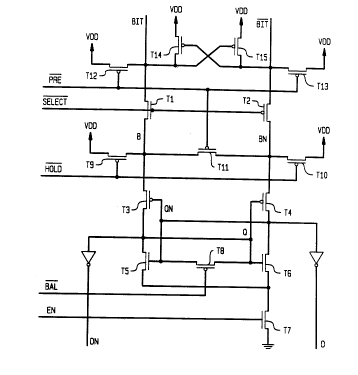
Fig. 1 i8 a schematic diagram of the sense amplifier
circuitry of the invention;
Fig. 2 shows the waveforms controlling the operation of
the circuit of Fig. 1; and
15 Fig. 3 shows the circuitry of the prior art ' 395 patent,
redrawn for purposes of comparison with the circuitry of
Fig. 1.
r~~ T. DT~.Ct~RTPTION
The circuitry of Fig. 1 will be described with
20 respect to the wave~orms shown in Fig. 2. In Fig. 2 the
convention is employed which shows the waveforms high
when in their active state. In Fig. 1 the convention is ~ ~~
employed which uses an overhead bar with the wave~orm
designation to indlcate that the waveforms is, in fact,
25 active low. Referring to the top of Fig. 1, bit lines
BIT and Brr lead to a particular memory cell (not shown)
~ ~17~7~6
of the Elame type of memory array (not shown) discussed in
the ' 395 patent .
The circuitry of Fig. 1 operates under control of
the four-phase CLOCK waveform shown in Fig. 2 ta~ which
5 controls the start and end of each of the waveforms of
Figs. 2 (b) through 2 (g) . The circuitry of Fig. 1 is
called into operation to access the memory array by the
SELECT waveform, shown in Fig. 2 (f), which remains active
throughout the following three phases labelled PRECHARGE~,
10 SENSE, and EVAL. The SELECT waveform activates
transistors T1 a~d T2 which remain conducting through the
PRECHARGE, SENSE and EVAL phases. ~ll of the transistors
in Fig. 1 are P-channel enhancement tran6istors, except
transistors T5, T6 and T7 which ar N-channel ~nhAn~ ~nt
15 transistors.
ThOE PR~T~ARlll;! p~A.C:I;!
During the PRECHARGE phase iden~if ied in Fig . 2,
waveforms PRE, Fig. 2 (b) and BAL, Fig. 2 (c), are high
(i.e., active low in Fig. 1), while waveforms EN, Fig.
20 2(e), and HOLD, Fig. 2(g), are low (i.e., inactive high
in Fig. 1) . Waveform PRE in Fig. 2 (b) activates
transistors T12 and Tl3 which initialize the bit lines to
the potential of the supply Vdd . Transistors T3 and T5
form a non-inverting amplifier for responding to the --
25 information storage state of the bit line BIT while
transistor~3 T4 and T6 form an inverter amplifier for - ---
responding to the information storage state of the bit
line BIT BAR . Transistor pair T3, T5 will hereinaf ter
sometimes be referred to as one of the pair of sense
7978~
amplifiers while transistor pair T4, T6 will be ref~erred
to as the other of the pair of sense amplifiers. During
this PRECHARGE phase, the source terminals of the
transistors T3 and T4 o both of the sense amplifiers are ~ ~~
5 connected together by balancing circult transistor T11
thereby ensuring negligible voltage difference between
these ~-rm; n~ at the end of the PRECHARGE phase.
Also during the PRECHARGE phase, the BAL waveform
shown in Fig. 2 (c) activates balance circuit transistor
10 T8 to clamp together the gate terminals of transistors
T3, T4, T5 and T6. ~Transistor T8 will remain conducting
during the subsec~uent SENSE phase, as well. ) At the same
time that the BAL waveform i8 active, the EN waveform
shown in Fig. 2 ~e) is inactive, maintaining the gate of
transistor T7 at a potential to keep this transistor in a ~=
non-conducting condition. Keeping transistor T7 non~
conducti~g isolates the sense amplifiers from ground 80
that they cannot provide a current path to gr-ound for the
bit lines. So long as transistor T7 rémains non-
20 conducting, the source t-~rm~ n~ of the transistors in
the sense amplifiers track the potential on the bit lines
but the transistors dissipate no power. During
PRECHARGE, transistors T14 and T15, which are connected
to the bit lines, are both off. These transistors will
25 come into operation when the potential of one of the bit
lines begins to fall after the termination of the
PRECHARGE interval.
-
~ ~ ~17978~
Th~ ,C~Tq~ phs~
During the SENSE phase, the BAI. waveform remains
active. The WS waveform, Fig. 2 (d), becomes active,
selecting a word line linking a column of memory cells in
5 the array (not shown, but similar to the word line
described in the ' 395 patent) . The PRE waveform of Fig.
2 (b) becomes inactive, turning off transistors T12 and
T13 and ending the PRECHARGE interval. The termlnation
of the PREC~IARGE interval allows the bit lines to assume
10 the potential dictated by the information 3tored in the
memory cell to which they are connected. The potential
of one of the bit lines will begin to fall. During this
time one of the cross-coupled sense amplifiers has its
source tracking the falling bit line but, unlike the '395
15 patent, there is no path to ground from the bit lines
through the sense amplifiers because transistor T7 i8
still in a non-conducting state. The gates of the ~- -
transIstors of the sense amp~ifiers are sti:L.l connected
together by transistor T8 under the control of the BAL
20 waveiorm. When the potential of one of the bit lines
begins to fall it, for example the bit line BIT,
transistor T14 connected to that bit line causes
transistor T15 whose drain ls connected to the opposlte
bit line to turn on, clamping that bit line high and
25 preventing both bit lines from falling.
Th ~ EY.Z~ r. ph ~ ~ "
During this phase the WS waveform remains active.
The sAL waveform becomes inactive whil~e the EN waveform
becomes active. The inactive state of the BAL waveform
~ 217~78~
renders transistor T8 non-conducting thereby ending the
balanclng of the gates of the transiGtors of the sense
amplifiers. At the same time the active phase of the EN
waveform causes transistor T7 to complete a current path
5 to ground from the bit lines through the sense
amplifiers. The sense amplifiers quickly assume the
state corresponding to the bit line that has fallen in
potential somewhat. During this phase the bit line
~-nn~1nlleq to fall as driven by the memory cell. This is
10 the only phase durlng which the sense amplifiers draw
current from any of the bit lines. The current stops
when a stable state is reached.
,Th~ T.AT~'U p,l~e
During this fourth phase, the HOLD waveform becomes
15 active, turning on translstors T9 and T10 and connecting
the sense amplifier terminals B and BN to the potential
source Vdd . This latches the data in the sense
amplifiers with no power dissipation. During this phase
the SEI~ECT waveform becomes inactive thereby turning of f
20 transistors T1 and T~ and disconnecting the memory bit
lines from the sense amplifiers. The WS waveform goes to
its inactive phase as well to save power by stopping the
memory bit line from being pulled any lower. This fourth
phase ends when the PRECHARGE ~ignal becomes active to
25 start the next cycle (or to idle the memory). The
PRECHA~GE signal can remain high until the next read
cycle begin~ when SEl~ECT rises and HODD falls.
The WRITE phase, during which information may be
entered ~nto the memory cell by circuitry (not shown
217~78~
herein, but described in the ' 395 patent~ which impresses
state-defining differential voltages on the bit lines,
may occur during or following the l,ATCH phase since the
sense amplifiers are th~ disconnected from the bit
5 lines.
Th.. Operat~--n of th~ ~395 Pat~nt r -~ed
In the '395 patent, the SELECT signal causes
transistor 58 to conduct, thereby completing a path to
ground for the bit lines through the sense amplifier3 and
10 allowing them to draw current from the bit lines
throughout the rPm~; nll~r of the memory access cycle . The
intervals tl - t2 and tz - t3 are self-timed, i.e.,
determined by analog circuit parameters. The duration of
the latter interval is determined by the voltage
15 difference between the bit lines. This period could be
quite short, unless there was little voltage difference
between the bit lines and there would be little voltage
difference if the self-timed interval, tl - t2, were -~
short. Accordingly, the shortening of one of the
2 o intervals cause~ a lengthening of the other . ~n
contrast, the circult of our i~vention allows a full
half-cycle for the SENSE phase to take place, typically
resulting in a signiiicant voltage differences. Since
our circuit allows a significant voltage difference to
25 accrue, the evaluation of the state of the bit lines by
the sense amplifiers during the EVAL phase occurs quite
rapidly. However, since the EVAL phase is not self- -
timed, the entire half-cycle of the ~VAL phase can be
devoted to allowing the sense amplifiers to settle. As
-~ 217g78~
noted above, the sense amplifiers of the '395 patent are ==
allowed to draw current throughout the tl - t~ interval
while in our circuit the sense amplifiers are permitted
to draw current from the bit lines only during the EVA~
5 phase and not during the preceding SENSE phase nor during
the succeeding I~TC~I phase.
Cnn~l 11~; nr~
What has been described is deemed to be
illustrative of the principles o my invention.
10 Numerous modi~ications may be made thereto, such altering
the start of the waveforms as indicated by the dotted
lines in Fig. 2.
other modiicatLons may be made by those skilled in the
art without, however, departing from the spirit and scope
15 oL my invention.