Note: Descriptions are shown in the official language in which they were submitted.
CA 02179790 1999-06-22
APPARATUS USING MEMORY CONTROL TAHLES RELATED
TO VIDEO GRAPHICS PROCESSING FOR TV RECEIVERS
Field of the Invention
The present invention relates to apparatus using memory
control tables in a graphics memory for processing mixed YW and
color palettized graphic video signals to produce desired special
effects. A memory controller and sprite state machine is used
with the graphics memory for selectively displaying such graphic
video signals by themselves or selectively superimposing such
mixed graphic video signals on live television signals received
from a remote source.
Backcxround of the Invention
Some commercially available computers, particularly personal
computers, provide circuitry which permits a merger of a
composite video signal, as, for example, a National Television
Standards Committee (NTSC) signal, with computer generated video
graphics display signals, typically red, green, and blue (RGB).
1
f ,
2~~9~~0
GID908
More particularly, modern videb graphite equipment has the -
ability to produce backgrounds, characters, symbols, and other
pictorial representations and arrangements in operator-selected
sizes, shapes, and colors.
U.S. Patent No. 4,737,772 (Nishi et al.), issued on April
12, 1988, discloses a video display controller comprising a video _
display processor (VDP), a Central Processing Unit (CPU), a
memory, and a Video Random Access Memory (VRAM). The memory
stores both programs to be executed by the CPU and various kinds
of image data. The VRAM stores image data which the VDP can
change and then transfer to the outside for display on a screen
of a Cathode Ray Tube (CRT) display. In the VDP, a timing signal
generator generates timing signals for correctly scanning -
elements of the picture to be displayed which are used by
horizontal and vertical counters and the CRT display to
synchronize data processing in an image data processing circuit
(IDPC) and correctly display such processed data on the screen of -
the CRT display. A Video Digitizer samples an externally
supplied analog video signal and converts signal levels or. ,
amplitudes of the analog video signal into digital data composed _
of 2 or 4 bits each. The digitized amplitude output data from
the Video Digitizer represents a still image, and the data is
supplied to the IDPC. The IDPC selectively stores both the Video
Digitizer output data and color codes supplied from the CPU in
the VRAM through an interface circuit. Each color code from the
CPU represents a color of a respective one of the display
elements (e. g. pixel) constituting a still image on the screen.
2
7 .
21~9'~9~1
GID9oa
In operation, in response to a display command from the CPU, the
IDPC sequentially reads dot data from the VRAM in synchronization
with the scanning position on the CRT display, and outputs the
dot data to a color palette circuit. Concurrently, the IDPC
calculates and reads data necessary for displaying an animation
image from the VRAM and supplies color codes to the color palette
circuit. Where an animation and still image are located at a
same display position on the screen of the CRT display, the
animation image is preferably displayed. The color palette
circuit converts each color code into three color data for red
(Rj, green (G), and blue (B), each composed of three bits. A
Digital to Analog Converter (DAC) converts the color data from
the color palette circuit into R, G, and B signals which are
provided to the CRT display.
U.S. Patent No. 5,355,175 (Okada et al.), issued on October
11, 1994, discloses video mixing apparatus that mixes a graphics
video image and a playback video image at a plurality of mixture
ratios in one image plane. Fade data indicative of the mixing
ratio of at least one line of the playback video signal and the
graphics video signal is sequentially generated in accordance
with a predetermined order. The fade data is held in holding
means and is outputted from the holding means synchronously with
a horizontal sync signal. The levels of the playback video
signal and the graphics video signal are individually adjusted in
accordance with the fade data outputted from the holding means,
and the adjusted signals are added together. The playback video
signal and the graphics video signal are mixed at the mixing
3
1
~ ~I'~9~9U
GID908
ratio set for every line on one image plane to generate a video
output signal from the apparatus.
U.S. Patent No. 4,420,770 (Rahman), issued on December 13,
1983, discloses a video background generation system for
generating rectangular video patterns having operator-selected
video attributes. The system comprises a horizontal bit memory
and a vertical bit memory, each of the memories being a 16 entity
memory for storing information for 16 background entities. The
memory for each background entity defines opposite corners of the
background area for an entity on the screen. As shown in FIG. 2
of the patent, a first entity defines a first rectangular area,
and a second higher priority entity defines a second partially
overlapping rectangular area. An attribute look-up table stores
information for each entity related to the color video output
(red, green, blue) for that entity. During the scanning of the
lines of a picture being produced, the first entity is produced
in its defined area and the second entity is produced in its
defined area. However, the second entity has a higher priority.
which results in the overlapping region of the two entities to be _
presented with the stored attributes of the second entity.
U.S. Patent No. 4,754,270 (Murauchi), issued on June 28,
1988, discloses digitized displaying apparatus which is capable
of enlarging or reducing the size of a displayed picture on the
screen of a raster scanning type display such as a CRT display.
The apparatus comprises an addressable memory means, input data
means, and variable address data generating means. The
addressable memory means stores display data that is read out in
4
1 .
~1?9'~9~
GIDSOa
a predetermined timing relationship with a raster scanning of the
display to produce a display image. The input data means
supplies numerical data that determines the size of the image.
The variable address data generating means includes variable
addressing increments for generating address data that is
correlated with display data addresses that are stored in the
memory means in order to output the display data. The variable
address data generating means comprises arithmetic calculating
means for digitally calculating addressing increments in response
to the numerical data supplied by the input data means. Still
further, in response to timing signals related to the scanning of
the display, the variable address data generating means is
responsive to the arithmetic calculating means to increment
addresses for addressing the memory means according to the
numerical data that determines the image size. More
particularly, when displaying an original sized picture, a
horizontal address of the memory means is incremented by a "1"
every 200 nanoseconds. In other words, a dot size in the
horizontal direction of the display has a 200 nanosecond
displaying time to display the original size. The dot size in
the horizontal direction can be enlarged or reduced by changing
the displaying time of one dot in the horizontal direction by
properly selecting addend data that is provided to the memory
means. By appropriate setting of the addend data, the size of
characters and the associated images on the display screen can be
enlarged or reduced with respect to a nominal size.
5
GID908
r
Presently, there is emerging a need for interactive video
graphics which will enable a whole new class of services to be
delivered to the home via a cable television network. These new
services will enhance the viewing experience for many traditional
television programs while providing augmented services to others.
However, NTSC and Phase Alternating Line (PAL) television -
receivers, unlike computer monitors, have a fairly low video
bandwidth and employ an interlaced, not a progressive scan,
display. These limitations place severe constraints on the -
generation of an artifact free high resolution synthetic video
signal. Traditionally, consumer products, such as video games,
avoid these problems by generating low resolution non-interlaced
video signals. This approach results in images that are of low
quality, have a "blocky" appearance, are limited in color choice,
i5 and take on a cartoon-like look. The generation of synthetic
video that approaches broadcast quality requires that the
generated synthesized signals emulate that of a video camera
scanning a scene and the subsequent analog signal processing for
such video camera signals. Therefore, it is desirable to provide
a relatively inexpensive arrangement that uses memory tables for
storing and processing many graphics (sprites) into various
configurations and special effects while permitting good
synthetic video graphics to be overlaid on top of each other or
live television programming for viewing on a standard NTSC or PAL
standard interlaced television receivers.
6
GID908
Summary of the Invention
The present invention is directed to inexpensive apparatus
using memory control tables for processing mixed YUV and color
palettized graphic (sprite) video-signals to produce desired
special effects, and selectively displaying such graphic video
signals by themselves or selectively superimposing such mixed
graphic video signals on live television signals received from a
remote source.
Viewed from one aspect, the present invention is directed to
apparatus for processing mixed video and graphic signals for
display on a standard television receiver comprising a graphics
memory and a memory controller and sprite state machine. The
graphics memory comprises a sprite list table, a sprite data
table, and a line control table. The sprite list table lists one -
or more graphics in a predetermined sequence for display on the
television receiver, and for storing general information related
to one or more graphics within control words in each listing.
The sprite data table stores pixel data for horizontal lines of - -
each of the one or more graphics where the horizontal lines in
the sprite data table for each of the one or more graphics is
accessed by a control word in the listing in the sprite list -
table for each of the one or more graphics. The line control
table comprising control words that are accessed by a control
word in the listing of predetermined ones of the one or more
graphics in the sprite list table. The line control table
control words for a graphic provides independent controls for
selectively relocating pixel data in each of the horizontal lines
7
t ,
~179~9~
GID908
obtained from the sprite data table to produce a predetermined
special effect for each of the predetermined ones of the one or _
more graphics. The memory controller and sprite state machine
accesses the tables of the graphics memory in a predetermined
sequence in order to assemble and display each of the one or more
graphics at predetermined locations in the horizontal lines on a
screen of -the television receiver.
Viewed from another aspect, the present invention is -
directed to apparatus for processing mixed video and graphic
signals for display on a standard television receiver comprising
a graphics memory and a memory controller and sprite state
machine. The graphics memory comprises a sprite list table, a
sprite data table, and a span list table. The sprite list table
lists one or more graphics in a predetermined sequence for
display on the television receiver and for storing general
information related to one or more graphics within control words
in each listing. The sprite data table stores pixel data for
horizontal lines of each of the one or more graphics. The
horizontal lines in the sprite data table for each of the one or
more graphics is accessed by a control word in the listing in the
sprite list table for each of the one or more graphics. The span
list table comprises at least one span list control word for a
predetermined number of horizontal lines forming each of a
plurality of predetermined separate sections of the screen of the
television receiver. The one or more span list control words
define which of a plurality of N graphic listings in the sprite
list table are active and appear in the associated predetermined
8
~Z~~~~~
GID908
section. The memory controller and sprite state machine first
accesses the at least one span Iiat control word in the span list
table when assembling a predetermined section of a screen of the
television receiver. Then, the memory controller and sprite
state machine only accesses the graphic listings in the sprite
list table and the sprite data table that are found active and
appear inthe at least one span list word.
Viewed from still another aspect, the present invention is
directed to apparatus for processing mixed video and graphic
signals for display on a standard television receiver comprising
a graphics memory and a memory controller and sprite state
machine. The graphics memory comprises a sprite list table, and
a sprite data table. The sprite list table lists one or more
graphics in a predetermined sequence for display on the
television receiver. The sprite list table also stores general
information related to the one or more graphics within control
words in each listing. The sprite data table stores pixel data
for horizontal lines of each of the one or more graphics. The
horizontal lines in the sprite data table for each of the one or
more graphics is accessed by a control word in the listing in the
sprite list table for each of the one or more graphics. The
memory controller and sprite state machine is responsive to field
enable signals from the sprite list table indicating which field
of a two-field frame of a video picture is being displayed on a
screen of the television receiver for accessing and assembling a -
first predetermined graphic listed in the sprite list table for
horizontal lines of only one of the two fields and a second
9
~
21~9~~0
GID908
predetermined graphic listed in the sprite list table or a live
television signal for horizontal lines of the other one of the
two fields.
The invention will be better understood from the following
more detailed description taken with the accompanying drawings.
Brief Description of the Drawings
FIG. 1 is a block diagram of a subscriber cable box unit in
accordance with the present invention;
FIG. 2 is a block diagram of a first portion of Video
Processing Circuitry found in the subscriber cable box unit of
FIG. 1 in accordance with the present invention;
FIG. 3 is a block diagram of a second portion of Video
Processing Circuitry found in the subscriber cable box unit of
FIG. 1 in accordance with the present invention;
FIGS. 4, 5, and 6 illustrate the operation of a Pixel
Assembly Buffer forming part of the first portion of the Video
Processing Circuitry of FIG.-3 in accordance with the present
invention;
FIG.-7 is -a block diagram of an exemplary Multiplexer/Fader
forming part of a second portion of the Video Processing
Circuitry shown in FIG. 3;
FIG. 8 is a block diagram of an exemplary arrangement of a
Convolver forming part of the second portion of the Video
Processing Circuitry shown in FIG. 3;
FIG. 9 is a block diagram of a Graphics Memory comprising
tables, and the first portion of a Video Processing Circuitry
shown in FIG. 2 in accordance with the present invention;
2I79"~90
GID908
FIGS. 10, li, 12, 13, 14, and IS show various configurations
that can be achieved using the tables of the Graphics Memory
shown in FIG. 9 in accordance with a first embodiment of the
present invention;
FIG. 16 is an exemplary view of a display screen using a
span list table found in the Graphics Memory shown in FIG. 9 in
accordance with a second embodiment of the present invention; and
FIG. 17 is an exemplary section of an interlaced television
receiver screen wherein a first and second sprite are interleaved
in a portion of the screen in accordance with a third embodiment
of the present invention.
Detailed Description
It is to be understood that corresponding elements
performing the same function in each of the figures have been
given the same designation number.
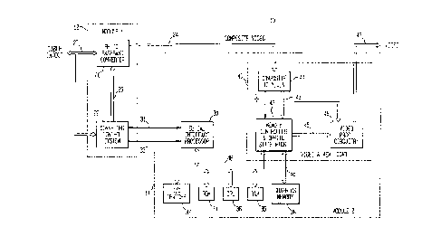
Referring now to FIG. 1, there is shown a block diagram of a
subscriber cable box unit 10 that can be found on a subscriber's
premises and provides interactive video processing in accordance
with the present invention. The subscriber cable box unit 10
comprises a first module (MODULE 1) 12 (shown within a first
dashed line rectangle) and a second module (MODULE 2) 14 (shown
within a second dashed line rectangle). The first module 12 is a
conventional arrangement that comprises a Radio Frequency (RF) to
Baseband Converter 20 and a Converter Control System 22, which
are each known in the art. The RF to Baseband Converter 20
receives multiplexed RF television channel signals in the N'fSC or
PAL standard format propagating on a cable 27 from a remote cable
11
GID908
company central office (not shown), and selectively converts such
multiplexed RF television channel signals from their multiplexed
channel frequencies to baseband frequencies: The RF to Baseband
Converter 20 transmits a resultant baseband composite video
output signal from the conversion process over a bus 24 to the
second module 14. The Converter Control System 22 is user
(subscriber) is typically controlled by either an Infra Red
remote control device or a keypad on the cable box as is well
known in the art. The Converter Control System 22 functions to
receive and/or transmit authorization and access control signals
via the cable 27 to or from a remote cable company central
office, activate baseband video scrambling or descrambling, and
produce On Screen Display (OSD) messaging. The Converter Control
System 22 outputs control signals via a bus 29 to the RF to
Baseband Converter 20 for selecting desired channel programming,
and various control and decrypted data signals (e.g., control and
upstream data output signals, Infra Red receive and transmit
signals, and decrypted T1 Quadrature Phase Shift Keying data
signals) via leads 31 and 33 to the second module 14.
The second module 14 comprises a Serial Interface Processor
(SIP) 30, Input/output (I/O) devices 32, a Read Only Memory (ROM)
34, a Random Access Memory (RAM) 35, a Central Processing Unit
(CPU) 36, a Graphics Memory 38, and a Video and Memory Control
(VIDEO & MEM. CONT.) integrated circuit 40 (shown within a dashed
line rectangle). The SIP 30, I/O devices 32, ROM 34, RAM 35, CPU
36, and a Memory Controller and Sprite State Machine (MACH.) 42
of the Video and Memory Control integrated circuit 40 are -
12
~~~~~~o
GID908
interconnected by a data bus 48. The CPU 36 can comprise any
suitable processing unit and, in accordance with the present
invention, ie a 386 type CPU which is relatively inexpensive.
The ROM 34 can comprise any suitable memory as, for example, an
EPROM for initialization purposes and for programming of the CPU
36. The RAM 35 can comprise any suitable memory as, for example,
two 256 Kilobyte-by-16 bit DRAMa connected in series to provide a
512K-by-16 bit RAM configuration for use as a scratchpad memory
for the CPU 36. The Graphics Memory 38 can comprise any suitable
memory as, for example, a 32 bit wide RAM area or preferably two
256K-by-16 bit DRAMS arranged in parallel for use with a 32-bit
wide bus 39. The Graphics Memory 38 is used to store sprite data
relating to graphics and video pictures. The use of a 32-bit
wide bus 39 permits the use of fast-page mode memory addressing
for both a Memory Controller and Sprite State Machine 42 and a
block memory mover (not shown) forming part of the Video and
Memory Controller 40. By significant use of block mode memory
addressing, an average data transfer rate of approximately 52
nanoseconds can be achieved, which corresponds to processing -
approximately 77 million bytes of data per second.
The SIP 30 functions to handle data communications between
the first module 12 and the second module 14. More particularly,
the SIP 30 handles all data transfer signals between the second
module 14 and the converter control system 22 of the first module
12. These data transfer signals can have formats such as, for
example, a T1-like data stream at 1.5 ND~its/second which involves
the bulk of the communication transfers, and raw data from an
13
21'~~~9~
GID908
infrared receiver (not shown) in the converter control system 22.
The SIP 30 can also include a full duplex-synchronous serial port
(not shown) for future expansion. Such data transfer signal
formats are used to communicate between the converter control
system 22 on the first module 12 and the CPU 36 in the second
module 14 to activate desired actions in the second module 14.
The Video and Memory Control integrated circuit 40 comprises
the Memory Controller and Sprite State Machine 42, Composite to
YUV circuitry 44, and Video Processing (PROC.) circuitry 46. The
Memory Controller and Sprite State Machine 42 is coupled to the
Graphics Memory 38 by a data bus 39, and to the Video Processing
circuitry 46 by a data bus 45. The Composite to YUV circuitry 44
receives the baseband composite video signal from the bus 24 and
outputs resultant YUV video signals to the Memory Controller and
Sprite State Machine 42 on a bus 43. The Video Processing
circuitry 46 receives video signals from the Memory Controller
and Sprite State Machine 44 over the data bus 45, and outputs
NTSC or PAL standard video signals on a bus 47 to a remote
television receiver (not shown) or further processing circuitry
(not shown). It is to be understood that the present invention
lies within the area of the Video and Memory Control integrated
circuit 40 and the Graphics Memory 38. The elements of the first
module 12 and the second module 14 were introduced and discussed
hereinbefore for a better understanding of how the present
invention fits into the interactive subscriber cable box unit 10.
Referring now to FIGS. 2 and 3, there are shown block
diagrams of first and second portions, respectively, of a Video
14
21~~~9~
GID908
Processing Circuitry 46 (shown within a dashed line area) found
in the second module 14 of the subscriber cable box unit 10 of
FIG. 1 in accordance with the present invention. As is shown in
FIG. 2, a Graphics Memory 38, forming an element of the second
module i4 of FIG. 1, is coupled via a data bus 39 to a Memory
Controller and Sprite State Machine 42 which is part of a Video
and Memory Controller 40 (shown within a dashed line area) of the
second module 14 of FIG. 1. A first portion of the Video
Processing Circuitry 46 comprises a Data Pipe 50, and a Pixel
Assembly Buffer 52 (shown within a dashed line rectangle). The
Data Pipe 50 receives data over a bus 45 that was obtained by the
Memory Controller and Sprite State Machine 42 from the Graphics
Memory 38 for a particular sprite for transmission to the Pixel
Assembly Buffer 52. More particularly, the Data Pipe 50 receives
data for a sprite from the Graphics Memory 38 via the Memory
Controller and Sprite State Machine 42 and provides separate
outputs as to luminance data (ydata) and chrominance data (cdata)
for transmission to the Pixel Assembly Buffer 52.
The Pixel Assembly Buffer 52 comprises first, second, and
third double line buffers 53, 54, and 55, respectively, and a Y/G
Line 0 buffer 58. The first double line buffer 53 is used for
storing Y/G (luminance) line la data and Y/G line 1b data for
first and second lines of a first field of a sprite picture
received via a bus 49 from the Data Pipe 50. The line luminance
data comprises 10 bits (bits 9-0) of data and control for each
pixel of a line. The second double line buffer 54 is used for
storing C (chrominance) Line la and C Line 1b data of the first
~~~~~~o
GID908
and second lines of the first field of the sprite picture
received via a bus 51 from the Data Pipe 50. The line
chrominance data comprises 8 bits (bits 7-0) of data for each
pixel of a line. The third double line buffer 55 is used for
storing Y/G (luminance) line 2a data and Y/G line 2b data of
first and second lines of a second field of a sprite picture
received via the bus 49 from the Data Pipe 50. The line -
luminance data comprises 10 bits (bits 9-0) of data and control
for each pixel of a line. It is to be understood that the Lines
1a and 2a of the first and third double line buffers 53 and 55 -
store first and second horizontal lines of pixel data,
respectively, where the first and second horizontal lines are
adjacent lines within separate fields of the sprite picture in an
interlaced display format. Similarly, Lines Ib and 2b of the
first and third double line buffers 53 and 55 store third and
fourth horizontal lines of pixel data, respectively, where the
third and fourth horizontal lines are adjacent lines within
separate fields of the sprite picture in an interlaced display
format. In other Words, the first and third double line buffers
53 and 55 sequentially store luminance data and control for, for
example, pixels of a pair of odd and even lines, respectively, of
respective first and second fields, or vice versa, of the sprite
picture during a scanning of an interlaced display format. The
second double line buffer 54 stores the chrominance data for the
data of lines stored in the double line buffer 53. A chrominance
double line buffer (not shown) similar to double line buffer 54
can be provided for double line buffer 55, but it is not
16
~1'~9'~9~
GID908
necessary for reasons of economy and unimportance in a Convolver
that will be explained hereinafter. The output data from the
first double line buffer 53 comprises ten bits of luminance data
and control for each pixel of the lines stored therein which is
outputted in parallel for each pixel over a bus designated LINE 1
to circuitry in FIG. 3. The output data from the second double
line buffer 54 comprises eight bits of chrominance data for each
pixel of the lines stored therein which is outputted in parallel -
for each pixel over a bus designated LINE 1c to circuitry in FIG.
3. The output data from the third double line buffer 55
comprises ten bits of luminance data and control for each pixel
of the lines stored therein which is outputted in parallel for
each pixel over a bus designated LINE 2 to circuitry in FIG. 3
and to the Y/G Line 0 Buffer 58. The Y/G Line 0 Buffer 58
functions to delay the line data outputted by the third double
line buffer 55 by one horizontal line period to provide a delayed
line output comprising ten bits of luminance data and control for
each pixel of the line stored therein which is outputted in
parallel over a bus designated LINE 0 to circuitry in FIG. 3. It
is to be understood that at a sampling rate of 13.5 Mfiz for the
NTSC standard television display, there are 858 pixels per line _
of the picture of which only about 704 pixels are actually
displayed, and that there are 525 horizontal lines of pixels in
two fields of a picture of which about 440-500 lines are normally
seen depending on the television receiver used.
Turning now to FIGS. 4, 5, and 6, there is shown an
exemplary sequence of operation for the first and third double
17
2179 790 GID908
line buffers 53 and 55, respectively, and the Y/G Line 0 Buffer -
58 of the Pixel Assembly Buffer 52 of FIG. 2 in accordance with
the present invention. It is to be understood that in a normal
operation of the double line buffers 53 and 55, a horizontal line
of pixel data in a first field is inputted to one half of the
first double line buffer 53 concurrent with a horizontal line of
pixel data in a second field being inputted to one half of the
third double line buffer 55.- Concurrent with the inputting of
horizontal lines of pixel data into first halves of the first and
third double line buffers 53 and 55, horizontal lines of pixel
data previously stored in the other halves of the first and third
double line buffers 53 and 55 are read out on output LINES 1 and
2, respectively. In other words, for the first double line
buffer 53, a first horizontal line of pixel data from the first
field is inputted to, for example, the Y/G LINE 1a portion of the
first double line buffer 53, and during a next horizontal line
period a second horizontal line of pixel data from a first field
of a frame is inputted to the Y/G LINE lb portion of the first
double line buffer 53 while the first horizontal line of pixel -
data from the Y/G LINE Ia portion is read out onto output LINE 1.
During a next horizontal line period, a third horizontal line of
pixel data from the first field is inputted to the Y/G LINE la
portion of the first double line buffer 53 while the second
horizontal line of pixel data from the Y/G LINE 1b portion is
read out onto output LINE 1. Concurrently, first, second, and
third horizontal lines of pixel data from a second field of the
18
CA 02179790 1999-06-22
frame are similarly read into the third double line buffer 55 and
outputted therefrom onto output LINE 2.
FIG. 4 shows an end point of an initialization stage of the
Pixel Assembly Bufi:er 52 after the subscriber cable box unit 10
of FIG. 1 is first turned on. More particularly, on turn on,
pixel data for a horizontal line 0 of a first field and pixel
data for a horizontal line 1 of a second field are inputted to
the Y/G line 1a portion of the first double line buffer 53 and
the Y/G line 2a portion of the double line buffer 55,
respectively, during a first horizontal line period. During a
second horizontal line period, pixel data for a horizontal line 2
of a first field and pixel data for a horizontal line 3 of a
second field are inputted to the Y/G line lb portion of the first
double line buffer 53 and the Y/G line 2b portion of the third
double line buffer :55, respectively, while the pixel data for
horizontal lines 0 and 1 are read out of Y/G line la portion of
the first double line buffer 53 and the Y/G line 2a portion of
the third double line buffer 55, respectively, on respective
output LINES 1 and :?. Concurrent therewith, the pixel data for a
horizontal line 1 f~.°om the Y/G line 2a portion of the third
double line buffer 55 is inputted to Y/G Line 0 Buffer 58. Since
the Y/G Line 0 Buffer 55 functions to delay horizontal line data
stored therein by one horizontal line period, and the Buffer 58
had no data stored therein upon initialization, the output
therefrom on output LINE 0 includes no valid data.
FIG. 5 continue, the loading and outputting process after
the initialization steps shown in FIG. 4. More particularly,
19
2179~~~
GID908
pixel data for a horizontal line 4 of a first field and pixel
data for a horizontal line 5 of a second field are inputted to
the Y/G line la portion of the first double line buffer 53 and
the Y/G line 2a portion of the third double line buffer 55,
respectively, during a third horizontal line period. Concurrent
therewith, the pixel data for the horizontal lines 2 and 3 are
read out of-Y/G line 1b portion of the first double line buffer'
53 and the Y/G line 2b portion of the third double line buffer
55, respectively, on their respective output LINES 1 and 2.
i0 Concurrent therewith, the pixel data for the horizontal line 3
from the Y/G line 2b portion of the third double line buffer 55
is inputted to Y/G Line 0 Buffer 58 while the previously stored
pixel data for the horizontal line 1 data is outputted on output
LINE 0. Therefore, the Buffers 58, 53, and 55 are outputting
pixel-data for the horizontal lines 1, 2, and 3, respectively,
for a sprite on respective output LINES 0, 1, and 2 during the
third horizontal line period, where the pixel data for the
horizontal lines 1 and 3 are part of the second field and the
pixel data for the horizontal line 2 is part of the first field
of a sprite picture that were stored in the Graphics Memory 38
(shown in FIGS. 1 and 2).
FIG. 6 continues the loading and outputting process from the
step shown in FIG. 5. More particularly, pixel data for a
horizontal line 6 of a first field and pixel data for a
horizontal line 7 of a second field of a sprite are inputted to
the Y/G horizontal line 1b portion of the first-double line
buffer 53 and the Y/G horizontal line 2b portion of the third
~1'~9'~90
GID908
double line buffer 55, respectively, during a fourth horizontal
line period. Concurrent therewith, the pixel data for the
horizontal lines 4 and 5 of the sprite are read out of Y/G
horizontal line 1a portion of the first double line buffer 53 and
the Y/G horizontal line 2a portion of the third double line
buffer 55, respectively, on respective output LINES 1 and 2.
Concurrent therewith, the pixel data for the horizontal line 5
from the Y/G line 2a portion of the third double line buffer 55
is inputted to Y/G Line 0 Buffer 58 while the previously stored
pixel data for the horizontal line 3 data is outputted on output
LINE 0. Therefore, the Buffers 58, 53, and 55 are outputting
pixel data for the horizontal lines 3, 4, and 5, respectively, on
respective output LINES 0, 1, and 2 during the fourth horizontal
line period, where the data for the horizontal lines 3 and 5 are
part of the second field-of the sprite picture while the data for
the horizontal line 4 is obtained from the first field of the
sprite picture that were stored in the Graphics Memory 38 (shown
in FIGS. 1 and 2). From FIGS. 5 and 6, it can be seen that after
initialization (FIG. 4), the pixel data on the output LINE 1
represents data for sequential horizontal lines (e. g., even
numbered horizontal lines (0-254) of an NTSC standard picture) of
a first field of the two fields of a frame for an NTSC interlaced
display. After the exemplary even numbered horizontal lines of
the first field have been sequentially outputted on the output
LINE 1 during sequential horizontal line periods, the output
continues with sequentially numbered horizontal lines (e.g., odd
numbered horizontal lines 1-255 of an NTSC standard picture) of
21
~1~9790
GID908
the second field of the frame in the manner found for scanning an
interlaced display. Although not shown in FIGS. 4-6, it is to be
understood that the chrominance data is outputted on output LINE
1c from the second double line buffer 54 shown in FIG. 2,
concurrent with the associated luminance pixel data for each
horizontal line being outputted on output LINE 1 .
Turning now to FIG. 3, there is shown a block diagram of a
second portion of a Video Processing Circuitry 46 found in the
subscriber cable box unit 10 of FIG. 1 in accordance with the
present invention. The second portion of the Video Processing
Circuitry 46 comprises Color Palette circuitry 60, a YC to YW
Demultiplexer 62, a Multiplexer/Fader (MLTX./FADER) 64, a 3:1
Multiplexer and Control (3:1 MUX. & CONT.) 66, and a Convolver
68. The 10-bit pixel data (bits 9:0) propagating on each of
LINES 0, 1, 2 from the output of the Pixel Assembly Buffer 52 of
FIG. 2 for corresponding pixels in three adjacent horizontal
lines of a sprite picture are received at separate inputs of each
of the Color Palette circuitry 60, the YC to Y~7V Demultiplexer 62
and the 3:1 Multiplexer and Control 66. More particularly, bits
7-0 of the parallel 10-bit/pixel output from the Pixel Assembly
Buffer 52 for each of output LINES 0, 1, and 2 are received at
the inputs of the Color Palette circuitry 60 and the YC to YW
Demultiplexer 62, while bits 9 and 8 of the parallel IO-bit/pixel
output from the Pixel Assembly Buffer 52 for each of output LINES
0, 1, and 2 are received at the inputs of the 3:1 Multiplexer and
Control 66. Additionally, the YC to YW Demultiplexer 62
receives the chrominance data bits 7-0 outputted in parallel on
22
21°~~'~90
GID908
output LINE lc from the Pixel Assembly Buffer 52 since the
chrominance data is only used when the sprite pixel data relates
to a True Color sprite signal. More particularly, where sprite
data is encoded as a color palette signal, the code itself
defines the color, and chrominance data is not required as is
needed with a true color video signal.
The Color Palette circuitry 60 functions to detect when the
8 bits (bits 7:0) of parallel received pixel data on each of
output LINES 0, 1, and 2 represent separate codes for particular
colors of a color palette, and to convert those color palette
codes into an output signal on bus 61 representing a 24-bit YUV
multiplexed color palette signal for three 8-bit pixel data
received for those three lines. Color Palette circuitry 60 is a
well known device, and any suitable circuit can be used therefor.
The YC to YUV Demultiplexer 62 detects when 8 bits (bits 7:0) of
parallel received data for pixels on each of the output LINES 0,
1, and 2 from the Pixel Assembly Buffer 52 represents true color
data (e. g., a sprite obtained directly from a television
picture), and also uses the 8-bit chrominance data obtained via
output LINE 1c from the Pixel Assembly Buffer 52 to generate a
24-bit True Color YW output signal for pixels of the three lines
for transmission on bus 63.
The Multiplexer/Fader (MUX./FADER) 64 receives, at separate
inputs thereof, each of the 24-bit color palette YW data signals
propagating on a bus 61 from the Color Palette circuitry 60, the
24-bit true color YW data signals propagating on bus 63 from the
YC to YW Demultiplexer 62, and 24-bit YW live video signals on
23
21~~~90
GID908
a bus 59. The Multiplexer/Fader 64 is responsive to control
signals on a lead 67 from the 3:1 Multiplexer and Control 66 to
output one of the three input signals (24-bit color palette YUV,
24-bit true color YUV, or 24-bit live video YUV) received at the
Multiplexer/Fader 64 during each pixel period as digitized YUV
mixed output signals on a bus 65. More particularly, the 3:1
Multiplexer and Control 66 determines from the bits 9 and S
received on the output LINES 0, 1, and 2 from the Pixel Assembly
Buffer 52 whether the pixel data from the Pixel Assembly Buffer
52 on the output LINES 0, 1, and 2 represents color palette data,
true color data, or data (non-valid data) for a pixel that is not
part of a sprite to be overlaid on a live video signal, and,
therefore, the live video signal should be used for that pixel
instead of the color palette or true color data received from the _
Pixel Assembly Buffer 52. As a result of such control
information obtained from bits 9 and 8 of output LINES 0, l, and
2 from the Pixel Assembly Buffer 52, the 3:1 Multiplexer and
Control 66 sends control signals over the lead 67 to the
Multiplexer/Fader 64 to select the correct input data for each
pixel of a picture to be displayed on a remote NTSC or PAL
television receiver (not shown). The Convolver 68 uses
sequential sets of three pixel data values received in the signal
from the Multiplexer/Fader 64 on bus 65 to provide an 8-bit
weighted output signal for pixel data for a central pixel in a 3-
by-3 matrix of corresponding pixels in three adjacent lines of a
television picture or provide the signal from the
Multiplexer/Fader 64 on bus 65 as a YUV output signal on bus 47
24
21~9~9G
GID908
depending on control signals from the 3:1 Multiplexer and Control
66 over a lead 69.
Referring now to FIG. 7, there is shown a block diagram of
an exemplary Multiplexer/Fader circuit 64 (shown within a dashed
line rectangle) which comprises a 2:1 Multiplexer (MUX.) 72, and
a Fader 74 (shown within a dashed line rectangle). The Fader 74
comprises an A-B Adder 75, a Signed Multiplier (SIGNED MULT.) 77,
and an A+B Adder 78. The 2:1 Multiplexer receives each of the
Graphic data signals from the Color Palette 60 on bus 61 at a
first input terminal (A), and the Graphic data signals from the
YC to YUV Demultiplexer 62 on bus 63 at a second input terminal
(B). A control signal on lead 67 from the 3:1 Multiplexer and
Control 66 selects which of the two Graphic input signals (from
input terminal A or B) will be output from the 2:1 Multiplexer 72
at output terminal (O). Pixel Graphic output signals (Y, U, or
V) from an output terminal (O) of the 2:1 Multiplexer 72
(designated G) on a bus 70 are received at a first input terminal
(A) of the A-B Adder 75 of the Fader 74. A live video YW signal
(Y, U, or V) (designated L) is received from a bus 59 at a second
input terminal (B) of the A-B Adder 75. The pixel data values of
the A terminal input data from the 2:1 Multiplexer 72 less the
data values of the live video YUV pixel data received the B input
terminal is provided as an output at an output terminal (O) of
the A-B adder 75. The Signed Multiplier 77 receives from, for
example, a register (not shown) a 9-bit changeable ratio control
value (R) on a bus 71 at a first input ternLinal (A), and the
output from the A-B Adder 75 on a bus 76 at a second input
~
21°~9'~90
GID908
terminal (B). The resultant multiplied value of the ratio
control value (R) on the bus 71 and the Graphic signal output
data from the A-H Adder 75 on the bus 76 is output at an output
terminal (0) on a bus 79 to a first input terminal (A) of the A+B
Adder 78. The live video signal (Y, U, or V) on bus 59 is
received at a second input terminal (B) of A+B Adder 78, and the -
sum of the two input signal values are provided as a output
signal (designated Q) on the bus 65 to the Convolver 68 (shown in
FIG. 3).
The Fader 74 functions to fade a graphic signal for a sprite
in or out so that the graphic does not appear or disappear
instantaneously over the live a video signal. In other words,
for a graphic fade-in, the Fader 74 causes the graphic to appear
with increasing intensity on a television receiver while the live
video signal decreases in intensity in the area of the graphic -
over a short period of time so that the graphic is totally
visible. Similarly, for a graphic fade-out, the Fader 74 causes
the graphic to appear with decreasing intensity on a television
receiver while the live video signal increases in intensity in
the area of the graphic over a short period of time until the
graphic disappears. The operation of the Fader 74 can be
explained in accordance with the following algorithms. For the
following, an exemplary 9-bit fade multiplier (R) bus 71 is
defined as follows. Prom the above definitions, R is the fade
control value and ranges from 0 to 256.
Q = [(R/256)*G] + [(1-R/256)*L), and
= L + [(G-L)*R]/256, Eq. 1
26
2179~9Q
GID908
where "L" is a pixel value of the live video, "G" is a pixel
value of the sprite overlay, and the symbol '«" represents a
multiplying function. From Equation 1 above, as the ratio used
for the multiplying value R changes, the intensity of the graphic
and live video signals change in a opposite directions.
Referring now to FIG. 8, there is shown a block diagram of
the Convolver 68 shown in FIG. 3. The Convolver 68 (shown within
a dashed line rectangle) comprises a Bypass circuit 80, a
convolver circuit 82, and a Multiplexer (MUX.) 84. The Bypass
circuit 80 receives sequential pixel data from the
Multiplexer/Fader 64 (shown in FIGS. 3 and 7) on bus 65, and
concurrently generates therefrom data on buses 81 for three
pixels in a vertical of a sprite to be displayed on a television
receiver. More particularly, the three pixels are obtained from
corresponding pixels in three adjacent lines of both fields of a
frame making up a sprite picture. The three pixel data values
are obtained by any suitable arrangement such as a plurality of
delay circuits operating from a pixel clock or a three times
pixel clock. The three pixel data values are received via buses
81 by the Convolver circuit 82. The sequential pixel data from
the Multiplexer/Fader 64 is received by the Bypass circuit 80 on
bus 65. The sequential pixel data from the Multiplexer/Fader 64
passes through the Bypass circuit 80 and is provided to a first
input (A) of the Multiplexer 84 via a bus 85. Still further, the
Bypass circuit 80 transmits sequential sets of three pixel data
values from separate outputs thereof to separate inputs of the
Convolver circuit 82 on buses 81. The Convolver circuit 82
27
CA 02179790 1999-06-22
provides an 8-bit weighted output signal for pixel data for a
central pixel in a 3-by-3 matrix of corresponding pixels in three
adjacent lines of a television picture to a second input (B) of
the Multiplexes 84 via a bus 86. The Multiplexes 84 selects the
signals at the first (A) or second (B) inputs for transmission to
the output terminal. (0) and bus 47 depending on control signals
from the 3:1 Multiplexes and Control 66 over a lead 69.
The Convolver circuit 82 effectively multiplies (using just
adders and delays) the three pixels of a vertical received on
buses 81 in a 3-by-3 matrix of pixels with predetermined weight
values, and provides an averaged output signal for the central
pixel of the 3-by-3 matrix to a second input (B) of the
Multiplexes 84. This process continues for each pixel of a
central row (output LINE 1 of the Pixel Assembly Buffer 52 of
FIG. 2) as the sprii~e data for the corresponding pixels of the
three adjacent line:a as the pixel data progresses (shifts)
horizontally across the sprite picture for three adjacent lines.
Referring now t:o FIG. 9, there is shown a Graphics Memory
38, and a portion of: the Video Processing Circuitry 46 (shown
within a dashed line; rectangle) as is shown in FIG. 2 forming
part of a Video and Memory Controller 40 of the second module 14
of FIG. 1. The Graphics Memory 38 is coupled via a data bus 39
to a Memory Controller and Sprite State Machine 42 forming part
of the portion of the Video Processing Circuitry 46 for
28
21~9~90
GID908
bidirectional communication. The Memory Controller and Sprite
State Machine 42 is coupled to a Central Processing Unit (CPU) 36
(shown in FIG. 1) via a bus 48 for writing into the Graphics
Memory 38 via the bus 39, and receives Field <1:0> signals from
the Composite To Y,U,V circuitry 44 of FIG. 1 via conductor 56.
This portion of the Video Processing Circuitry 46 further
comprises a Data Pipe 50 (shown within a dashed-line rectangle),
and a Pixel Assembly Buffer 52.
The Data Pipe 50 comprises a Pixel Buffer Address Generator
97 and a Pixel Buffer Data Pipe 98 which each receive an output
signal from the Memory Controller and Sprite State Machine 42 via
a bus 45. The Pixel Buffer Address Generator 97 and the Pixel
Buffer Data Pipe 98 transmit separate address and pixel data
output signals, respectively, to the Pixel Assembly Buffer 52 via
respective buses 49 and 5i. The Pixel Buffer Data Pipe 98 also
receives the data on bus 39 directly from the Graphics Memory 38.
The Pixel Buffer Address Generator 97 and the Pixel Buffer Data
Pipe 98 use pixel data obtained from a Sprite Control word in a
Sprite Entry, a Sprite Data table 92, and any other information
from a Line Control table 94 in the Graphics Memory 38 to place
the data for each pixel in the appropriate address location of
the Double Line Buffers 53, 54, and 55 (shown only in FIG. 2) of
the Pixel Assembly Buffer 52. As will be explained in more
detail hereinafter, special effects like magnification, warping,
etc. for horizontal lines of a Sprite Entry are obtained from the
Sprite Control words in the associated Sprite Entry and from the
Line Control table 94 of the Graphics Memory 38. The Pixel
29
~1~9790
GID908
Buffer Address Generator 97 of the Data Pipe 50 uses this
information to appropriately alter the pixel address in a line of -
sprite data obtained from the Sprite Data table 92 of the
Graphics Memory 38 to achieve the designated special effect.
This altered address is sent to the Pixel Assembly Buffer 52 for
use in placing the associated pixel data in the pixel location
designated by the altered address in the Double Line Buffer 53,
54, or 55 of the Pixel Assembly Buffer 52 to subsequently provide
the designated special effect on the television screen. The
Pixel Buffer Data Pipe 98 concurrently receives the pixel data
for the pixel address, and transmits the pixel data to the Pixel ...
Assembly Buffer 52 for storage at the address of the Double Line
Buffer 53, 54, or 55 generated by the Pixel Buffer Address
Generator 97. The Pixel Assembly Buffer outputs luminance pixel
I5 data for three adjacent horizontal lines of a sprite one buses
designated LINE 0, LINE I, and LINE 2, and outputs chrominance
pixel data associated with the LINE i luminance output data on a
LINE 1c as was explained hereinbefore for the Pixel Assembly
Buffer in FIG. 2.
The Graphics Memory 38 comprises multiple Tables comprising
the Sprite Liat table 90, the Sprite Data table 92; the Line
Control table 94, and a Span List table 96. The Sprite List
table 90 comprises a separate memory section for each of one or a
plurality of N sprites (only entries for sprites #1, #2, and #N
are listed). As is shown for the Sprite #1 entry, the memory
section therefor comprises a Sprite Data Pointer portion, a
Sprite Controls portion, a Line Table Pointer portion, an Other
21~9~90
GID908
Optional Controls portion, and a Field Enable Control portion.
The Sprite Data Pointer portion is used to access the Sprite Data
Table 92 at a predetermined location associated with the Sprite
Entry. The Sprite Controls portion comprises data relating to,
for example, the size of the sprite, its X and Y location or
position on the screen of the television receiver, and
information about magnification, warping, etc. that is to be
performed on the sprite. More particularly, if the Sprite
Controls portion indicates that a sprite has a magnification of
2, then every line of the sprite is magnified by 2. Similarly,
if the Sprite Controls portion indicates that a sprite hae an
offset of 2, then all lines of the sprite are offset by 2. The
Sprite Controls portion affects each horizontal line of pixel
data of the sprite the same way.
The Line Table Pointer portion of each Sprite Entry is used
to access a predetermined portion of the Line Control Table 94
for control words associated with that Sprite Entry in order to
produce more advanced special effects from that produced by the
Sprite Controls portion discussed above. Finally, the Field
Enable Control portion is used to produce ~~smoked glass~~
(transparent overlay) effects on the screen of the television
receiver for the Sprite Entry being accessed in the Sprite Liat
table 90. Similar portions are shown for each of the other
sprite #2 to #N entries. Still further, the sprites in the
Sprite List table 90 are preferably listed in order of increasing -
priority where, for example, the sprite #1 entry has a lowest
priority and the sprite #N entry has a highest priority. As a
31
r ~a~9~~~
GID908
result of such priority arrangement, pixels of a sprite with a
higher priority overwrite, replace, or take precedence over
pixels of a sprite with a lower priority where two sprites or a
sprite and live video are located in an overlapping location on a
screen of a television receiver.
The Sprite Data table 92 comprises data words including pure
data for each of the pixels of each horizontal line for each
Sprite Entry of the Sprite List table 90. In other words, when a
Sprite Entry is accessed in the Sprite List table 90, the Sprite
Data Pointer portion directs the access into the Sprite Data
table 92 where the Sprite Data words (e.g., Sprite A Data word to
Sprite C Data word) for that Sprite Entry are stored in the
Sprite Data table 92 of the Graphics Memory 38. It is to be
understood that these Sprite Data words do not include the
numerical number of lines in the sprite since the size of the
sprite, the location on the screen of the television receiver,
etc., for that sprite is located in the Sprite Controls portion
of the Sprite List Entry. The Sprite List table 90 and the _.
Sprite. Data table 92 work together by first accessing The Sprite
List table 90 and then, under control of the Sprite Data Pointer
portion, accessing the Sprite Data table 92 to retrieve the data
that tells the Video Processing Circuitry 46 to draw the sprite
in the manner described by the Sprite Data words.
The Line Control Table 94 of the Graphics Memory 38 is an
optionally used table that contains subtables of separate
predetermined lengths (only one subtable is shown including N
control words), where each subtable comprises a separate line
32
~~~9~~~
1
GID908
control word for each line of a sprite. The line control words
in the Line Control Table 94 provide independent controls for the -
lines of that sprite. More particularly, as stated hereinabove,
the Sprite Controls portion of each Sprite Entry in the Sprite
List table 90 affect every line of a sprite in the same manner.
In contrast, the Line Control Words in a aubtable in the Line
Control Table 94 for a Sprite Entry, as pointed to by the Line
Table Pointer portion of the Sprite List table 90, are used to
provide independent controls for each of the lines of that
sprite. For example, it is assumed that the Sprite Controls
portion for the Sprite #1 Entry indicates that the Sprite #1
image includes ten lines at a location X and Y on the screen of
the television receiver without any special effects such as
constant offsets. The pixel data for each of the ten lines of
the Sprite #1 image is provided in the Sprite Data table 92
beginning at the address therein indicated by the Sprite Data
Pointer portion of the Sprite #1 Entry. Special effects that
might be used for any one or more of the ten lines of Sprite #1
are found in certain ones of the line control words in the Line -.
Control Table 94 beginning at the address indicated by the Line
Table Pointer portion of the Sprite #1 Entry. In other words,
the edges of the image of Sprite #1 might be aligned in a
straight line on the screen of the television receiver. However;
with the line control words of the Line Control Table 94, each
line of Sprite #1 Entry can have, for example, different offsets
for warping the image in a predetermined manner. For example, a
sprite image can be warped using the associated line control -_
33
21'~9~90
GID908
words Line Control table 94 to appear on the outside surface of a
three-dimensional cylinder.
Referring now to FIGS. 10, 11, I2, i3, 14, and 15, there axe
shown examples of what can be done with the line control words of
the Line Control table 94 in accordance with a first embodiment
of the present invention. More particularly, in FIG. 10 there is
shown a sprite image as defined by both the Sprite Controls of
the Sprite List table 90 and the sprite data associated with a
Sprite Entry in the Sprite Data table 92 without any advanced
special effects as may be introduced via a subtable in the Line
Control table 94. In FIGS. 11 and 12 there are shown how the
sprite image of FIG. 10 can be changed to produce pseudo three
dimensional effects by varying horizontal offsets on each line. a
For example, in FIGS. 11 and 12 each line of the sprite of FIG. T
10 is offset by separate amount as defined in the line control
words of a first and second subtable, respectively, of the Line
Control Table 94.
FIG. 13 shows an example of performing an advanced warping ,-
effect with horizontal magnification line controls on the sprite
image of FIG. 10. More particularly, the line control words of a
subtable of the Line Control Table 94, as pointed to by the Line
Table Pointer of a Sprite Entry of the Sprite List table 90,
defines both the amount of warping or offsetting for each edge of
the sprite for each line of the sprite, and the amount of -
magnification to be used for each line of the sprite.
FIGS. 14 and 15 show an example of an advanced special
effect of varying horizontal line mirroring on each line of a
34
21~9'~90
GID908
sprite. More particularly, FIG. 14 shows a sprite image as may
be defined by an associated Sprite Entry of the Sprite List table
90 and the Sprite Data table 92. FIG. 15 shows how a subtable of -
the Line Control Table 94 can change the sprite image of FIG. 14
by varying horizontal line offsets in only the top half of the
sprite image to produce a mirror image of the bottom half of the
sprite image shown in FIG. 14. Other advanced special effects
that can be performed with subtables of the Line Control Table 94
are, for example, (a) varying a color palette bank for 256 colors
in a 4-bit sprite; (b) varying visibility control for making -
selective lines of a sprite image disappear, and (c) varying
horizontal clipping limits for selectively clipping around a
shape of a sprite image. An advantage obtained by the use of the
Line Control Table 94 ie that an advanced special effect created
by a particular subtable can be used by many of the Sprite
Entries in the Sprite Liat table 90. This saves memory space in
contrast to building the aubtable into each of the Sprite-Entries
as may be found in the prior art. Still further, data far a same-
sprite image can be used in multiple Sprite Entries of the Sprite
List table 90, where each of the multiple Sprite Entries uses its
Line Table Pointer portion to enter a different subtable of the
Line Control Table 94. Such multiple same Sprite Entries
associated with different Line Control subtables is used where a
same sprite image with different advanced special effects is to
be seen at different locations on the screen of the television
receiver.
2~'~9'~9Q
GIDSOa -
Returning now to FIG. 9, the Span List table 96 is an
optional table which is used to save time in processing many
Sprite Entries in the Sprite List table 90. In prior art
systems, each of the Sprite Entries in a Sprite List table 90 are
sequentially entered to determine if that sprite exists in a
pixel being assembled for a horizontal line using the size and
the X and Y location on a display screen designated for that
sprite. As a result, the prior art systems, for example, for
playing games were limited to a few number of sprites (e.g., N=8
or 16 sprites) in order to assemble the pixels for each line
within the time period necessary for displaying such horizontal
line on the display screen.
In the present subscriber cable box unit 10, without the
optional Span List table 96 being present, the Memory Controller
and Sprite State Machine 42 normally accesses each of the
plurality of N Sprite Entries listed in the Sprite List table 90
of the Graphics Memory 38 to determine which of the N Sprite
Entries exist in each pixel of the horizontal line being
assembled. In accessing each of the N Sprite Entries of the
Sprite List table 90, the Memory Controller and Sprite State
Machine 42 obtains the data from the Sprite Data table 92 and the
optional Line Control Table 94 needed for each sprite to produce
the pixel data for each horizontal line being assembled in the
Pixel Assembly Buffer 52. However, if the Memory Controller and
Sprite State Machine 42 has to access and process, for example,
96 different Sprite Entries, the time necessary to process the 96
sprites would exceed a time period permitted for assembling each
36
?1~~~~~
GzD9oa
horizontal line of pixel data in the Pixel Assembly Buffer 52.
The use of the Span Liat table 96 overcomes this problem.
Where the optional Span List table 96 is used, at least one
register (not shown) in the Memory Controller and Sprite State
Machine 42 indicates that the Span List table 96 exists, and
provides all of the data necessary for the Memory Controller and
Sprite State Machine 42 to properly use the Span List Table 96,
including a portion designated "# Sprite Entry Words" which
contains a number (integer value) of words (NW) per Sprite List
Entry which is a constant integer value for each of the Sprite
Entries when the Span List table 96 exists. More particularly,
each Sprite Entry in the Sprite List table 90 can include words
for (1) a Sprite Data Pointer, (2) Sprite Controls, (3) an
optional Line Table Pointer word, (4) an optional word for
optional sprite controls, and (5) an optional Field Enable
Control Word. Therefore, in theory, each Sprite Entry of the
Sprite List table 90 can contain from 2-5 words. When a Span
List table 96 is used, each of the Sprite Entries of the Sprite
List 90 includes a same number of words (e. g., 5 words)
regardless of what optional words are normally required for each
Sprite Entry. The purpose of the register which indicates the
Number of Sprite Entry Words in each Sprite Entry is to simplify
accessing of only certain ones of the Sprite Entries of the
Sprite List table 90 when building the pixels of a horizontal
line.
The Span List table 96 comprises one span list control word
or a group of span list control words that describe which of the
37
. . ~1~9°~9f~
GID908
N sprites found in the Sprite List table 90 exist in each line.
It is to be understood that the Span List table 96 is primarily
used where there are many sprites (e. g., N=96 sprites) in order
to reduce processing time in assembling the pixel data for each
of the horizontal lines in the Pixel Assembly Buffer 52. The
number of words in the Span List table 96 is dependent on the
Equation
No. of span List worse ~ (NS/32)*(NH/NL), Eq. 2
where NS is the number of total sprites on the display screen, NH
is the.number of lines in the display screen, NL is the number of-
lines on the screen of a television receiver per span list word,
and 32 represents the exemplary number of bits available in each
word of the Span Liat table 96. The values for NH and NL are
programmable numbers, and NL can have a value of, for example, 2,
4, 8, 16, 32, 64, or 128. More particularly, although there
electrically are 525 horizontal lines of video in two fields of a
standard NTSC television display, only about 440-500 lines are
normally seen depending on the television receiver used. The
display area of the screen where the 96 sprites are to displayed
can vary from 0-500 lines for any predetermined number of
sections, where each section has an equal number (NL) of lines.
Referring now to FIG.- 16, there is shown a portion of video -.
display screen that is divided by dashed lines into 4 equal
sections 110, 111, 112, and 113 with each section having an
exemplary number of 32 lines per span list word (NL) in
accordance with a second embodiment of the present invention.
Therefore, the overall area of the video display screen that is
38
GID908
used to display the exemplary 96 sprites covers 128 horizontal
lines (4 sections at 32 linea/section). Still further, there is
shown a plurality of sprite images, where predetermined ones of
the various sprite images are designated 101, 102, 104, 106, 108,
and 109, which for purposes of discussion hereinbelow will
represent Sprite Entries 1, 2, 4, 6, 8, and 9, respectively, in
the Sprite List table 90. In accordance with Equation (2), the
number of Span List words is equal to (96 sprites/32) times (128
lines in the display screen (NH) divided by 32 lines per span
list word (NL)) which results in a total of 3*4=12 span list
words. More particularly, the first three Span List words are
associated with section 110 of the video display screen area, the
next three Span List words are associated with section 111, the
next three Span List words are associated with section 112, and
the last three Span List words are associated with section 113
for a total of twelve Span List words.
As is shown in Section 110 of the display screen area, only
the Sprite Entries numbered i, 2, 4, and 6 of the Sprite List
Table 90 are found on any of the 32 lines of the display screen
being assembled in the Pixel Assembly Buffer 52 shown in FIG. 9.
Therefore, a first 32-bit word in the Span List Table 96
associated with section 110 have the 32 bits appears as,
00000000000000000000000000101011,
where the right-most bit is associated with Sprite #1 Entry and
the left-most bit is associated with Sprite #32 Entry in the Span
List table 90 of the Graphics Memory 38. Still further, the
°°ls°°
in the Span List word indicate that sprites 1', 2, 4, and 6 are
39
GID908
active in section 110. The remaining second and third words in
the Span Liat table 96 associated with section 110 for sprites
33-96 each contain 32 zeros since none of these Sprites Entries
in the Sprite Liat table 90 are active or appear in section 110.
The other nine Span List words associated with sections 111-113
are coded in the same manner for the sprites active or appearing
in each of these sections.
In operation, the Memory Controller and Sprite State Machine
42 of FIG. 9 determines from the one or more registers therein
that a Span List table 96 exists, also obtains the data (NS, NH,
and NL values, the start line for the display area, and the
number of sprites) that is stored therein and needed for use with
the Span List table 96, and determines the number of Span List
words needed for each section of the display area in accordance
with Equation (2). In assembling the pixel data for the 525
lines of the video display, when the Memory Controller and Sprite
State Machine 42 reaches the start line for the Span List display
area the Memory Controller and Sprite State Machine 42 first.
accesses the Span List words (e. g., first three words) associated
with the top section (e. g., section 110) of the span list display
area. From these first three words of Span List table 96, the
Memory Controller and Sprite State Machine 42 determines that
only Sprite Entries 1, 2, 4, and 6 are active in section 1i0.
The Memory Controller and Sprite State Machine 42 then first
accesses Sprite Entry #1 in the Sprite List table 90 in
assembling each pixel of a first horizontal line of section 110,
then accesses Sprite Entries #2, #4, and #6 in sequence. The
~~'~9~~0
GID908
portion of the register designated "# sprite entry words"
indicates how many words (NW) are used by the Memory Controller
and Sprite State Machine 42 to calculate where the next active
Sprite Entry is located in the Sprite List table 90. More
particularly, if each Sprite Entry has five (5) words therein,
then NW=5. This indicates that the start of the Sprite Entries
1, 2, 4, and 6 are found at storage locations 1, 6, 16, and 26,
respectively, in the Sprite List table 90 because each Sprite
Entry has five words using five sequential memory locations. -
Therefore, the Memory Controller and Sprite State Machine 42
sequentially jumps to locations 1, 6, 16, and 26 to obtain the 5
words associated with Sprite Entries #1, #2, #4, and #6,
respectively. This avoids the time necessary to go through all
of the 96 Sprite Entries to see how many words are included in
each Sprite Entry, and allows the Memory Controller and Sprite
State Machine 42 to easily jump to the information needed for
active sprites and skip over inactive sprites for each of the
sections 110-113.
It is to be understood that the Memory Controller and Sprite
State Machine 42 uses a same one or more Span List words for each
of the lines of a section (e. g., section 110) since the same
sprites are active in each of the lines of that section. The
Memory Controller and Sprite State Machine 42 operates in the
same manner for each of the other sections (e. g., sections 111-
113) of the display area covered by the Span List words. Still
further, a single large sprite can be included in more than one
section. For example, sprite images 102 and 108 in FIG. 13 for
41
~1~9'~9~
GID908
Sprite Entries #2 and #8, respectively, are included in
respective sections 110-111 and 112-113. As a result the
separate first Span List word for each of sections 110 and 111
include a '~1~~ in the position designated for Sprite Entry #2, and
the separate first Span List word for each of sections 112 and
113 include a °1" in the position designated for Sprite Entry #8.
As is further shown in FIG. 16, the sprite images for sprites 108
and 109 partially overlap, and since the sprite 109 has a higher
priority than the sprite 108, the pixels associated with sprite
109 will overwrite the pixels for sprite 108 in the overlapping
area.
It was found that with the present subscriber cable box unit
10 of FIG. 1, about one hundred small Sprites can be accommodated
in the Sprite List table 90 without the use of the Span List
table 96. By using the data stored in the Span List table 96, it
was found that many more small Sprites (e. g., up to about 3,000)
can be accommodated in the Sprite List table 90 for display on
the screen of a television receiver. Still further, the
information in each of the portions of each of the N Sprite
Entries of the Sprite List table 90, and the tables 92, 94, and
96 is inputted into the Graphics Memory 38 from the remote CPU 36
(shown only in FIG. 1) via the Memory Controller and Sprite State
Machine 42 forming part of the first portion of the Video
Processing Circuitry 46. This information can be updated at any
time by the CPU 36.
The Field Enable Control portion of each Sprite Entry in the
Sprite List table 90 relates to controls for forming a "Smoked
42
2~~~~~o
GID908
Glass" (transparent overlay) effect with two sprites or one
sprite over live video. More particularly, a "smoked glass"
effect is defined as an overlapping area of two sprites or one
sprite over-live video where a first sprite is displayed on the
screen of a television receiver on lines (e.g., even lines) of a
first field of a picture, and a second sprite or live video is
displayed on the screen of a television receiver on lines (e. g.,
odd lines) of a second field of .a picture. Such effect allows an
image of the first sprite to be seen while also seeing an image
behind it of the second sprite which can be, for example, a
captured snapshot of a frame of a live television signal that is
stored as a Sprite Entry in the Graphics Memory 38, or actual
live video. The two dimensional Convolver 68 then processes the
assembled image to produce a "Smoked Glass" effect between the
two sprites. Prior art systems primarily use software to
computationally combine the two images.
In accordance with the present invention, the Field Enable
Control portion of the Sprite Entry indicates that this Sprite is-
only to be displayed in the even-numbered or odd-numbered lines
of the area of the display screen indicated for that sprite.
When assembling the pixel data in each horizontal line of a
display for the Sprite Entries of the Sprite List table 90, the
Field Enable Control indicates whether such sprite exists on a
horizontal line or not with its designated area on a display
screen. This is a simple and inexpensive method of permitting a
graphic or sprite to be inserted or turned on in just one of the
two fields.
43
21'~~~90
GID908
Referring now to FIG. 17, there is shown an exemplary
section of lines 1-13 of an interlaced television receiver screen
120 wherein a first (SPRITE #1) and second (SPRITE #2) sprite are
interleaved in a pixel area 121 of the screen (shown within a
dashed line rectangle) in accordance with a third embodiment of
the present invention. More particularly, the Sprite Entry #2 is
defined by its Sprite Controls in the Sprite List table 90 of the
Graphics Memory 38 as lying within the pixel area 121 formed by
lines 2-7, and that Sprite Entry #2 is to be inserted or turned
on in just the even numbered lines 2, 4, and 6 forming part of
the first field of a frame in the pixel area 121. Still further
the Sprite Entry #1 in the Sprite List table 90 is defined as
occupying all of the area covered by lines 1-13 of screen 120
Since Sprite Entry #1 has a lower priority that Sprite Entry #2,
Sprite Entry #1 occupies the odd-numbered lines 3, 5, and 7 in
section 121 along with all of the remaining area of lines 1-13.
Returning now to FIG. 9, in order for the Memory Controller
and Sprite State Machine 42 to produce the ~~Smoked Glass~~ effect,
it needs to know which field is currently being displayed on the
screen of the television receiver. This information indicating
the current video field is provided to the Memory Controller and
Sprite State Machine 42 by a 2-bit field signal (FIELD <1:0>)
which indicates bits 1 and 0) transmitted by a remote video sync
circuit (not shown) generally located at the Composite to Y,U,V
circuitry 44 (shown in FIG. 1) of the subscriber cable box unit
10 and obtained from a received live video signal stream. This
44
GID908
2-bit Field signal is basically a continuously running clock
signal.
The Memory Controller and Sprite State Machine 42 also reads
a 4-bit Field Enable signal from the associated Sprite List Entry
which indicates which field to enable of two frames stored for a
sprite. It is to be understood that the entire information for
the color of a color picture is transmitted within four fields of
two frames in order to understand why four bite are needed for
the Field Enable Signal, where each frame has two fields. Still
further, the use of the two frames is not a matter of displaying
the color picture, but instead it becomes a matter of the
artifacts (e.g., flickering, etc.) produced on the screen of an
interlaced television receiver. More particularly, in an NTSC
color video signal, there are (a) 227.5 color bursts sent in each
horizontal line of the picture, (b) 262.5 lines for each of two
fields of a frame, and (c) 525 lines in a frame comprising the
two fields. Because there are 227.5 color burst per line, if the
color bursts on line 0 of field 0 go in a positive direction at a-
certain point, then on the next line (line 2) of field 0 the
color burst goes in a negative direction at a certain point
because each line contains a sequence of whole color burst plus a
half of a color burst rather than a sequence of just whole color -.
bursts. Still further, because there is an odd number of lines
(525) in a frame, the-color bursts in the first line (line 0) of
field 0 of the next (second) frame will go in a negative -
direction and will be opposite in direction from line 0 of field
0 of the immediately previous frame. Thus, to get a positive
GID908
going color burst in line 0 of field 0 of a frame, the repeat
pattern only occurs every second frame. It is to be understood
that the whole content for a color picture is present after the
first frame, but that the repeat patterns of the artifacts (e. g.,
flickering, etc.) are a by-products of a four frame cycle. This
is a result of a compromise originally made in forming the NTSC
standard for transmitting color television signals that are
compatible with black-and-white television signals.
When a snapshot of a live television picture is placed into
the Graphics Memory 38 as a Sprite Entry in the Sprite List table
90, only one frame comprising two fields needs to be stored to
subsequently re-display the picture on the screen of a television
receiver. -The 4-bit Field Enable control is used by the Memory
Controller and Sprite State Machine 42 to indicate when a sprite
is to be accessed in a certain frame or field depending on the
code of the four bits. For example, a "1" in bit three of the
Field Enable signal indicates that the associated sprite should
be enabled in frame 1, and a "1" in bit two of the Field Enable
signal indicates that the associated sprite should be enabled in
frame 0. Similarly, a "1" in bit one of the Field Enable signal
indicates that the associated sprite should be enabled in field
1, and a "1" in bit zero of the Field Enable signal indicates
that the associated sprite should be enabled in field 0.
Therefore, bits 3 and 2 are used for double frame buffered
sprites while bits 1 and 0 are used to either produce a "smoked
glass" effect where the sprite-is only seen in one field, or for
double frame buffered sprites where a sprite is seen in both
46
21'~9'~9fl
GID908
fields. The Memory Controller and Sprite State Machine 42
compares the Field and Field Enable signals to determine which of
the four unique fields in the two frames is currently turned on
in order to display the sprite in its desired horizontal line
locations, and for remodulation to the NTSC picture to be
displayed on the television receiver screen by remote processing
circuits (not shown) to provide correctly directed color bursts.
More particularly, the information for the four field, as
determined from the Field and Field Enable signals, is used for
double line buffering in the Pixel Assembly Buffer 52 to
determine which sprite data is to be placed in each pixel
location of the Double Line Buffers 53, 54, and 55 (shown in FIG.
2). When the comparison of the Field and Field Enable signals
indicate a match of fields, the sprite data is read from the
Sprite Entry table 90, the Sprite Data Table 92, and the Line
Control table 94 in the Graphics Memory 38, and the Double Line
Buffers 53-55 in the Pixel Assembly Buffer 52 are appropriately
loaded during a certain field or frame. A register (not shown)
in the Memory Controller and Sprite State Machine 42 is updated
from the CPU 36 via bus 48 when necessary to indicate which field _
and/or frame is desired for loading the data of a Sprite Entry in
the Sprite List table 90 into the Pixel Assembly Buffer 52.
In accordance with the present invention, the use of simple
control words or groups of bits, and a comparator for comparing
Field and Field Enable signals to determine repeat patterns in
horizontal lines of NTSC video signals permits a ~~amoked glass"
effect to be formed on an interlaced display. This is in
47
i ~179~~~
GID908
contrast to performing the same functions all in software that
requires a powerful and typically relatively expensive software
processor with a great deal of programming as is found in some
prior art systems. In such prior art systems the processor
(e.g., CPU 36 in FIG. 1) takes a part in building the picture
which requires a relatively expensive CPU 36, and if the
processor shuts down the building of the picture stops. An
advantage of the present subscriber cable box unit 10 is that if
the CPU 36 shuts down, any animation of the picture being
displayed stops because the CPU 36 is not providing information
of what things to move around. However, the picture is self-
sustaining. More particularly, as long as the Graphics Memory 38
is not corrupted, the video graphics portion of the Video and
Memory Controller 40 shown in FIGS. 2, 3, and 9 knows how to
build the picture from data in the Graphics Memory 38.
It is to be appreciated and understood that the specific
embodiments of the invention described hereinbefore are merely
illustrative of the general principles of the invention. Various
modifications may be made by those skilled in the art which are
consistent with the principles set forth. For example, although
the present invention has been described hereinabove for use in a
subscriber cable box unit 10, it is to be understood that the
present invention can be used at, for example, an editing station
prior to the television signal being broadcast. In other words,
the present invention can be used in television productions for
creating initial products prior to their being broadcast rather
than manipulating the television signal afterwards at a remote
48
21'7 9'7 9 0 GID908
subscriber's location. This is possible because the quality and
the resolution of the picture displayed on the television
receiver does not change regardless of whether the editing is
performed during initial production or thereafter at the
subscriber's location when using the present apparatus.
Therefore, it does not matter if the quality or the resolution
might be better in a non-edited television production if editing
is performed prior to the production being seen on the
subscriber's interlaced television set or at the subscriber's
location.
49