Note: Descriptions are shown in the official language in which they were submitted.
2 1 7984~
COMB SPLlTIlNG SYSTEM AND METHOD FOR A MULTICHANNEL
OPIICAL FIBER COMMUNICATION NETWORK
s ~IELD OF THE INVENTION
The present invention generally relates to optical fiber comml-ni~ )n networks,
and more particularly, to a comb splitting system and method for a multichannel optical
fiber commnni~a~i~n network for multiplexing and/or demultiplexing an optical signal
having a plurality of individual channels at various wavelengths.
BACKGROUND OF THE INVENTION
Recent research and development has focused on il~ g optical
commllnir~tion networks to comml-nir~e information from central offices to individual
living units (e.g., a subscriber's home) and from living units to the central offices. Several
network approaches are possible, including for example, a point-to-point network, a
power splitting network, or a wavelength division multiplexing network, as are further
discussed hereafter.
In a point-to-point network, one or more optical fibers directly link the central
office to each living unit. This approach is perhaps the most straightforward and
simplistic. However, it is a~pa~ that even in the sm~llest n~twolk, this solution would
involve an economically prohibitive nurnber of intercomle~ s, optical fibers, trenches,
transmitters, and receivers.
In a power splitting network, a transmitter, receiver, and part of an optical fiber in
the subscriber loop is shared by many living units using power splitters, a wide variety of
which are well known in the art. As an example, U.S. Patent No. 4,904,042 to Dragone
describes a star coupler, which is a typical power splitter (PS). In a sense, a power
splitter causes each signal to be broadcast over various fibers so that each living unit
receives each signal. Although this network architectl-re is simple and low cost, it has
large power penalties due to the power splitting, a sm~ll bandwidth due to the time
sharing, poor subscriber privacy due to the broadcast distribution, and poor diagnostic
~179~43
and test capabilities in that individual subscriber lines cannot be adequately diagnosed and
tested.
A wavelength division multiplexing network employs wavelength division
multiplexers (WDM). In this network, a particular channel (wavelength of carrier) is
allocated to each living unit. Further, various channels are multiplexed over a single
optical fiber and demultiplexed on individual fibers associated with each living unit
utilizing WDMs, so that a virtual point-to-point connection between the central office and
each living unit is achieved. WDMs, sometirnes referred to as a filter or router, are well
known in the art and are generally a device that can multiplex and/or clen Illtiplex optical
o signal wavelengths. In general, a WDM is usually a passive optical network (PON) or
device with multiple optical paths, each of which exhibits a particular passband, similar to
an electrical signal processing filter. The p~ccb~n~ permits passage of one or more
particular wavelengths along the ~espec~ive optical path, to the substantial exclusion of
others. Thus, the WDM can be used to divide wavelengthc (or ch~n~lc) from a
multichannel optical signal or to combine various wavelengths (or channels) on respective
optical pathc into one multichannel optical signal on one optical path. For an example of
a WDM, see C. Dragone et al., "Integrated Optics NxN Multiplexer on Silicon," IEEE
Photon. Technol. Lett., Vol. 3, p. 896 (1989), the disclosure of which is also set forth in
U.S. Patent No. 5,136,671 to Dragone.
A WDM network has less power loss in principal than the power splitting
network and, furthermore, provides privacy in that each living unit only receives its
respective channel. Although the WDM network offers a teC~ y superior solution as
compared to the power splitting network, the WDM network has historically required
expensive, cost prohibitive cornponents, ie., the WDMs and wavelengthaligned
2s tr~n.~mitters and receivers. However, the recent development of less expensive key
cornponents rnakes the WDM network a rnore attractive approach. Exarnples of these
key cornponents include integrated WDMs, such as a waveguide grading router (WGR)
as disclosed in C. Dragone et al., "Integrated Optics NxN Multiplexer on Silicon," IEEE
Photon. Technol. Lett., Vol. 3, p. 896 (1989) (the disclosure of which is also set forth in
U.S. Patent No. 5,136,671 to Dragone) and Fourier ll~rOlln based waveguide ~Iters
3 ~ g~ 4 3 ~-~
(FF) as disclosed in pending U.S. Patent No. 5,596,661, entitled
Monolithic Optical Waveguide Filter Based On Fourier Expansion," which issued
to Y.P. Li et al., on January 21, 1997.
A practical WDM network favors a two stage split of channels over a single stagesplit for the following reasons. On the one hand, a WDM network is econornic when the
number of splits is large. However, WGRs with large splitting ratios (e.g., lx32) and
good performance are expensive to fabricate. On the other hand, there are typically at
least two natural splice nodes in a typical access network. A single fiber cable, housing
many fibers, runs from the central office to a remote node (RNl) about three km away,
and close to the center of a service area. These fibers are then split into smaller groups,
each of which runs to another node, or pedestal (RN2), serving typically four to sixteen
living units. The remote node (RN 1 ) and pedestal (RN2) provide preexisting locations to
install WDMs. By installing two stages of WDMs to increase the split ratio, the fiber
count as well as the system cost can be reduced.
In a band splitting mllltist~ge WDM network, the first stage rnakes a coarse split,
and subse~uent stages m~ke finer and finer splits. In this scheme, the WDMs of the
subsequent stages are largest in quantity, but are the most expensive to fabricate because
they have the sm~llest channel spacing. Another disadvantage is that in order to m~int~in
low loss for all channels, the WDMs in subsequent stages are required to have nearly flat
passbands with sharp drop offs. Furthermore, the p~ssb~m1c of the subsequent stage
WDMs should line up with the central office tr~nsmitters and receivers, which is difficult
because the subsequent stage WDMs are installed at different locations and experience
different temperature shifts of the tr~n.smiccion spectrum (i.e., usually about 0.012
nm/~C)
Hence, a heretofore unaddressed need exists in the industry for a system and
method for multiplexing and demultiplexing a plurality of optical signal channels at
respective wavelengths using a multistage WDM network that can be implemented in two
stages, if desired, and that does not suffer from the aforementioned problems and
disadvantages.
~1798~3
SUMMARY OF THh INVhNTION
Briefly stated. the present invention provides for a comb splitting system and
method for implementing a multistage WDM network. The cornb splitting system andmethod can be utili7ed in a demultiplexing mode to ~emllltirlex an optical signal having a
s plurality of multiplexed channels at various wavelengths into a plurality of individual
channels and/or in a multiplexing mode to multiplex a plurality of channels at di~ e
wavelengths into a single optical signal.
Structurally, the cornb splitting system has at least two interconnected successive
stages of WDMs. The system is described relative to two stages, but it should beunderstood that more than two may be implemented. A WDM of the first stage is
interconnected with an optical path, for example, an optical fiber, waveguide, or other
optical signal carrier that carries a mlllti~ nn.ol optical signal having a plurality of
individual channels at various wavelengths. The _rst stage WDM comml-ni~tes bands of
channels to respective WDMs of the second stage via suitable optical paths. Each of the
s bands has a plurality of the individual channels that are separated by at least one other of
the channels. Each second stage WDM, which is allocated to a particular band, isinterconnected to optical paths, each for carrying one or more individual channels.
Furthermore, in accordance with a cignifi~nt feature of the present invention, the
b~n-lp~c~s associated with the first stage WDM is narrower than the bandpasses
associated with the second stage WDMs.
The first and second stage WDMs can reside on a single integrated circuit, for
exarnple, an optical application specific integrated circuit (OASIC). They can also be
situated within separate discrete electronic components that are connected locally at a
node of an optical fiber network. Moreover, they can be re~tely separated. For
inct~n~e, they can be situated at di~r~lll nodes of an optical fiber network andinterconnected via a fiber cable so that a distribution network is forrned.
The operation of the cornb splitting system is as follows. Recallce the operation
of the cornb splitting system in the multiplexing mode is generally analogous to the
demultiplexing mode but in reverse order, only the operation in the demultiplexing mode
is set forth hereafter for simplicity. The first stage WDM receives the multichannel
2179843
optical signal having the plurality of individual channels at various wavelengths. The first
stage WDM demnltirlexes the optical signal into a plurality of bands by uti~izing narrow
bandpasses. Each of the bands has a plurality of the individual channels that are separated
by at least one other of the channels. Furthermore, the second stage has a WDM
s allocated to each of the bands for demultiplexing the individual channels from each of the
bands with wide bandpass flters that have a wider b~n-lp~sc than the narrow b:~nllp~cc
filters associated with the first stage WDM.
The novel rnethod provided by the present invention can be broadly su~ ed
as follows. In the demultiplexing mode, first, an optical signal having a plurality of
o individual channels at various wavelengths is received by a first stage WDM, and bands of
individual channels are demultiplexed from the plurality by utilizing first b~n-lr~csçs in the
first stage WDM. The channels in each of the bands being separated by at least one other
channel. Second, the bands are comml~ni~ted to respective second stage WDMs and
individual channels are demultiplexed from each of the bands by the second stage WDMs
with b~n-lr~ccec that are wider than the b~n-lp~c~s of the first stage WDM.
Similarly, but in reverse order, the novel method as applied to the multiplexingmode is as follows. First, a plurality of individual channels are multiplexed into bands via
b~n~r~c.ces associated with second stage WDMs. The channels in each of the bands are
separated by at least one other channel. Second, the bands are multiplexed from the
plurality to form a single multichannel signal by utilizing a first stage WDM and its
associated bandpasses that are narrower than the b~n-lr~c~c of the second stage WDMs.
The present invention has nurnerous advantages, a few of which are delin~tçd
hereafter, as merely examples.
An advantage of the comb splitting system is its cost effectiveness. InexpensiveWDMs can be uti~ized in the second and subsequent stages, while a more expensiveWDM having narrower b~n~1r~cses is utilized in the first stage.
Another advantage of the cornb splitting system is that it effectively reduces
accllmnl~ed crosstalk between channels. In fact, the inventors have detçrmin~d that
there is approximately 8 decibels (dB) of reduction in crosstalk in a 32 channel system.
21~989~
Another advantage of the comb splitting system is that it is substantially
insensitive to temperature fluctuations, es~pecially when implemented in a distribution
network where the first and second stages reside at dirr~,en~ physical node locations.
Another advantage of the comb splitting system is that it perrnits testing of
s individual optical paths using, for example, optical time domain reflectometry (OTDR).
Another advantage of the comb splitting system is that it is simple in structure,
easy to implement and fabricate on a mass scale, and reliable in operation.
Another advantage of the co;nb splitting system is that it can be impl~n~nted on a
single integrated circuit (IC) or in stages of ICs.
0 Another advantage of the co nb splitting system is that it can be implemented with
completely passive elements to created a PON.
Another advantage of the comb splitting system is that it can be implemented with
a device having both a WDM and a power splitting n~ nicm. An example of such a
device is described in U.S. Patent No. 5,285,305 to Cohen et al.
Other features and advantages of the present invention will become appa,en~ to
one with skill in the art upon examination of the following drawings and detailed
description. It is inten-led that all such additional features and advantages be included
herein within the scope of the present invention, as is defined in the appended claims.
BRIEF DESCRIPIION OF THE DRAVVINGS
The present invention can be better understood with reference to the following
drawings. The drawings are not n~ces.s~rily to scale, emphasis instead being placed upon
clearly illustrating p,i"~iples of the present invention. Moreover, like rer~r~ilce numerals
de~ign~te corresponding parts throughout the several views.
Fig. 1 is a block diagram illustrating the comb splitting system and method of the
present invention wherein the system has one lxM ( 1 optical path in/out; M optical paths
out/in) WDM in the first stage, M lxN WDMs in the second stage, and NM channels;Fig. 2 is a block diagram illustrating a first embodiment of the comb splitting
system of Fig. 1 wherein the first embodiment has two stages, one lx2 WDM in the first
stage, two lx2 WDMs in the second stage, and four ch~nn~
2179843
Fig. 3 is a graph illustrating channel passbands in the specific comb splitting
system of Fig. 2;
Fig 4 is a block diagram of a second embodiment of the comb splitting system of
Fig. l wherein the second embodiment has two stages, a lx8 WDM/PS mechanism in the
s first stage, eight lx4 WDM/PS mechanisms in the second stage, 32 WDM channels, and
32 PS channels;
Fig. S is a block diagram illustrating the WDM/PS m~ch~nicm in the first stage of
Fig. 4;
Fig. 6 is a block diagram illustrating the WDM/PS mechanism in the second stage
I o of Fig. 4;
Fig. 7 is a graph illustrating channel p:~ccb~3n-1c in the specific comb splitting
system of Fig. 4; and
Fig. 8 is a graph illustrating channel separation, filtering, and crosstalk along the
wavelength spectrum in the specific comb splitting system of Fig. 4.
DETAILED DESCRIPIION OF l ~; PREFERRED EMBODIMENT
The generalized comb splitting system in accordance with the present invention is
illustrated in Fig. l and is denoted by the reference numeral 10. The comb splitting
system 10 has at least two interconnected succes.cive stages 12, 14. The first stage 12 has
a lxM WDM 16 with an input/output optical path 17 for caIIying the optical signal
having NM channels and M output/input optical paths 18. The WDM 16 demultiplexesand/or multiplexes the optical signal on optical path 17 into/from M bands by utilizing
narrow b:~nr~p~c.ces Each of the M bands has a plurality of individual channels that are
separated by at least one other of the channels. In the preferred em~bodiment, the bands
are defined as follows. A first band with channels l, M+l, 2M+l.. , (N-1) M+l is carried
on branch B~. A second band with channels 2, M+2, 2M+2..., (N-1) M+2 is
commllni~ted on branch B2. The foregoing pattern continues until reaching the Mth
branch BM with channels M, 2M, 3M,..., NM.
The second stage 14 has M parallel lxN WDMs 22. Each of the WDMs 22 is
configured to commnninate a respective one of the M bands on a respective optical path
8 ~, 1 7 Q 8 6 3
18. Each WDM 22 demultiplexes and/or multiplexes individual channels from its
corresponding band. In the preferred embodiment, the M WDMs 22 demultiplex
and/or multiplex the individual channels as follows: 1, M+1, ..., (N-1) M+1; 2,
M+2, ..., (N-1) M+2; and M, 2M, ..., NM.
Note that the comb splitting system 10 of Fig. 1 can be periodic with a
periodicity N~N2~, where N~ is the first stage split ratio and where N2 is the second
stage split ratio. Along these lines, a wavelength ~ located N,N2~ away from ~,
goes to the same output as ~,. Thus, the system 10 can be constructed with more
than two stages, if desired. For example, the lxM first stage WDM 16 can be
implemented as the entire lxNM system 10 as shown in Fig.1, so that M is changedto NM and a three stage lxN2M system 10 is formed.
The WDMs 16, 22 can be any suitable WDM. An example of a suitable
WDM is disclosed in C. Dragone et al., "Integrated Optics NxN Multiplexer on
Silicon," IEEEPhoton. Technol. Lett., Vol. 3, p. 896 (1989), the disclosure of which
is also set forth in U.S. Patent No. 5,136,671 to Dragone. As another example, the
WDMs 16, 22 may also be implemented as a Fourier filter, as is set forth in U.S.Patent No. 5,596,661 entitled "Monolithic Optical Waveguide Filters Based on
Fourier Expansion," which issued to patent on January 21, 1997.
The optical paths 17, 18, 24 can be any suitable medium for communicating
optical signals, including but not limited to, optical fibers or waveguides.
The comb splitting system 10 can be physically implemented in several
different ways. The WDMs 16, 22 of the comb splitting system 10 can reside on a
single integrated circuit, for example, an optical application specific integrated
circuit (OASIC). With this configuration, the optical paths 18 can be
integrated circuit optical waveguides. They can also be situatedwithin separate
discrete electronic components that are connected locally at a node (e.g.,
RNl, RN2) of an optical fiber network. Moreover, they can be remotely
separated. For instance, they can be situated at different nodes (e.g.,
~ 1 7 9X943
RN1, RN2) of an optical fiber network and interconnected via a fiber cable(s) 18 or
waveguide(s) 18 so that a distribution network is formed.
In accordance with a signifi~nt feature of the present invention, the second stage
WDMs 22 are configured to utilize b~nllp~sses that are wider than the b~n~lp~csçc utilized
by the first stage WDM 16, and the periodicity (i.e., the free spectral range, FSR) of
channels at the second stage WDMs 22 is larger than at the first stage WDMs 16.
As a result of the foregoing configuration, the system 10 has numerous
advantages, a few of which are delineated hereafter. First, the second stage WDMs 22
are less expensive and physically smaller than the first stage WDM 16. Second, the
o separation and routing of channels in the system 10 reduces crosstalk between the
channels, or interference caused by coupling of channels. Specifically, in the
demultiplexing rnode, any crosstalk resulting from the first stage 12 is cleaned up by the
second stage 14, and in the multiplexing rnode, any crosstalk resulting from the second
stage 14 is cleaned upon in the first stage 12. Third, the s~llchloni~ation of the WDM
passbands with the wavelengths of the transmitters/receivers in the central office is also
much easier because only the first stage WDM 12, which is at a single location (RNl)
close to the central office, needs to be synchronized. Fourth, because of their much wider
p~c.sb~n(lc and FSR, the WDMs at later stages can tolerate larger fabrication errors, do
not require flat p~ccb~n-lc and birefringence coll4~nsa~ion, and can tolerate full
environmental temperature variations without fee~b~ control in the central office.
These and other advantages will become more a~pal~ in later discussions pertaining to
specific implen~nt~tions.
First Embo~ t of the Comb Snlittin~ Svstem
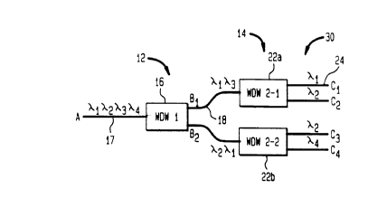
2s Fig. 2 illustrates a first ernbodirnent 30 of the generalized cornb splitting system
10 of Fig. 1 and is meant to be a nonlirniting example, and Fig. 3 gldp~ - ily illustrates the
passbands associated with the first and second stage WDMs 16, 22 of Fig. 1. As shown
in Fig. 1, the cornb splitting system 30 is a lx4 device, having a lx2 WDM 12 in its first
stage 12 and two lx2 WDMs 22a, 22b in its second stage 14.
217g~3
lo
The first stage WDM 16 commllniratçs with an optical signal on optical path 17
having four channels ~ 2, ~3, ~, which are preferably equally spaced in frequency as
shown at reference numeral 31 in Fig. 3 with the spacing ~ of, for example but not lirnited
to, ~=400 gigahertz (GHz). The first stage WDM 16 has channel spacing equal to ~ and
a periodicity (i.e., the free spectral range, FSR) M~, where M=2 is the first stage split
ratio. Thus, in the demultiplexing rnode, the first stage WDM 16 divides the four
channels into two combs, with ~1~3 in one output and ~2~ in the other, as is further
illustrated in Fig. 3 at reference numeral 32.
The second stage WDMs 22a, 22b have a channel spacing M~ and FSR MN~,
o where N=2 is the second stage split ratio. The tr~n~ cion spectrum of second stage
WDM 22b is shifted by ~ relative to that of second stage WDM 22a, so that the centers
of passbands of both WDMs 22 always line up with the input channels ~I through ~, as
illustrated at reference numerals 33, 34 in Fig. 3. The second stage WDMs 22 thus
further split the cornbs from the first stage WDM 16 into separate channels.
Second Embodiment of the Comb SPliffln~ S~stem
A second ernbodirnent of the cornb splitting system 10 of Fig. 1 is illustrated in
Fig. 4 and generally denoted by reference numeral 40. The comb splitting system 40 is a
lx32 device for c~emllllirlexing a mllhirh~nn~.l signal into 32 WDM channels and 32 PS
signals. In structure, the cornb splitting system 40 has a first stage 12 with a single lx8
combined WDM/PS ll~;l~islll 16 interconnected with a second stage 14 having eight
lx8 WDM/PS ll~chan~ s 22. In çc~nne, each of the cornbined WDM/PS ml~h~nicmc
16, 22 serves as both a WDM and a PS, depending upon the wavelength of a channel.
For purposes of ~lic~ucci~)n, hereafter, a "coarse WDM" (or "CWDM") is a
WDM having a wider b~n~lr~cc and larger FSR than another WDM (i.e., "dense WDM"),
2s and a "dense WDM" (or "DWDM") is a WDM having a narrower b~n-lp~cs and srnaller
FSR than another WDM (i.e., "coarse WDM"). Moreover, the coarse WDM (or
CWDM) is used to separate or combine the PS band and the WDM band.
It is advantageous to include a PS with a WDM for at least the following reasons.
First, some distribution schemes, e.g., bro~lc~cting cable television (TV) signals using
high powered linearized optical fiber amplifiers (LOFA) requires power splitters. Second,
it would be more economically viable to initially employ PSs in inexpensive low speed
non-wavelength-selective tran.cmitters and receivers when the bandwidth requirement is
small, and upgrade the system to a fully WDM network when the bandwidth requirement
becomes large. A suitable WDM/PS mechanism 16, 22 is described in U.S. Patent No.
5,285,305 to Cohen et al.
The comb splitting system 40 is used as a demultiplexer as follows. A coarse
WDM (not shown) combines a PS signal and the WDM channels at the central office and
forwards the combined optical signal to the first stage WDM/PS mechanism 16 via
optical path 17, as shown in Fig. 4. Preferably, the first stage WDM/PS mechanicm 16 is
0 housed in the first remote node (RNl) located near the center of a service area of
typically up to about 480 LUs. Each RNl serves up to 480 LUs, and therefore, there are
typically fifteen WDM/PS mechanismc 16 in a single RNl enclosure, with a single-sheath
(bundle) multi-fiber cable running from the CO to RN1. Each of the eight RN1 outputs
serves a separate pedestal (RN2), which host a second stage WDM/PS mechanism 22
serving four LUs.
Fig. 5 illustrates further details of the preferred ernbodiment of the WDM/PS
mechanism 16 (Fig. 4). With reference to Fig. 5, the WDM/PS mPch~ni~m 16 has a
CWDM 42 at its input. The CWDM 42 splits the two wavelength bands and feeds theminto a lx4 DWDM 44 and a lx4 PS 46, respectively. Each output of the DWDM 44 is
subsequently cornbined with an output of the PS 46, using another CWDM 48 that has
the same spectral response as the CWDM 42. Thus, for one wavelength band (referred
to as the WDM band), the WDM/PS mechanism 16 functions as a WDM, and for the
other wavelength band (the PS band), the WDM/PS mechanism 16 functions
llal~a ~ ly as a PS. If both wavelength bands are present at the input optical path 17,
2s each output optical path 24 gets 1/8 of the power of the PS band and a wavelength
channel of the WDM band.
Extra ports 52 can be added for diagnostic purposes. For example, a 2xS
DWDM and a 2x5 PS can be used instead of lx4's, with the extra output having a
fraction (e.g. 1/10) of the power of the regular outputs, thus providing direct local access
to the PS and WDM signals.
2~79$3~
-- 12
Fig. 6 illustrates further details of the preferred ernbodirnent of the WDM/PS
mechanism 22 (Fig. 4). Each WDM/PS mechanism 22 comprises a CWDM 54
interconnected with a DWDM 56 via optical path 55 and a PS 58 via optical path 57.
The DWDM 56 receives a collection of four WDM signals on optical path 55 and filters
s and separates these channels to provide a restrictive channel on each optical path 24.
Furtherrnore, the PS 58 receives a collection of four broadcast signals on optical path 57
and filters and separates the broadcast signals to provide a Ic~ e broadcast signal on
each of four optical paths 24.
In some cases, e.g., in an optical network unit (ONU) where the WDM/PS
o rnechanism 22 of Fig. 6 are fed to separate detectors for the PS and WDM bands, the
CWDMs 42 (Fig. 5) are not needed.
An example of an allocation plan for the thirty-two WDM channels operated
upon by the cornb splitting system 40 is shown at lcfclc.~e numeral 61 in Fig. 7. Also
shown in Fig. 7 at respective reference numerals 62, 63 are the ideal DWDM passbands
of the first stage WDM/PS mechal~.ls 16 and of one of the second stage WDM/PS
rnechanisms 22. The WDM band is preferably around 1.5 ~lm and the PS band is
preferably around 1.3 ~lm, but they can also be interchanged, or at other wavelengths.
The channel spacing is about 400 GHz (wavelength of about 3.2 nrn). The first stage
WDM/PS m~h~nicm 16 (Fig. 4) has a p~c~n-l spacing of about 400 GHz and FSR of
about 8x400 GHz, and needs no birefringence correction and only a small degree of
p~ccb~n-l fl~tening The second stage DWDMs 56 (Fig. 6) have a passband spacing of
about 8x400 GHz and FSR 32x400 GHz, and do not need p~ccb~n-l flattening and
feedback control. Because of the large passband spacing and small number of splits for
the second stage DWDM 56, a Fourier transforrn based waveguide filter (FF) is
preferably used, instead of a WGR.
The 32 channels occupy a total bandwidth of approximately one hundred nm
from 1.48 ~lm to 1.58 ~m. The wavellongthc outside this wavelength range, namely from
1.43 ~m to 1.88 ~m and from 1.58 ~Lm to 1.63 ~lm, can optionally be used to deliver one
rnore channel to each LU or used for testing purposes. If two channels are delivered to
each LU, a simple CWDM~ e.g., a well known MachZehnder interferorneter, can be used
S,,,,17~84~
in each ONU to separate the two channels. If the extra channels are used for testing, the
FSR of the second stage DWDMs 56 (Fig. 6) can be increased to about 64x400 GHz,
thereby blocking the testing signal from reaching the ONU.
The comb splitting system 40 (Fig. 4) cignifi~ntly ~lim;nich~c crosstalk betweenchannels. In this regard, Fig. 8 shows at reference numeral 71 the power spectrum at the
input of the first stage WDM/PS mechanism 16 when all of the thirty-two channels and
one test channel are active but uncorrelated, with the same power leveLc. Fig. 8 further
shows the spectrum of the first and second stage outputs 18, 24 (Fig. 4) at reference
numerals 72, 73, respectively. Moreover, in Fig. 8, the broken line region 65 represents
o the ideal passband of the first stage WDM/PS mechanism 16 (Fig. 4), and the broken line
region 66 represents the ideal passband of the second stage WDM/PS mechanicm 22
(Fig. 4).
When two stages of WDMs, with crosstalk levels of ~ and ~2. respectively, are
c~cc~ded in the cornb splitting system 40, the crosstalk signal from the first stage (of
relative m~gnitude o,) is reduced by a factor ~2 in the second stage, except for channels
;~dj~çent to the pass channels. The channels at the edges of the passband of the second
stage WDM have a crosstalk reduction of ~ 0.5. Thus, in the final output that passes
channel 9, the crosstalk signals are ch~nn~ic 8 and 10 of relative m~gnitude ~,, channels 7
and 11 of relative m~gnitucle ~,/2, channels 1, 17, 25, and the test channel of relative
m~gnit~lde o~, and ch~nn~lc 2-6, 12- 16, 18-24, and 26-32 of relative m~gnit~de ~,~2. The
accllmlll~ted crosstalk is therefore 3~l+4~2+24~,~2. Realistic crosstalk levels achievable
with our current waveguide technology are o,~0.005 and ~2~0.0025 (ie. -23 and -26 db),
and the accumlll~ted crosstalk is ~0.025 or -16 dB. Note that if a single stage lx32
WDM were used, the accllmlll~ted crosstalk level would be 31~1~0.15 (-7.5 dB), and
2s therefore the mllltict~ge cornb splitting scherne offers an effective crosstalk reduction,
which is an important factor that makes it practical. If sixty-four ch~nn~lc are active, an
a~cumlll~t~d crosstalk would degrade by three dB, but it is still below the required
crosstalk level for digital video ~ "-:ccir~n.
It will be obvious to those skilled in the art that many modifications and variations
rnay be rnade to the ernbodiments as described without s~lb~ ly departing from the
~3 1 79843
spirit and scope of the present invention. It is inten-ltod that all such rnodifications and
variations be included herein within the scope of the present invention, as is set forth in
the appended claims.