Language selection

Search

Patent 2180172 Summary

Third-party information liability

Some of the information on this Web page has been provided by external sources. The Government of Canada is not responsible for the accuracy, reliability or currency of the information supplied by external sources. Users wishing to rely upon this information should consult directly with the source of the information. Content provided by external sources is not subject to official languages, privacy and accessibility requirements.

Claims and Abstract availability

Any discrepancies in the text and image of the Claims and Abstract are due to differing posting times. Text of the Claims and Abstract are posted:

  • At the time the application is open to public inspection;
  • At the time of issue of the patent (grant).
(12) Patent: (11) CA 2180172
(54) English Title: ARRANGEMENT FOR MATCHING AND TUNING A SURFACE ACOUSTIC WAVE FILTER
(54) French Title: DISPOSITIF POUR ACCORDER UN FILTRE A ONDES ACOUSTIQUES DE SURFACE
Status: Expired
Bibliographic Data
(51) International Patent Classification (IPC):
  • H03H 9/48 (2006.01)
  • H03H 7/42 (2006.01)
  • H03H 9/145 (2006.01)
  • H03H 9/64 (2006.01)
(72) Inventors :
  • BARDAL, SIGMUND (Norway)
(73) Owners :
  • NORSPACE AS (Norway)
(71) Applicants :
  • AME SPACE AS (Norway)
(74) Agent: ROBIC
(74) Associate agent:
(45) Issued: 2004-01-20
(22) Filed Date: 1996-06-27
(41) Open to Public Inspection: 1996-12-29
Examination requested: 1999-07-13
Availability of licence: N/A
(25) Language of filing: English

Patent Cooperation Treaty (PCT): No

(30) Application Priority Data:
Application No. Country/Territory Date
952589 Norway 1995-06-28

Abstracts

English Abstract

The present invention relates to an arrangement for matching and tuning the impedance of a high frequency surface acoustic wave (SAW) filter (3) to the characteristic impedance of an external system. The arrangement include a power divider/combiner (9,10) with 180 degrees phase difference between the two output ports of the divider - or input ports of the combiner - and adjustable capacitor means (15,24) installed between the power divider/combiner (9,10) and the SAW-filter (3). The arrangement may be a microstrip network where the powerdivider/combiner includes a Wilkinson-divider (9,10) in combination with a 180 degrees phase-shift (11,12) between the output arms (13,14;20,21) of the divider (9,10)


French Abstract

La présente invention concerne un agencement pour apparier et syntoniser l'impédance d'un filtre (3) d'onde acoustique de surface (SAW) haute fréquence avec l'impédance caractéristique d'un système externe. L'agencement inclut un répartiteur/combinateur de puissance (9, 10) avec une différence de phase de 180 degrés entre les deux ports de sortie du répartiteur ou les ports d'entrée du combinateur et un moyen de condensateur ajustable (15, 24) installé entre le répartiteur/combinateur de puissance (9, 10) et le filtre de SAW (3). L'agencement peut être un réseau en microruban où le répartiteur/combinateur de puissance inclut un répartiteur Wilkinson (9, 10) en combinaison avec un décalage de phase à 180 degrés (11, 12) entre les bras de sortie (13, 14 ; 20, 21) du répartiteur (9, 10).

Claims

Note: Claims are shown in the official language in which they were submitted.


6
WHAT IS CLAIMED IS:
1. Arrangement including a power divider/
combiner with 180 degrees phase difference between two
output ports of a divider - or input ports of a combiner,
characterized in that said arrangement includes capacitor
means (15,24) connected between the power divider/combiner
(9,10) and a surface acoustic wave (SAW) filter (3), for
matching and tuning the impedance of the SAW filter (3) to
the characteristic impedance of an external system, the
capacitor means being connected to the SAW filter via
conductive paths having their length adjustable between
said SAW filter and said capacitor means.
2. Arrangement according to claim 1, charac-
terized in that the arrangement is a microstrip network
where the power divider/combiner includes a Wilkinson-
divider (9,10) in combination with a 180 degrees phase-
shifter (11, 12) between the output arms (13,14;20,21) of
the divider (9,10).
3. Arrangement according to claim 1, charac-
terized in that the capacitor means is constituted by a
capacitor (15) connected between two parallell microstrip
lines (13,14), and that said tuning is achieved by
adjusting the lateral position of the capacitor between the
microstrip lines before fixing it in the correct position.
4. Arrangement according to claim 2, charac-
terized in that the capacitor means is constituted by a
capacitor (5) connected between two parallel microstrip
lines (13, 14), and that said tuning is achieved by


7


adjusting the lateral position of the capacitor between the
microstrip lines before fixing it in the correct position.
5. Arrangement according to claim 1, charac-
terized in that that the capacitor means is constituted by
a capacitor with fixed position (24), and said conductive
paths are constituted of two parallell microstrip lines
(20,22,21,23) having adjustable length.
6. Arrangement according to claim 2, charac-
terized in that the capacitor means is constituted by a
capacitor with fixed position (24), and said conductive
paths are constituted of two parallel microstrip lines (20,
22,21,23) having adjustable length.
7. Arrangement according to claim 5, charac-
terized in that adjustablility of the length of the
microstrip lines (20,22,21,23) is obtained by manipulating
a number of bond wires (29) used to bridge gaps (25-28) in
the lines.
8. Arrangement according to claim 6, charac-
terized in that adjustability of the length of the
microstrip lines (20,22,21,23) is obtained by manipulating
a number of bond wires (29) used to bridge gaps (25-28) in
the lines.
9. Arrangement according to claim 7, charac-
terized in that with the microstrip lines (22,23) are 50
ohms lines with one gap in each line, each gap being
bridged by at least two bond wires (29), the bond wires
being 1-3 mm long with a diameter of 0.01-0.1 mm.


8


10. Arrangement according to claim 8, charac-
terized in that the microstrip lines (22,23) are 50 ohms
lines with one gap in each line, each gap being bridged by
at least two bond wires (29), the bond wires being 1-3 mm
long with a diameter of 0.01-0.2 mm.

Description

Note: Descriptions are shown in the official language in which they were submitted.


CA 02180172 2003-O1-23
1
ARRANGEMENT FOR MATCHING AND TURNING A
SURFACE ACOUSTIC WAVE FILTER
The present invention relates to an arrangement
for matching and tuning a Surface Acoustic Wave filter
(SAW-filter) to the characteristic impedance ZO of an
external system, in order to redu~Je reflection losses.
Typically ZO=50 ohms . 'rhe SAW--f i1 ters normally have a high
impedance (capacitive). The arrangement includes a power
divider/combiner with 180 degrees phase difference between
the two output ports of t:he divider - or ink-gut ports of the
combiner.
The insertion-loss of the filter is very
sensitive to loss in the matching network clue to its high
Q-value. Additional requirements are simplicity in tuning
and manufacturability. Tuning of the matching network is
required due to manufacturing variations in the SAW filter
impedance.
At lower frequencies (< 500 MHz) T,rarious
L or
Pi


networks are used, - consisting of ~~apaci=ors, inductors


and possibly resistors. The main principle ,~f prior art
the


arrangements is to compensate for the SAW-filter


capacitance by either a shun'': or a seri es inductor, and


normally with ~f the resulting
an additional
transformation


real impedance e~_~anceZ0. Tuning
into the <:haracteristic
imp


is normally accomplished by adjusting the windings of one
or more inductors.
Solutions utilizing inductors become lossy higher
frequencies ( >500 MHz) . This is true pantic:ularly when
using high-permeak~=i.~ity materials whicr, normally is
required in order to confine the magnetic fields such that

CA 02180172 2003-O1-23
7
direct magnetic coupling between input and output of the
filler is minimized (RE~-isolation). In addition,
- parasitic_ effer_ts are relatively difficult to predict
with high accuracy. T:~ier_e is also a model Li.ng difficulty
related to the definit-i_on of a ground-plane of the matching
network.
The object of the present invention is to provide
a matching system fc;r SAW-filters, particularly in the
high-frequency range above 500 MHz. This is obtained with
the arrangement defined in the claims.
The basic idea is to avoid inductors by
transforming the SAW-filter impedance, and vompensating the
transformed impedance with a .hunt capacitor. The solution
is realized with no via-holes and ground-connec~tions from
the substrate or PCB.
According to the present inven:~ion, there is
provided an arrangement ~nciuding a power divider/ combiner
caith 180 degrees phase differ_Ence between two output ports
of a divider - or input ports of a combinez, characterized
in that said arrangement includes capacitor means (15,29)
connected between the power divider/combiner (9,i0) and a
surface acoustic waU_f ( SAW) f i1 ter ; ~ ) , f~~r matching and
tuning the impedance of the SAW filteo (3) to the
characteristic impedance of an external system, the
capacitor means being connected to the >;AW filter vi.a
conductive paths having their ~.engtr~ adjuistac~ie between
said SAW filter and sal:i capacitor means.
The capacitor means is not itself adjustable.
Preferably, in one embodiment 1 the position of the
capacitor is adjusted to different positions, -in a further
embodiment the capacitor has a fixed position but bound

CA 02180172 2003-O1-23
2a
wires are adjusted to simulate different mounting positions
of the capacitor.
In a pr~aferred embodiment the object of the
invention is achie~~-ed by a microstrip unbalanced to
balanced conversion based on a standard Wilkir.son-divider
in combination v~ith a 180 decrees phase-shift between the
two output arms of the divider.
It is well known in the prior art - such as e.g.
US Patent No 4, 8 70, '76 - to use Wilkinsoo: cornbiners and
i0 microstrip line arrangements in connection with SAW
components. Said US patent does, however, relates to
monolithic elastic convolver output circuits, and does not
apply to matching and tuning of SAW-filter t=ransducers.
~JS Patent No 4, 46C', 877 relates ro a broad-band
printed-circuit balun employing coupled-:->trip all pass
filters. One embodiment of the described ~vaalun (balanced/
unbalanced device) emplcys a Wi'~kinson power
divider/combiner.
The following advantages are obtained with the
20 present invention:
- Matching of high-frequency SAW-filters minimizing
excess losses.
- Simple manufacturing and tuning.
- No inductors and grcmnd-connectiorus (only the
substrate/PCB groundplane, no ~:.-ias; , ensures straight-
forward and accurate simulation and realization.
- Due to the r,alar:wec.~ nature of the SAW filter feedLng,
the problem with direct electromagnetic c~~upling between


3 2180172
input and output is minimized,
Above mentioned and other features and objects of the
present invention will clearly appear from the following
detailed description of embodiments of the invention taken in
conjunction with the drawings, where
Figure 1 illustrates a first embodiment of the invention
and
Figure 2 illustrates a second embodiment of the invention,
In Figure 1 - which is not drawn to scale - items 1 and 2
are input and output matching networks whereas item 3 is a
SAW-filter consisting of interdigital transducers 4 and 5,
arranged on a piezoelectric crystal 6. Interconnections from
items 1 and 2 to item 3 are not illustrated. The input and
output matching networks are identical except for the
interchange of input and output ports, 1.e. the output
network 2 is a mirrored version of the input network 1. Hence
a description is only given of the input network 1.
The input matching network consists of a substrate 7 of
ceramic or PCs materials. A metal pattern forms microstrip
lines with characteristic impedances described below. The
variation in thickness of the various drawn lines indicates
difference in impedance. The input microstrip 8 is of the same
characteristic impedance ZO as the output impedance of
external circuitry. A Wilkinson-divider 9 consists of two
microstrip arms with characteristic impedance ~ 20, each of
the arms with a physical length corresponding to a 90 degrees
phase shift, and a resistor 10, - R=2Z0. At the output of the
Wilkinson-divider there is a 180 degrees phase-shifter. This
consists of two microstrip lines 11 and 12, with
characteristic impedance Z0, and with a difference in physical
length corresponding to a 180 degrees phase-shift.
The function of the Wilkinson-divider is a conversion from
unbalanced to balanced feeding of the SAW-filter. This can be
achieved with any power-divider with a 180 degrees ghase
shift. Two microstrip lines 13 and 14 of characteristic
impedance Z0, are the first part of the lines connecting th.e
phase-shifter to the SAW filter. These two lines are parallel
and has a separation corresponding to the.length of the


- - 4 2180172
' ~ apacitor 15, which connects these lines. The length of lines
13 and 14 is the range where the capacitor can be positioned.
The length of the remaining part of the microatrip line
connecting the phase-shifter to the SAW filter, 16 and 17, is
given by the SAW-filter impedance, the characteristic
impedance and the operating frequency of the SAW filter. These
lines which are shown as straight lines, can be given an
arbitrary path as long as they have the same length.
Tuning of_the matching network ie performed by adjusting
the position of the capacitor along the two lines 13 and 19:,
before fixing it in the correct position.
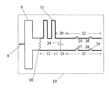
In Figure 2 a matching network 19 illustrates a second
embodiment of the invention. The reference numbers 8-12 shows
components which are identical with components described in
connection with Figure 1. Leading from lines 11 and 12 are
microstrip lines 20/22 and 21/23 as indicated. These llnea
which are shown as straight lines 1n Figure 2, can be given an
arbitrary path as long as they have the same length. A fixed
capaeltor 24 is positioned between lines'20 and 21. A number
of gaps 25-28 are arranged in the lines 22 and 23. Each of
the gaps is bridged with a number (2-5) of bond wires 29.
Tuning of the matching network is done by cutting one or mare
of the bond wires 29 of one or more of the bridged gaps 25-28.
This corresponds to changing the effective electrical length
of the lines 21 and 23, and therefore performs the same
function as moving the capacitor as described in connection
with Figure 1.
Consider an example where the line segments (22,23) are 50
ohms, with one gap in each segment, and wlCh each gap being
bridged by two bond-wires. if the band-wires are 2 mm long and
with a diameter of 0.025 mm, cutting one of the bond-wires in
each gap, gives an increased electrical length corresponding
to a lateral shift of the capacitor by 0.2 mm. The bond wires
could be 1-3 mm long with a diameter of 0.01-0.1 mm.
The above mentioned embodimante of this invention must be
taken as examples only and should not be considered as
limitations on the scope of protection. For example, - the
characteristic impedance of the microstrip lines


- 5 2180172
(11,12,13,19,16,17) can have a different value than zp, - say
z1, - as long as the characteristic impedance of the arms of
the Wilkinaon-divider 9 is changed accordingly, - so that Zl
is transformed into zp at the Wilkinson-divider input 8,

Representative Drawing
A single figure which represents the drawing illustrating the invention.
Administrative Status

For a clearer understanding of the status of the application/patent presented on this page, the site Disclaimer , as well as the definitions for Patent , Administrative Status , Maintenance Fee  and Payment History  should be consulted.

Administrative Status

Title Date
Forecasted Issue Date 2004-01-20
(22) Filed 1996-06-27
(41) Open to Public Inspection 1996-12-29
Examination Requested 1999-07-13
(45) Issued 2004-01-20
Expired 2016-06-27

Abandonment History

There is no abandonment history.

Payment History

Fee Type Anniversary Year Due Date Amount Paid Paid Date
Application Fee $0.00 1996-06-27
Registration of a document - section 124 $0.00 1997-01-16
Maintenance Fee - Application - New Act 2 1998-06-29 $100.00 1998-05-25
Maintenance Fee - Application - New Act 3 1999-06-28 $100.00 1999-05-20
Request for Examination $400.00 1999-07-13
Maintenance Fee - Application - New Act 4 2000-06-27 $100.00 2000-05-17
Maintenance Fee - Application - New Act 5 2001-06-27 $150.00 2001-06-01
Maintenance Fee - Application - New Act 6 2002-06-27 $150.00 2002-05-29
Maintenance Fee - Application - New Act 7 2003-06-27 $150.00 2003-05-30
Final Fee $300.00 2003-10-31
Maintenance Fee - Patent - New Act 8 2004-06-28 $200.00 2004-05-13
Registration of a document - section 124 $100.00 2005-03-18
Registration of a document - section 124 $100.00 2005-04-15
Maintenance Fee - Patent - New Act 9 2005-06-27 $200.00 2005-05-27
Maintenance Fee - Patent - New Act 10 2006-06-27 $250.00 2006-05-24
Maintenance Fee - Patent - New Act 11 2007-06-27 $250.00 2007-05-28
Maintenance Fee - Patent - New Act 12 2008-06-27 $250.00 2008-05-23
Maintenance Fee - Patent - New Act 13 2009-06-29 $250.00 2009-06-11
Maintenance Fee - Patent - New Act 14 2010-06-28 $250.00 2010-06-10
Maintenance Fee - Patent - New Act 15 2011-06-27 $450.00 2011-06-16
Maintenance Fee - Patent - New Act 16 2012-06-27 $450.00 2012-06-15
Maintenance Fee - Patent - New Act 17 2013-06-27 $450.00 2013-06-17
Maintenance Fee - Patent - New Act 18 2014-06-27 $450.00 2014-06-16
Maintenance Fee - Patent - New Act 19 2015-06-29 $450.00 2015-06-15
Owners on Record

Note: Records showing the ownership history in alphabetical order.

Current Owners on Record
NORSPACE AS
Past Owners on Record
ALCATEL SPACE NORWAY AS
AME SPACE AS
BARDAL, SIGMUND
Past Owners that do not appear in the "Owners on Record" listing will appear in other documentation within the application.
Documents

To view selected files, please enter reCAPTCHA code :


To view images, click a link in the Document Description column. To download the documents, select one or more checkboxes in the first column and then click the "Download Selected in PDF format (Zip Archive)" or the "Download Selected as Single PDF" button.

List of published and non-published patent-specific documents on the CPD .

If you have any difficulty accessing content, you can call the Client Service Centre at 1-866-997-1936 or send them an e-mail at CIPO Client Service Centre.


Document
Description 
Date
(yyyy-mm-dd) 
Number of pages   Size of Image (KB) 
Cover Page 2003-12-17 1 35
Representative Drawing 1998-08-19 1 10
Representative Drawing 2002-09-11 1 5
Description 2003-01-23 6 206
Claims 2003-01-23 3 82
Cover Page 1996-10-08 1 11
Abstract 1996-10-08 1 14
Description 1996-10-08 5 164
Claims 1996-10-08 2 52
Drawings 1996-10-08 2 16
Abstract 2004-01-19 1 14
Drawings 2004-01-19 2 16
Description 2004-01-19 6 206
Assignment 1996-06-27 8 232
Prosecution-Amendment 1999-07-13 1 33
Prosecution-Amendment 2002-10-07 2 64
Prosecution-Amendment 2003-01-23 9 278
Correspondence 2003-10-31 1 26
Assignment 2005-03-18 9 270
Assignment 2005-04-15 4 117
Correspondence 2010-08-10 1 46