Some of the information on this Web page has been provided by external sources. The Government of Canada is not responsible for the accuracy, reliability or currency of the information supplied by external sources. Users wishing to rely upon this information should consult directly with the source of the information. Content provided by external sources is not subject to official languages, privacy and accessibility requirements.
Any discrepancies in the text and image of the Claims and Abstract are due to differing posting times. Text of the Claims and Abstract are posted:
| (12) Patent: | (11) CA 2180400 |
|---|---|
| (54) English Title: | PAPER BUFFERING MATERIAL FOR PRE-PACKING ELECTRONIC PRODUCTS |
| (54) French Title: | MATERIAU ANTICHOC A BASE DE PAPIER POUR LE PREEMBALLAGE DE PRODUITS ELECTRONIQUES |
| Status: | Expired and beyond the Period of Reversal |
| (51) International Patent Classification (IPC): |
|
|---|---|
| (72) Inventors : |
|
| (73) Owners : |
|
| (71) Applicants : |
|
| (74) Agent: | AVENTUM IP LAW LLP |
| (74) Associate agent: | |
| (45) Issued: | 2000-02-22 |
| (22) Filed Date: | 1996-07-03 |
| (41) Open to Public Inspection: | 1997-02-01 |
| Examination requested: | 1996-07-03 |
| Availability of licence: | N/A |
| Dedicated to the Public: | N/A |
| (25) Language of filing: | English |
| Patent Cooperation Treaty (PCT): | No |
|---|
| (30) Application Priority Data: | ||||||
|---|---|---|---|---|---|---|
|
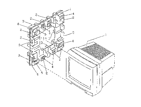
A paper buffering material for pre-packing an electronic
product which can replace the conventional foamed polystyrene
resin. The buffering material includes a paper panel of
predetermined width and shape, which has a plurality of grooves in
predetermined portions thereof to fix and support the electronic
product and a plurality of ribs on both surfaces of the panel to
buffer external impacts.
Note: Claims are shown in the official language in which they were submitted.
Note: Descriptions are shown in the official language in which they were submitted.
2024-08-01:As part of the Next Generation Patents (NGP) transition, the Canadian Patents Database (CPD) now contains a more detailed Event History, which replicates the Event Log of our new back-office solution.
Please note that "Inactive:" events refers to events no longer in use in our new back-office solution.
For a clearer understanding of the status of the application/patent presented on this page, the site Disclaimer , as well as the definitions for Patent , Event History , Maintenance Fee and Payment History should be consulted.
| Description | Date |
|---|---|
| Inactive: Adhoc Request Documented | 2018-06-06 |
| Appointment of Agent Requirements Determined Compliant | 2018-05-18 |
| Revocation of Agent Requirements Determined Compliant | 2018-05-18 |
| Time Limit for Reversal Expired | 2010-07-05 |
| Letter Sent | 2009-07-03 |
| Grant by Issuance | 2000-02-22 |
| Inactive: Cover page published | 2000-02-21 |
| Amendment After Allowance Requirements Determined Compliant | 1999-12-10 |
| Letter Sent | 1999-12-10 |
| Inactive: Amendment after Allowance Fee Processed | 1999-11-22 |
| Amendment After Allowance (AAA) Received | 1999-11-22 |
| Inactive: Final fee received | 1999-11-22 |
| Pre-grant | 1999-11-22 |
| Notice of Allowance is Issued | 1999-05-26 |
| Letter Sent | 1999-05-26 |
| Notice of Allowance is Issued | 1999-05-26 |
| Inactive: Status info is complete as of Log entry date | 1999-05-20 |
| Inactive: Application prosecuted on TS as of Log entry date | 1999-05-20 |
| Inactive: Approved for allowance (AFA) | 1999-05-11 |
| Application Published (Open to Public Inspection) | 1997-02-01 |
| Request for Examination Requirements Determined Compliant | 1996-07-03 |
| All Requirements for Examination Determined Compliant | 1996-07-03 |
There is no abandonment history.
The last payment was received on 1999-05-20
Note : If the full payment has not been received on or before the date indicated, a further fee may be required which may be one of the following
Patent fees are adjusted on the 1st of January every year. The amounts above are the current amounts if received by December 31 of the current year.
Please refer to the CIPO
Patent Fees
web page to see all current fee amounts.
| Fee Type | Anniversary Year | Due Date | Paid Date |
|---|---|---|---|
| MF (application, 2nd anniv.) - standard | 02 | 1998-07-03 | 1998-06-30 |
| MF (application, 3rd anniv.) - standard | 03 | 1999-07-05 | 1999-05-20 |
| Final fee - standard | 1999-11-22 | ||
| 1999-11-22 | |||
| MF (patent, 4th anniv.) - standard | 2000-07-03 | 2000-06-08 | |
| MF (patent, 5th anniv.) - standard | 2001-07-03 | 2001-06-18 | |
| MF (patent, 6th anniv.) - standard | 2002-07-03 | 2002-06-17 | |
| MF (patent, 7th anniv.) - standard | 2003-07-03 | 2003-06-19 | |
| MF (patent, 8th anniv.) - standard | 2004-07-05 | 2004-06-16 | |
| MF (patent, 9th anniv.) - standard | 2005-07-04 | 2005-06-07 | |
| MF (patent, 10th anniv.) - standard | 2006-07-03 | 2006-06-07 | |
| MF (patent, 11th anniv.) - standard | 2007-07-03 | 2007-06-07 | |
| MF (patent, 12th anniv.) - standard | 2008-07-03 | 2008-06-10 |
Note: Records showing the ownership history in alphabetical order.
| Current Owners on Record |
|---|
| LG ELECTRONICS INC. |
| Past Owners on Record |
|---|
| YOUNG HO SON |

