Une partie des informations de ce site Web a été fournie par des sources externes. Le gouvernement du Canada n'assume aucune responsabilité concernant la précision, l'actualité ou la fiabilité des informations fournies par les sources externes. Les utilisateurs qui désirent employer cette information devraient consulter directement la source des informations. Le contenu fourni par les sources externes n'est pas assujetti aux exigences sur les langues officielles, la protection des renseignements personnels et l'accessibilité.
L'apparition de différences dans le texte et l'image des Revendications et de l'Abrégé dépend du moment auquel le document est publié. Les textes des Revendications et de l'Abrégé sont affichés :
| (12) Brevet: | (11) CA 2180400 |
|---|---|
| (54) Titre français: | MATERIAU ANTICHOC A BASE DE PAPIER POUR LE PREEMBALLAGE DE PRODUITS ELECTRONIQUES |
| (54) Titre anglais: | PAPER BUFFERING MATERIAL FOR PRE-PACKING ELECTRONIC PRODUCTS |
| Statut: | Périmé et au-delà du délai pour l’annulation |
| (51) Classification internationale des brevets (CIB): |
|
|---|---|
| (72) Inventeurs : |
|
| (73) Titulaires : |
|
| (71) Demandeurs : |
|
| (74) Agent: | AVENTUM IP LAW LLP |
| (74) Co-agent: | |
| (45) Délivré: | 2000-02-22 |
| (22) Date de dépôt: | 1996-07-03 |
| (41) Mise à la disponibilité du public: | 1997-02-01 |
| Requête d'examen: | 1996-07-03 |
| Licence disponible: | S.O. |
| Cédé au domaine public: | S.O. |
| (25) Langue des documents déposés: | Anglais |
| Traité de coopération en matière de brevets (PCT): | Non |
|---|
| (30) Données de priorité de la demande: | ||||||
|---|---|---|---|---|---|---|
|
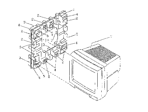
A paper buffering material for pre-packing an electronic
product which can replace the conventional foamed polystyrene
resin. The buffering material includes a paper panel of
predetermined width and shape, which has a plurality of grooves in
predetermined portions thereof to fix and support the electronic
product and a plurality of ribs on both surfaces of the panel to
buffer external impacts.
Note : Les revendications sont présentées dans la langue officielle dans laquelle elles ont été soumises.
Note : Les descriptions sont présentées dans la langue officielle dans laquelle elles ont été soumises.
2024-08-01 : Dans le cadre de la transition vers les Brevets de nouvelle génération (BNG), la base de données sur les brevets canadiens (BDBC) contient désormais un Historique d'événement plus détaillé, qui reproduit le Journal des événements de notre nouvelle solution interne.
Veuillez noter que les événements débutant par « Inactive : » se réfèrent à des événements qui ne sont plus utilisés dans notre nouvelle solution interne.
Pour une meilleure compréhension de l'état de la demande ou brevet qui figure sur cette page, la rubrique Mise en garde , et les descriptions de Brevet , Historique d'événement , Taxes périodiques et Historique des paiements devraient être consultées.
| Description | Date |
|---|---|
| Inactive : Demande ad hoc documentée | 2018-06-06 |
| Exigences relatives à la nomination d'un agent - jugée conforme | 2018-05-18 |
| Exigences relatives à la révocation de la nomination d'un agent - jugée conforme | 2018-05-18 |
| Le délai pour l'annulation est expiré | 2010-07-05 |
| Lettre envoyée | 2009-07-03 |
| Accordé par délivrance | 2000-02-22 |
| Inactive : Page couverture publiée | 2000-02-21 |
| Exigences de modification après acceptation - jugée conforme | 1999-12-10 |
| Lettre envoyée | 1999-12-10 |
| Inactive : Taxe de modif. après accept. traitée | 1999-11-22 |
| Modification après acceptation reçue | 1999-11-22 |
| Inactive : Taxe finale reçue | 1999-11-22 |
| Préoctroi | 1999-11-22 |
| Un avis d'acceptation est envoyé | 1999-05-26 |
| Lettre envoyée | 1999-05-26 |
| Un avis d'acceptation est envoyé | 1999-05-26 |
| Inactive : Renseign. sur l'état - Complets dès date d'ent. journ. | 1999-05-20 |
| Inactive : Dem. traitée sur TS dès date d'ent. journal | 1999-05-20 |
| Inactive : Approuvée aux fins d'acceptation (AFA) | 1999-05-11 |
| Demande publiée (accessible au public) | 1997-02-01 |
| Exigences pour une requête d'examen - jugée conforme | 1996-07-03 |
| Toutes les exigences pour l'examen - jugée conforme | 1996-07-03 |
Il n'y a pas d'historique d'abandonnement
Le dernier paiement a été reçu le 1999-05-20
Avis : Si le paiement en totalité n'a pas été reçu au plus tard à la date indiquée, une taxe supplémentaire peut être imposée, soit une des taxes suivantes :
Les taxes sur les brevets sont ajustées au 1er janvier de chaque année. Les montants ci-dessus sont les montants actuels s'ils sont reçus au plus tard le 31 décembre de l'année en cours.
Veuillez vous référer à la page web des
taxes sur les brevets
de l'OPIC pour voir tous les montants actuels des taxes.
| Type de taxes | Anniversaire | Échéance | Date payée |
|---|---|---|---|
| TM (demande, 2e anniv.) - générale | 02 | 1998-07-03 | 1998-06-30 |
| TM (demande, 3e anniv.) - générale | 03 | 1999-07-05 | 1999-05-20 |
| Taxe finale - générale | 1999-11-22 | ||
| 1999-11-22 | |||
| TM (brevet, 4e anniv.) - générale | 2000-07-03 | 2000-06-08 | |
| TM (brevet, 5e anniv.) - générale | 2001-07-03 | 2001-06-18 | |
| TM (brevet, 6e anniv.) - générale | 2002-07-03 | 2002-06-17 | |
| TM (brevet, 7e anniv.) - générale | 2003-07-03 | 2003-06-19 | |
| TM (brevet, 8e anniv.) - générale | 2004-07-05 | 2004-06-16 | |
| TM (brevet, 9e anniv.) - générale | 2005-07-04 | 2005-06-07 | |
| TM (brevet, 10e anniv.) - générale | 2006-07-03 | 2006-06-07 | |
| TM (brevet, 11e anniv.) - générale | 2007-07-03 | 2007-06-07 | |
| TM (brevet, 12e anniv.) - générale | 2008-07-03 | 2008-06-10 |
Les titulaires actuels et antérieures au dossier sont affichés en ordre alphabétique.
| Titulaires actuels au dossier |
|---|
| LG ELECTRONICS INC. |
| Titulaires antérieures au dossier |
|---|
| YOUNG HO SON |

