Note: Descriptions are shown in the official language in which they were submitted.
WO 95/18961 2 1 8 0 7 3 6 PCT/US94/14603
,~-T ACTIVE ~MPF!R~ nRF! Rr~OR
The present invention generally relates to noncontact
temperature measuring systems, and in particular, devices and
methods for infrared temperature measurement wherein error
inducing signals are isolated and removed to insure reading
5 accuracy.
P~ ~ _ OF ~ r. v ~
To measure temperature by means of infrared emission,
thermal (infrared) radiation may be detected by many sensors
10 known in the art. Thermal radiation has ele- LL ~nPtic
nature and thus can be detected either by quantum detectors
or by thermal detectors. Quantum detectors, such as
photoresistors or photodiodes, require cryogenic cooling to
measure relatively low temperatures with high accuracy. On
15 the other hand, thermal detectors, while not as sensitive as
quantum, may operate at normal room temperatures. This
invention relates to thermal detectors whose most popular
application is in noncontact ther-mometers. One example of
such a thP ter is an instant medical ear th~ ~ter
20 which is capable of noncontact measuring temperatures from
tympanic membrane and surrounding tissues. Thermal sensors
commonly used in infrared thP Lers are thermopiles,
pyroelectrics, bolometers, and active infrared detectors.
The purpose of an infrared sensor is to generate an
25 electrical signal which is representative of net infrared
flux ~ existing between the sensor and the object of
mea~iu- ~ L. The flux depends of two temperatures: the
sensor's own surface temperature Ts and that of the object
(target) Tb. A relation-ship between the two temperatures
30 and the flux is governed by Stefan-Boltzmann law:
~ = k~b~s(Tb4--Ts4) (1)
where b and , are emissivities of the target and sensor
wo 95/18961 2 1 8 0 7 3 6 PCI/US94/14603
respectively, and k is a constant. An ultimate goal of a
temperature meaauL~ L is determination of Tb. It i5 seen
from the above l~quation that to calculate temperature Tb, one
must first determine two variable numbers: a magnitude of
5 infrared flux ~ and the sensor's surface temperature T,.
A surface temperature can be measured by one of many
tem-perature detectors known in the art, like thermistors or
th~' clectrics, while mea~uL~ - ~ of net infrared flux
requires an opto-electronic device known as thermal infrared
10 sensor. There are two classes of thermal infrared sensors:
passive infrared (PIR) and active far infrared tAFIR).
Examples of PIR detectors are pyroelectrics, thermopiles, and
bolometers. Measurement of infrared flux by a PIR sensor is
not a simple task because PIR sensors with a good speed
15 response are g~enerally fabricated in a form of thin flakes
or membranes, whose surface t', at-~L~ T, is not only
difficult to ]~easure, but that temperature changes upon
e~oDuLæ to a target. Inaccurate determination of sensor's
surface temperature T, results in error in a noncontact
20 tempera-ture calculation. Since sensor's surface temperature
in a PIR detector changes upon e~ OauLt: to a target, to
improve response speed of the sensing element, its thermal
capacity must be made very small. This imposes quite
stringent requiremlents to a PIR sensor's design and increases
25 cost.
An AFIR sensor, as opposed to PIR, operates at a pre-
detP-~ni n~l (oEten constant) temperature T~ o~ a sensing
element. The AFIR sensors are based on U. S . Patents Nos .
4,854,730 and S,054,936 issued to Fraden. The operating
30 principle of an AFIR sensor can be illustrated by the
following example. In a sensor's housing, there is a sensing
element which contains a temperature detector (for instance,
a thermistor) and a heater (a constant+resistor). The heater
i6 t-h~ l ly coupled with the detector. The sensing element
35 is connected to an electronic circuit which measures the
element's temperature through a tem-perature detector and
, . . _ . _ . _ _ _ _ _ _ _ _ _ _ _ _
wo 9~/18961 ' ~ 2 1 8 0 7 3 6 PCTiUSg4ll46n3
provides electric current to the heater to elevate its
temperature above ambient. The circuit maintains the
element's temperature on a predet~rminPd T~ level which in
many cases is above the highest temperature of a target.
5 Thus, being warm, an AFIR sensing element becomes a source
of infrared radi-ation whose net flux is guided toward a
target. The magnitude of that flux relates to a temperature
gradient between the known temperature Ts and the unknown
temperature Tb of a target. Under the idealized conditions,
lO according to law of conservation of energy, heat ~ radiated
from the sensor toward the target must be equal to electric
power P supplied to the resistive heater. The idealized
conditions here mean that the only way the element may lose
its thermal energy is by radiating it toward the target.
15 Electric power provided to the heater can be expressed
through value of the heater's resistance, R, and voltage V
acros6 it:
P ~ V2 (2)
20 R
Hence, combining equations (l) and (2), we can calculate
the target temperature as
~\T,4 ~ V2
R~-sgk (3)
It i5 seen that the calculated temperature of a target
depends only of one variable which is the voltage V across
the heating resistor. All other parts of equation (3) are
35 either constant or predetP~m; nPd. Further, if electronic
circuit is efficient in maintaining Ts level inrlPrPn~lPnt of
Tb, the ele-ment's temperature doesn't change upon exposure
to a target and the AFIR sensor becomes not only accurate but
fast as well. This can be accomplished with no stringent
40 requirements to thermal capacity of a sensing element. In
_ _ _ _ _ _ _ , . . _ . . .... . _ . , .... _ _ _ _ _ _ , _
WO95/18961 2 1 80736 PCrNSs~114603
effect, an AFIR sensor is a direct and e~icient converter
of electrical power into thermally radiated power. Value of
Ts typically i5 selected in the range from 40- to l00-C. For
medical applications, i~ is preferably near 50-C.
In reality, an AFIR sensor doesn't operate under
; d~ 11; z~d conditions . Thermal energy dissipated by the
heating resistor, goes not only toward the target, but to all
--ts o~ a sensor's internal structure as well.
Further, heat propagates from the element not only by means
of radiation, but also through thermal conduction and
gravitational convection of gas inside the sensor's housing.
This makes use of formula (3) quite inaccurate, as it doesn't
contain an additional variable whose influence becomes quite
strong. This variable is tempera-ture of the sensor's
lS housing, or, i~- other words, the environ-mental (ambient)
temperature~ That is, a major difficulty in design and use
of AFIR sensors relates to c -n~ating for stray heat loss
from the sensor system.
To ~ -ate for undesirable thermal loss from a
sensing element, several methods and system arrangements have
been proposed. For example, see U.S. Patent No. 4,854,730,
and U.S. Patent No. 5,054,936 issued to the present
~rP~ i c~nt . The tGarh; n~s of these two patents are
incorporated b~y reference as if restated herein in full.
While these approaches have been successful in addressing
some of the error inducing signals associated with AFIR
sensors, there remains a need to enhance overall performance
in signal isolation and reading accuracy. It was with this
understanding of ~he prior art systems that the present
invention was realized.
OBJEC~8 aNn 8~nlMARY OF TliE PRE8~NT lr v~n~lud
It is a goal of the present invention to provide a
method of noncontact temperature measurement where accuracy
of the sensor is substantially i n~ p~n~ nt of ambient
temperature .
WO 95118961 PCTnJSs4/l46o3
It is another object of the present invention to provide
an active infrared temperature sensor with fast response
speed .
It is another object of the present invention to provide
5 an active infrared thP ter which is stable over a broad
operating temperature range.
It is a further object of this present invention to
provide an active infrared sensor having small dimensions.
It is yet a further goal of the present invention to
lO provide an active infrared temperature sensor with
predetP~ninP~ optical properties.
The above and other objects of the present invention are
realized in a specific sensor arrangement wherein two
separate active sensor elements (AFIR) are placed in pre-
15 selected orien-tation within a noncontact thP -ter. By
using two separate and distinct sensor elements, the target
temperature signal can be isolated from other error inducing
signal ~ ~nts normally associated with a single sensor
element. More particularly, the first sensing element is
20 used for emanating far infrared radia-tion toward a target,
while a second, essentially identical sensing element,
isolated from the target, generates a compen-sating signal
reflective of the local environment for both sensing
elements . This latter target i n~lPpPn~Pnt signal is used to
25 ~~ ---ate for local amoient heat transfers, and thus permits
calculation of an accurate target temperature.
To vv~ limitations resulted from thermal crosstalk
between the two separate sensor elements, the sensing
elements are fabricated on separate, thPrr-1 ly decoupled
3 o substrates . Each element has its own electronic control
circuit to maintain its temperature at a known pre-determined
level. Preferably, temperatures of both elements are
substantially the same. Each element contains an auxiliary
heater and control circuit. The control circuit measures
35 element t~ I~L~ and applies heat via the resistor, to
maintain a pre-set element temperature.
_ _ _ _ _, . . . _ _ . . . _ _ . . _ . _ _ _ _ _ _ _ .
wo 9S/18961 ~ 2 1 8 0 7 3 6 PcT/usg4/l46n3
With this arrangement, stray thermal losses from both
elements are nearly equal, while only the radiating element
can emanate thermal radiation toward the target. Since stray
heat loss from the radiating element is ~ ated for by
5 the second element and its control circuit via an auxiliary
heater, the radiating element and its control circuit need
to respond only to the thermally radiated power. Since both
sensing elements are thf-rr-l 1 y insulated from one another,
control circuit~ can operate ; nrlPp~nA~ntly which assures
l0 their stable performance.
.. L~W OF ~H~ FIGURES
Fig. l is a cross-sectional view of an AFIR sensor with
two sensing elenents;
lS Fig. 2 shows a sensing assembly with two sensing
elements supported by a common spacer;
Fig. 3 is an isometric view of a sensor with a
cylindrical opt-ical guide;
Fig. 4 is an iq~ ~-ic view of a sensor with a parabolic
optical guide:
Fig. 5 is an isometric view of a sensor with a conical
optical guide;
Fig. 6 sho~s two AFIR sensing elements held by common
supports;
Fig. 7 is exploded cross-sectional view of an AFIR
sensing element with multiple layers on one surface of a
substrate;
Fig. 8 is exploded cross-sectional view of a sensing
ele-ment with a discrete temperature sensor having axial
3 0 contacts;
Fig. 9 is exploded cross-sectional view of a sensing
ele-ment with a discrete temperature sensor having surface
contacts;
Fig. l0 ic exploded cross-sectional view of a sensing
element with multiple layers on both surfaces of a substrate;
Fig. ll shows a bl--ck diagram of a dual sensor attached
Wo 95/18961 2 1 8 0 7 3 6 PCT/US94/14603
to control circuits; and
Fig. 12 is a sensing assembly with integrated circuit.
rJF~ OF rT~r p~c~ v~ O~
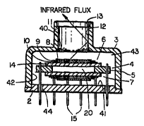
Referring to Fig. l, it is seen that AFIR sensor l is
housed in a protective cap 3 whose purposes are to protect
the interior from contaminations and to equalize thermal
environment for the internal t~,~Lll~ ~ULe Thus, cap 3
preferably should be fabricated of metal, however, some
plastics and ceramics may be used for that purpose as well.
The inner space 43 of sensor l is filled either with dry air
or inert gas. Alternatively, gases may be evacuated to
maintain vacuum in the inner space 43. The upper portion of
cap 3 has an optical opening 40. That opening may be formed
into an optical guide ll to channel infra-red flux toward
desirable direction outside of the sensor. Inner surface 12
of guide ll preferably should be highly reflective. Thus,
it may be polished and gold plated, as gold is the most
effective reflector in the far infrared spectral range.
The outer opening of optical guide 11 is protected by
window 13. The window may be glued or welded to the optical
guide. The window should have good transmitting
characteristics in the far infrared spectral range. While
it can be made of plastics, like polyolefins, the preferred
materials are silicon, germanium, zinc 6elenide, AMTIR or
other suitable hard crystalline or amorphous elements or
compositions. To improve transmitting characteristics, a
window can be given anti-reflecting coatings (ARC) geared for
the operating wavelength.
Cap 3 is attached to header 2 by means of welding,
solder-ing, or by an appropriate binder. Thus the
combination of cap 3, window 13 and header 2 seals inner
space 4 3 .
Inside sensor l, there is a sensing assembly 4 formed
by spacer 5 and two elements 6 and 7. Radiating element 6
faces optical guide, while ~ -ating element 7 faces the
Wo 95/18961 ~ - - 2 1 8 0 7 3 6 PCT/US94114603
surface of header 2. Radiating element 6 i5 optically
coupled to the out-side of the sensor through optical guide
ll and window 13. C ~ncating element is sandwiched between
spacer 5 and header 2. ~urface 41 of header 2 is reflective
and preferably gold plated, thus ~ ting element 7 has
low level of radiation. To further reduce radiative coupling
between elements 6 and 7 and the inner walls of the sensor,
inner surface 42 of cap 3 is also reflective and preferably
gold plated.
Spacer 5 is ring shaped with an opening in the center.
This opening forms an empty cavity ~etween the sensor
Qlements to minimize thermal contact between elements 6 and
7. To further improve thermal insulation, space 20 may be
filled with low thermal conductivity material. Sensing
as6embly 4 i8 ~upported by t~rmi n~l C 15 which also provide
electrical connec-tion to the outside circuits. To assure
tight seal between terminals 15 and header 2, an insulating
eyelets 44 may be used between the surface of terminals 15
and the surface of header 2.
Alternatively, sensing assembly 4 may be designed as
shown in Fig. 6 where elements 6 and 7 are held by several
supports 16 to l9, thus eliminating the need for a separate
spacer 5. In this ~rr~ngf ~, electrical connections to the
terminals may ]~e accomplished through one of several known
techniques, such as wire bonding, conductive epoxy, surface
metallization, etc. As an example, Fig. 6 shows a surface
metallization of support 18. The metallization forms
conductor 22 which is interfaced with element 6 at clamping
area 21. The intended functional properties associated with
the above and other arr~n~ Ls for sensor assembly 4
include mechanical integrity, good thermal insulation between
sensing ele~ents, and electrical connections to sensor
t~n;r~1.
In another embodiment, the sensing elements may be held
inside the AFIR housing by the supports having low
coefficient of thermal conductivity. This will minimize both
_ _ _ _ _ _
Wo 95/18961 2 ~ 8 0 7 3 6 PCT/US94/14603
the thermal crosstalk between the elements and the thermal
10s6 from the elements to the sensor's housing. The
electrical connections between the elements and the t~rmin;~lc
can be accomplished through one of the standard methods known
- 5 in the art, for in-stance, by a wire bonding technique. It
is important for the heat loss reduction to as6ure that the
wire lengths are maxi-mized and the cross-sectional areas are
m; niri 7ed .
For some applications a wide angle of view is required.
In these cases, optical guide may have a cylindrical shape
as it is depicted in Figs. l and 3, where field of view 70-a
is relative-ly wide. In other applications, the optical
guide may be com-pletely omitted. In a sensor without an
optical guide, window 13, may be mounted directly at the rim
of optical opening 40. In some other applications,
especially for fabricating medical thp ters, a narrower
field of view may be required. Then, a focusing lens may be
installed into optical opening 40 instead of a window. Such
a lens must be fabricated of a material with good
transmission characteristics in the far infrared spectral
range .
Alternatively, a nonimaging concentrator may be employed
as an optical guide. Such concentrators are described for
instance in W. T. Welford and R. Wilson, Hiqh Collection
~gn;r^ ~inq ~tir~s. Academic Press Inc., 1989. (The
t~arh;n~e of which are incorporated by reference.) To
illu6trate use of concentrators, Fig. 4 shows optical guide
ll having a parabolic profile and Fig. 5 depicts a guide
having a conical profile. Either optical guide ll is covered
with window 13 and provides a relatively narrow field of view
70-b and 70-c as compared with that shown in Fig. 3. A
parabolic guide is generally more efficient for forming a
narrower field of view than conical, however, the latter is
easier to fabricate.
Returning again to Fig. l, one may observe that each of
identical sensing elements, 6 and 7, is a complex structure.
WO 95/18961 -- 2 1 8 0 7 3 6 PCT/11591/14603
Referring to element 6, this element is ~ ~ -sed of substrate
14 with multilayer depositions on its surface. The order of
layers is not critical, however there should be at least one
tempera-ture sensing layer 8, f irst resistive layer 9, and
5 second resistive layer 10. For the practical purposes of
3~anufactur-ing, it is usually preferable to keep sensing
layer 8 on the top. There can be several electrically
isolating layers be~ween the conductive layers.
A cross-section of an illustrative sensing element
10 (suit-able for either element 6 or 7) is depicted in Fig. 7,
where isolating layers 26 and 27 are shown. In this
arrangement, first and second resistive layers 9 and 10,
respectively, serve as heaters, while sensing layer 8 is for
measuring tempe3-ature of a multilayer structure. The above
15 layers of elem,ent 6 are electrically isolated from one
another and at the same time intimately th~`l Iy coupled to
one another.
Temperature sensing layer 8 may be deposited by
sputtering technique forming a thin film of a semiconducting
20 material which acts as a temperature sensitive resistor. If
a substrate is fabricated of a material with high thermal
conductivity, such as aluminum nitride, a temperature sensing
layer 8 and resistive layers 9 and 10 may be deposited on the
opposite sides 03f sub-strate 14 as it is illustrated in Fig.
25 10. This may simplify sensor fabrication because resistive
layers 9 and 10, and insulating layer 26 may be formed by
using a thick film technology, while temperature sensing
layer 8 is form~d by a thin film technology.
Alternativl~ly, a temperature sensing layer 8 may be re-
30 placed with a discrete temperature sensor. Fig. 8illustrates use of a chip thermistor as temperature sensor
29 positioned on the top of a multilayer assembly.
Temperature se3~sor 29 has end terminations in a form of
conductors 31 which can be soldered or otherwise electrically
35 connected to metal connection 28. Con-ductors 31 may be
position at various sides of temperature sensor 29. Fig. 8
Wo 95/18961 2 1 8 0 7 3 6 PCT/US94/14603
11
shows axial position of conductors 31, while Fig. 9 shows
temperature sensor 29 with top metallization 45 and bottom
metallization 46, which are respectively connected to
connection 28 and conta~t pad 47. Connection 28 and contact
pad 47 provide electrical interface between temperature
sensor 29 and conductors on substrate 14, which,
subsequently, are at-tached to the sensor te~inl1R 15 (not
shown in Figs. 7-10). Discrete temperature sensor 29 must
be well therr~l 1y connected to first and second resistive
layers 9 and 10 to assure fast and efficient thermal control
of the sensing element.
Specific to each arrangement is the requirement that the
very top of the sensing assembly exhibit a high emissivity
in the operating wavelength. Suitably, the upper surface is
formed of metal, like top metallization 45 shown in Fig. 9.
In these cases, the metallic surface must be treated to give
it emissivity ~Yc ee~ i n1 0 . 9 . This can be done by using one
of standard methods known in the art (see, for instance, J.
Fraden. "AIP Handbook of Modern Sensors" , American
Institute of Physics, 1993, page 465, herein incorporated by
ref erence ~ .
By definition, an AFIR sensor is active and, therefore,
requires an external energy source to operate. This function
is accomplished by an electronic circuit. In the present
context of two separate sensor elements, a dual circuit is
required. Fig. 11 illustrates a block diagram of such a
circuit. In this diagram, the bottom section is connected
to ---ating element 7. The circuit consists of a first
error amplifier 32 and first control circuit 34 which has a
3 0 built-in power driver to supply electric current to second
resistive layer 100 of compensating element 7. The circuit
34 also supplies an identical current to second resistive
layer 10 of a radiating element 6. The current is supplied
through conductor 35 and is manifested by output voltage
3 5 Vc~ .
In operation, first error amplifier 32 compares signal
wo 95/18961 2 1 8 ~ 7 3 6 PCr/uss4ll46o3
12
from temperature sensitive layer 80 with first reference
signal V",1 at its reference input 33 and feeds the
difference to first control circuit 34. That circuit
generates output voltage Vcr"4 of such a maqnitude as
nPcec~Ary to maintain the output of temperature sensitive
layer 80 nearly equal to first reference signal Vr,f1. The
reference signal can be produced either by a voltage
reference or by Wheatstone bridge ~not shown). As long as
first reference signal V,~1 is pre-dete~;n~d, temperature of
~ ating element 7 is also maintained on a predQtermined
level, which may or may not be constant, dDpDn~l~ng of a
particular application of the sensor.
Since both elements 6 and 7 are identical and their
resistive layers l0 and l00 are supplied by identical
currents from first control circuit 34, temperatures of these
elements are close to one another. A difference in
temperatures primarily may arise from a difference in optical
conditions of elements 6 and 7. Radiating element 6 is
allowed to emanate infrared flux toward an outsidQ object,
while ~ -ne:~ting element 7 is shielded from that. On the
top, it is prevented from radiating by warm substrate 14
whose temperature is nearly equal to that of substrate 140,
and on the bottom, it faces reflective surface 41 of header
2.
In addition, l:he outer layer of ~ -ating element 7
(which in Fig. ll is temperature sensitive layer 80) may be
metal coated to further reduce its emissivity. Therefore,
-ating sensor may lose heat only through conduction and
convection, while the radiating sensor can do that through
radiation as well. Additional heat loss may result in some
reduction in temperature of radiating element 6. To
---ate fo~- that reduction, signal from temperature
sensing layer 8 is fed into second error amplifier 36 which
has second reference signal Vr,~2 provided to its reference
input 37. Magnitude of Vre,2 is such as to assure equal
temperatures of both sensing elements 6 and 7.
_ _ _ _ _ _ , _
Wo 95118961 2 1 8 0 7 3 6 PCT/US94/14603
Continuing with Fig. 11, error signal from amplifier 36
i5 fed into second control circuit 38 which generates control
signal 39 supplied to first resistive layer 9. Magnitude of
control signal 39 is sufficient to generate heat equal to
radi-ative loss toward a target. That signal is used as an
output voltage Vout~ Since nonradiative loss is nearly
completely c -ncated for by first control circuit 34,
second control circuit 38 needs to ~ CAte only for the
radiative loss from radiating element 6. Hence, output
voltage Vo"t is almost free of influence of ambient
temperature, because ambient temperature detP~minPc
nonradiative loss, while radiative loss is governed by the
temperature of a remote target.
As elements 6 and 7 are separated by space 20 whose
thermal conductivity is very low, both control circuits are
well thPr~l ly decoupled. To make sure that decoupling is
complete, conductor 35 preferably should be thin and long.
Low thermal coupling between sensing elements 6 and 7 assures
stable functioning of the sensor.
In many applications, it may be desirable to incorporate
the sensor temperature control circuits inside the sensor
housing. Most of electronic ~ t:, may be fabricated in
a form of an integrated circuit which can be positioned
directly in the -nC~A~ting element 7 as it is depicted in
Fig . 12 . A general conf iguration of the sensing assembly 4
is substantially the same as described above. The only
dif~erence is that the integrated circuit 72 is bonded on the
surface o~ insulator 71. It is possible to incorporate a
temperature sensing detector inside the integrated circuit
chip, thus, _ ^ating element 7 would not require
t~ c.Lur~ sensing layer 80 as in Fig. 11. Since first
resistive layer 90 generally is not connected to any control
circuit tFig. 11), it can be omitted as in Fig. 12 , where
insulator 71 is deposited on the top of second resistive
layer 100.
The above-described arrangement is merely illustrative
Wo 95/18961 . 2 1 8 0 7 3 6 PCTIIJS94/l46n3
14
of the principles of the present invention. Numerous
~ ;fications and adaptations thereof will be readily
apparent to those skilled in this art without departing from
the spirit and scope of the present invention.