Note: Descriptions are shown in the official language in which they were submitted.
2i80905
DIGITA~ DEMODULATOR
BACKGROUND OF THE INVENTION
Field of the Invention
This invention relates to a digital demodulator for
demodulating received signals for satellite communications,
land-mobile communications, or land-mobile satellite
communications.
Description of the Prior Art
Recently, digital demodulators have been developed in
order to demodulate digitally modulated signals. Such a
digital demodulator demodulates a received signal by
subjecting the signal to analog-to-digital conversion, and
computer-processing a digitized signal.
One such digital demodulator is described in "A New
Coherent Demodulation Technique for Land-Mobile Satellite
Communications" (S. Yoshida, H. Tomita, International Mobile
Satellite Conference, Ottawa, pp 662-627, 1990).
Fig. 6 is a block diagram showing the configuration of
this digital demodulator. The digital demodulator is used to
coherently detect a QPSK-modulated signal. An IF
(intermediate frequency) signal obtained by frequency-
converting a received signal is inputted into the digital
demodulator.
Referring to Fig. 6, an analog-to-digital converter 60
(called the "A/D converter 60") directly samples the input IF
signal at a high sampling rate which is four times the rate of
- ` 21 80905
the IF signal frequency, and digitizes the IF signal. A
digital quadrature detector 62 multiplies a sample signal
(outputted from the A/D converter 60) by two reference -
signals, which have a fixed frequency and phases different
from each other by ~/2, or subjects the sample signal to the
quasi-coherent quadrature detection. The digital quadrature
detector 62 samples-detected results, and generates an output
signal (a detected sample signal) having a bit rate
approximately four times the bit rate of the received signal.
Thus, the detected sample signal is expressed by:
IQC (nT)=I(nT)cos(~nT+~)-Q(nT)sin(~nT+~)
QQC (nT) =Q (nT)cos(~nT+~)+I(nT)sin(~nT+~) ------ (1)
where IQC ( ) and QQC ( ) respectively denote in-phase component
and quadrature components of the detected sample signal; I()
and Q ( ) respectively denote in-phase components and quadrature
components of the original digital signal to be transmitted; _
is an integer; T denotes an interval between two sample times
for the digital quadrature detector 62 to output detected
sample signals; ~ denotes a frequency deviation between a
carrier of the received signal and a frequency of the
reference signal; and ~ denotes an initial phase of the
detected sample signal (i.e. an initial phase of the reference
signal with respect to the received carrier). Further, the
reference signals used for quasi-coherent detection have sine
waves whose frequencies approximate to the frequencies of the
carrier, so that the detected sample signal is a baseband
signal.
2 1 80905
The digital quadrature detector 62 outputs the detected
sample signal, as complex data, to a receiving filter 64. The
receiving filter 64 shapes a waveform of the detected sample
signal, thereby eliminating out-of-band noise components
therefrom.
An output signal from the receiving filter 64 is applied
to a bit timing recovery (BTR) 66, and to an interpolator 68.
The BTR 66 determines bit timing, i.e. decision timing for
deciding a value of the received signal. Information on the
determined decision timing is inputted into the interpolator
68. One example of a method of estimating the decision timing
by the BTR 66 is also described in the foregoing literature
(by Yoshida et al.).
The output signal of the receiving filter 64 is a signal
sampled at oversampling timing, which is not always
synchronous with the decision timing. Therefore, the
interpolator 68 interpolates this output signal, and generates
a decision timing signal expressed by:
IN (mTS) =I (mTs)cos(~mTs+~N)-Q(mTs)sin(~mTs+~N)
20 QN (mTS) =Q (mTS) COS (~mT5+~N) +I (mTs)Sin(~mTS+~N) ------(2)
where IN ( ) and QN ( ) respectively denote in-phase components and
quadrature components of the decision timing signal; Ts
denotes an interval between decision times ti.e. Nyquist
interval)i and ~N denotes an initial phase component of the
decision timing signal.
The interpolator 68 outputs the foregoing decision timing
signal as the complex data at each Nyquist interval. The
21 80905
_
following circuits operate in response to the decision timing
signal. In Fig. 6, a solid line represents a route for
signals which vary at each oversampling interval, while-a
double-solid line represents a route for signals which vary at
the decision timing, i.e. vary at the Nyquist intervals.
In the circuits following the interpolator 68, a phase
rotation component, which is caused by the frequency deviation
(~) and the initial phase (~N), is eliminated from the
decision timing signals IN(mTs) and QN(mTs), thereby recovering
original digital signals I(mTs) and Q (mTS) .
First of all, an automatic frequency controller (AFC) 70
estimates a frequency deviation component, and feeds it back
to a multiplier 72, which eliminates the frequency deviation
component from the decision timing signals IN and QN. Then, a
phase estimator 74 estimates an initial phase ~N on the basis
of the decision timing signal whose frequency deviation
component has been eliminated, and generates a phase
correcting signal on the basis of the initial phase ~N. The
foregoing literature (by Yoshida et al.) describes an example
of the internal configuration of the phase estimator 74. A
multiplier 76 multiplies the decision timing signal (free from
the frequency deviation component) by the phase correcting
signal, thereby eliminating the initial phase component from
the decision timing signal. An output of the multiplier 76
serves as a coherently detected output for the received
slgnal .
In the digital demodulator of Fig. 6, the AFC and the
; 21 80905
phase estimator operate in response to the decision timing
signal. Therefore, when a burst signal or the like is
inputted, neither the AFC nor the phase estimator can operate
until the BTR operates stably. In other words, even when the
AFC and the phase estimator are operated, no correct output is
obtainable before the stable operation of the BTR. In this
state, it is meaningless to operate the AFC and so on. In the
prior art, the AFC is activated after the stable operation of
BTR. The phase estimator is not activated until the AFC
operates stably. Therefore, the digital demodulator of the
prior art is prone to a problem that it cannot satisfy a
request for high speed operation. Further, even when such a
digital demodulator becomes stable, malfunction of the BTR
would lead to erroneous operation of the phase estimator.
Summary of the Invention
The present invention is intended to overcome the
foregoing problems of the prior art, and to provide a digital
demodulator which can operate at a high speed, and is
configured so as to protect circuit components against the
malfunction of the BTR.
According to a first aspect of the invention, there is
provided a digital demodulator for coherently detecting
received digitally-modulated signals, which comprises: a
quasi-coherent detector for quasi-coherently detecting each
received signal on the basis of a predetermined reference
signal and outputting a detected sample signal at each
sampling timing; a decision timing generator for generating
2 1 80905
_
decision timing for the received signal on the basis of the
detected sample signal; an interpolator for interpolating the
detected sample signal on the basis of information concerning
the decision timing, and generating a decision timing signal;
a frequency deviation estimator for estimating a frequency
deviation between a carrier of the received signal and the
reference signal, and generating a frequency deviation
correcting signal in each decision timing on the basis of the
estimated frequency deviation; a frequency deviation corrector
for correcting the decision timing signal, on the basis of the
frequency deviation correcting signal; a phase estimator for
estimating an initial phase component of an output signal of
the frequency deviation corrector and generating a phase
correcting signal on the basis of the initial phase component;
and a phase corrector for correcting the output signal of the
frequency deviation corrector using the phase correcting
signal.
In this arrangement, the frequency deviation estimator
estimates a frequency deviation of the received signal on the
basis of the detected sample signal. The frequency deviation
estimator can estimate the frequency deviation before the
decision timing generator generates the decision timing, i.e.
the frequency deviation is estimated independently of the
decision timing generation. This configuration enables the
digital demodulator to operate at a high speed, and prevents
the frequency deviation estimator from being adversely
affected by the malfunction of the decision timing generator.
21 80905
_
In accordance with a second aspect of the invention, there
is provided a digital demodulator comprising: a quasi-coherent
detector for quasi-coherently detecting each received signal
on the basis of a predetermined reference signal and
outputting a detected sample signal at each sampling timing:
a decision timing generator for generating decision timing for
the received signal on the basis of the detected sample
signali an interpolator for interpolating the detected sample
signal on the basis of information concerning the decision
timing, and generating a decision timing signal; a frequency
deviation estimator for estimating a frequency deviation
between a carrier of the received signal and the reference
signal, and generating a first frequency deviation correcting
signal for each decision timing and a second-frequency
deviation correcting signal for each sampling timing, on the
basis of the estimated frequency deviation; a first frequency
deviation corrector for correcting the decision timing signal
on the basis of the first frequency deviation correcting
signal; a second frequency deviation corrector for correcting
the detected sample signal on the basis of the second
frequency deviation correcting signal; a phase estimator for
estimating an initial phase component of the detected sample
signal on the basis of an output signal of the second
frequency deviation corrector, and generating a first phase
correcting signal for the sampling timing on the basis of the
initial phase component; and a correcting signal modifier for
modifying the first phase correcting signal on the basis of
21 ~05
the decision timing and the first frequency deviation
correcting signal, and generating a second phase correcting
signal for the decision timingi and a phase corrector for
correcting the output signal of the first frequency deviation
corrector on the basis of the second phase correcting signal.
With the digital demodulator, not only the frequency
deviation but also the initial phase component are estimated
on the basis of the detected sample signal. This further
accelerates the operation of the digital demodulator, and
prevents the estimation of the initial phase component from
being adversely affected by the malfunction of the decision
timing generator.
According to a third aspect of the invention, there is
provided a digital demodulator comprising: a quasi-coherent
detector for quasi-coherently detecting each received signal
on the basis of a predetermined reference signal and
outputting a detected sample signal at each sampling timing:
a decision timing generator for generating decision timing for
the received signal on the basis of the detected sample
signal; an interpolator for interpolating the detected sample
signal on the basis of information concerning the decision
timing, and generating a decision timing signal; a delay
detector for delay-detecting the decision timing signal; a
frequency deviation estimator for estimating a frequency
deviation between a carrier of the received signal and the
reference signal on the basis of the detected sample signal,
and generating a phase rotation correcting signal indicative
- - 21 80905
-
of an amount of phase rotation per delay time of the delay
detector, on the basis of the estimated frequency deviation;
and a phase corrector for correcting an output signal of the
delay detector on the basis of the phase rotation correcting
signal.
In this arrangement, the demodulation is performed by
delayed detection. During the demodulation, the frequency
deviation estimator estimates the frequency deviation of the
received signal on the basis of the detected sample signal.
Thus, the frequency deviation estimator can estimate the
frequency deviation before the generation of the decision
timing by the decision timing generator. The frequency
deviation estimation is performed independently of the
generation of the decision timing generation. This enables
the high speed operation of the digital demodulator, and
prevents the frequency deviation estimator from being affected
by the malfunction of the decision timing generator.
The invention will become more apparent from the following
detailed description of the presently preferred embodiments
when taken in conjunction with the accompanying drawings.
Brief Description of the Drawings
Fig. 1 is a block diagram schematically showing the
configuration of a digital demodulator according to a first
embodiment of the invention;
Fig. 2 is a block diagram schematically showing the
configuration of a digital demodulator according to a second
embodiment of the invention;
2 1 80905
Fig. 3 is a block diagram schematically showing the
configuration of a digital demodulator according to a third
embodiment of the invention;
Fig. 4 is a block diagram schematically showing the
configuration of a digital demodulator according to a fourth
embodiment of the invention;
Fig. 5 is a block diagram showing the configuration of a
digital demodulator for performing quasi-coherent qudarature
detection;
Fig. 6 is a block diagram showing the configuration of a
digital demodulator of the prior art; and
Fig. 7 schematically shows an interpolation process.
Description of the Preferred Embodiments
Embodiment 1: -
According to a first embodiment of the invention, a
digital demodulator is configured as shown in Fig. 1, and is
applicable to coherent detection of a QPSK-modulated signal.
An IF signal (intermediate frequency signal) obtained by
frequency-modulating a received signal is inputted to the
digital demodulator. In Figs. 1 to 4, a solid line represents
a route for signals which vary at oversampling intervals,
while a double solid line represents a route for signals which
vary at Nyquist intervals.
Referring to Fig. 1, an analog-to-digital converter 10
(hereinafter called the "A/D converter 10") directly samples
an input IF signal at a sampling rate which is four times as
fast as a rate of the IF signal, and digitizes the input IF
21 80905
_
signal. A digital quadrature detector 12 quasi-coherently
detects a sample signal from the A/D converter 10, i.e. the
sample signal is multiplied by two reference signals which
have a fixed frequency, and phases different from each other
by ~/2. The digital qudrature detector 12 samples detected
results of the high sampling rate or changes high speed clocks
to regular speed clocks, and generates an output signal
(detected sample signal) whose bit rate is four times as fast
as that of the received signal. The detected sample signal is
expressed by:
IQC (nT)=ItnT)cos(~nT+~) -Q (nT)sin(~nT+~)
QQC (nT) =Q (nT)cos(~nT+~)+I(nT)sin(~nT+~ ----(3)
where IQC ( ) and QQC ( ) respectively denote in-phase components
and quadrature components of the detected sample signal; I()
and Q() respectively denote in-phase components and quadrature
components of the original digital signal to be transmitted; n
is an integer; T denotes a sampling interval when the digital
quadrature detector generates an output signal; ~ denotes a
frequency deviation between a carrier of the received signal
and the frequency of the reference signals; and ~ denotes an
initial phase of the detected sample signal (i.e. initial
phases of the reference signals with respect to the received
carrier). The reference signals are used for the quasi-
coherent detection of the digital quadrature detector 12, and
have sine waves whose frequencies approximate to the
frequencies of the carrier. Thus, the detected sample signal
is a baseband signal. The detected sample signal is outputted
11
- ` 2180905
_
at the oversampling interval T.
The detected sample signal is inputted to the receiving
filter 14, which shapes waveform of the detected sample
signal, and eliminates out-of-band noise components therefrom.
A Nyquist filter is used as the receiving filter 64.
An output signal of the receiving filter 64 is applied to
the bit timing recovery circuit (BTR) 16, interpolator 18, and
automatic frequency control (AFC) 20.
The BTR 16 determines, on the basis of the output signal
of the receiving filter, bit timing, i.e. decision timing for
determining a value of the received signal. The decision
timing denotes a time when a signal-to-noise ratio of the
received signal is m~xl mllm, and an interval between every two
sets of decision timing is equal to the Nyquist interval.
When a Nyquist filter is used as the receiving filter 14, the
decision timing is called a "Nyquist point". When a data
value of the received signal is decided at the decision
timing, intersymbol interference will be~reduced. The
decision timing signal is inputted in the interpolator 18 and
the AFC 20. One example of the decision timing estimation is
also described in the foregoing literature (by Yoshida et
al.).
The interpolator 18 interpolates the output signal of the
receiving filter 14 at the decision timing, and generates a
decision timing signal.
The interpolator 18 performs the interpolation as follows.
Referring to Fig. 7, the output signal of the digital
12
21 80905
_
quadrature detector 12 is sampled at times n-l to n+2. Data
Inl to In+2 are inputted to the interpolator 18 at sampling
intervals. Assume that the BTR 16 extracts the decision
timing, and that a decision timing signal is generated at a
decision time m. The data at the decision time m is inputted
to the interpolator 18, which calculates signal data INm
(decision timing signal) at the decision time m on the basis
of sampling interval data around the decision time m. The
decision timing signal can be derived using Lagrange's linear
or quadric interpolation technique, for example. Sometimes, a
higher degree interpolation technique may be used.
The decision timing signal generated by the interpolator
18 is expressed by:
IN (mTS) =I (mTS) COS (~mTS+~N) -Q (mTs)sin(~mTs+~N)
QN (mTS) =Q (mTS) COS (~mT5+~N) +I(mTs)sin(~mTs+~N) ---- -(4)
where IN ( ) and QN ( ) respectively denote in-phase components and
quadrature components of the decision timing signal; Ts
denotes an decision timing interval (i.e. th~ Nyquist
interval); and ~N denotes an initial phase component of the
decision timing signal. In Equation 4, the initial phase
component is expressed by ~N (different from ~ in Equation 3)
for the following reasons. Since the sampling interval (nT)
is not always synchronous with the decision timing (mT~), the
start point (n=0) of the sampling interval and the start point
(m=0) of the decision timing are different, so that the
initial phases are different from each other by an offset
amount of these times. For instance, assume that n=0 and m=0
13
2 1 80905
in Fig. 7. It is understood that the standard time 0 (n=0)
expressed by Equation 3 for the signal generated at the
oversampling interval does not always agree with the standard
time 0 (m=0) expressed by Equation 4 for the signals generated
at the Nyquist intervals. Both the decision timing signal and
the detected sample signal undergo phase rotations in an
interval between these standard times, so that the initial
phases differ from each other by an amount of the phase
rotations. The initial phase ~N is equal to the initial phase
~ plus the amount of phase rotations due to the frequency
deviation ~.
At each Nyquist interval, the interpolator 18 outputs the
decision timing signal, expressed by Equation 4, which is
modified as Equation 5 using the complex notation.
15 RN (mTS) =IN (mTs)+jQN(mTs)
={I(mTs)+jQ(mTs)}exp{j(~mTs+~N)} ------ (5)
where RN ( ) is the decision timing signal denoted by a complex,
and j is an imaginary unit.
The AFC 20 estimates the frequency deviation ~ between a
carrier of the received signal and the reference signal on the
basis of the detected signal outputted from the filter 14 at
the oversampling interval and using a well-known technique.
In this embodiment, the frequency deviation ~ is estimated on
the basis of the detected signal outputted at the oversampling
25 interval. This embodiment differs from the digital
demodulator of the prior art in this point. The AFC 20
calculates a frequency deviation correcting signal for the
14
2 1 80905
. "
decision timing, on the basis of the estimated frequency
deviation ~ and the decision timing information inputted from
the BTR 16. The frequency deviation correcting signal CAFC is
expressed by:
CAFC (mTs)=exp( j~mTs) ------(6)
The AFC 20 outputs the frequency deviation correcting
signal CAFC (Equation 6) at the Nyquist rate. This signal CAFC
is inputted in the multiplier 22.
The multiplier 22 complex-multiplies the decision timing
signal RN (from the interpolator 18) by the frequency
deviation correcting signal CAFC~ thereby eliminating the
frequency deviation components from the decision timing
signal. The multiplier 22 outputs a decision timing signal
RAFC free from the frequency deviation component. This signal
is expressed by:
RAFC (mTS ) =RN (mTs)xexp(~ mTs)
={I(mTs)+iQ(mTs)}exp(i~N) ~ ~ ~ ~ ~ ~ ( 7 )
An output signal of the multiplier is applied to both a
phase estimator 24 and a multiplier 26.
The phase estimator 24 estimates the initial phase
component ~N on the basis of the decision timing signal RAFC cf
the multiplier 22. A circuit shown in the foregoing
literature (by Yoshida et al.) may be used as the phase
estimator 24. The phase estimator 24 calculates a phase
correcting signal Cp~ expressed by:
CPE (mTs)=exp( i~N) - - - - ( 8 )
2 1 80905
_
The phase correcting signal CPE is inputted to the
multiplier 26. The multiplier 26 complex-multiplies the
decision timing signal RAFC (which is outputted by the
multiplier 22 and has no frequency deviation component) by the
phase correcting signal CPE~ thereby eliminating the initial
phase component from the decision timing signal. Thus, the
multiplier 26 outputs a coherently detected signal S expressed
by:
S (mTS ) =RAFC (mTs)xexp( i~N)
=I(mTs)+jQ(mTs) ------ (9)
The digital demodulator of this embodiment precisely
demodulates the in-phase components I and the quadrature
component Q in the original digital signal, as can be seen
from Equation 9.
In this embodiment, the AFC 20 and the BTR 16 operate
independently since the AFC 20 derives the frequency deviation
on the basis of the detected sample signal outputted at the
oversampling interval from the receiving filter 14. In the
prior art demodulator of Fig. 6, the AFC cannot operate until
the BTR operates stably. On the other hand, the AFC 20 of
this embodiment can operate before the stable operation of the
BTR 16. Therefore, the time necessary for the demodulator to
become stable can be reduced by a time necessary for the BTR
16 to become stable, which enables the digital demodulator to
operate at a high speed overall.
In this embodiment, even when the BTR 16 malfunctions
(during the stable operation of the demodulator), the AFC 20
16
2 1 80905
can estimate the frequency deviation ~ without being affected
by the output signal from the BTR 16. Thus, the AFC 20 can
output the frequency deviation correcting signal immediately
after the BTR 16 resumes its stable operation.
The techniques utilized in this embodiment are applicable
to demodulation of not only the QPSK-modulated signals but
also signals such as BPSK- or FSK-modulated signals.
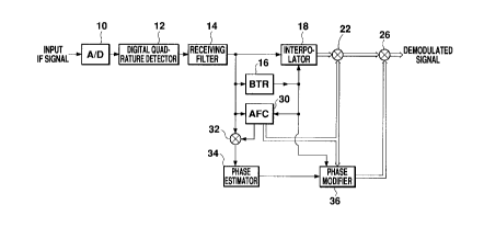
Embodiment 2
Fig. 2 is a block diagram showing the configuration of a
digital demodulator according to a second embodiment of the
invention. In Fig. 2, the components identical to those of
the first embodiment have identical reference numerals, and
are not described here.
In the second embodiment, the phase estimator, as well as
the AFC, is operated in response to signals generated at the
oversampling interval. The demodulator can operate at a
higher rate than the demodulator of the first embodiment.
Referring to Fig. 2, the AFC 30 calculates not only a
frequency deviation correcting signal for the decision timing
signal (generated at the sampling interval) but also a
frequency deviation correcting signal for the signal generated
by the digital quadrature detector 12 at the sampling
interval. In other words, the AFC 30 estimates the frequency
deviation ~ on the basis of the detected sample signal
outputted by the receiving filter 14 at the oversampling
interval. Further, the AFC 30 calculates the frequency
deviation correcting signal CINT (refer to Equation 10) for the
17
- 2180905
signals outputted at the decision timing, and the frequency
deviation correcting signal C~ (Equation 11) for the signals
outputted at the sampling interval.
CINT (mTs)=exp( j~mTs) -- (10)
C~(nT)=exp(~ mT) ------- (11)
The frequency deviation correcting signal CINT ( for
correcting the frequency deviation at the decision timing) is
inputted to the multiplier 22, while the frequency deviation
correcting signal C~ (for correcting the frequency deviation
during the sampling interval) is inputted to the multiplier
32.
The multiplier 22 complex-multiplies the decision timing
signal RN ( from the interpolator 18) by the frequency
deviation correcting signal CINT~ thereby eliminating the
frequency deviation component from the decision timing signal
RN. Thus, the multiplier 22 outputs a decision timing signal
XINT free from the frequency deviation component. The decision
timing signal XINT is expressed by:
XINT (mTS) RN (mTS) XeXP (--j~mTS)
={I(mTs)+jQ(mTs)}exp( j~N) ~~ ~ ~ (12)
On the other hand, the multiplier 32 multiplies the
detected sample signal (from the receiving filer 14) by the
frequency deviation correcting signal C~ so as to eliminate
the frequency deviation components from the detected sample
signal, thereby outputting a detected sample signal X~ free
21 80905
_
from the frequency deviation component, expressed by:
XRX (nT)=l IQC (nT)+jQQc(nT)}xCRx(nT)
={I(nT)+jQ(nT)}exp(j~ ---- (13)
The phase estimator 34 estimates an initial phase
component ~ in the detected sample signal on the basis of the
detected sample signal XRX (without the frequency deviation
component, and outputted at the oversampling interval). In
other words, the phase estimator 34 performs the phase
estimation on the basis of the signal XRX/ independently of the
output of the BTR 16. Then, the phase estimator 34 calculates
a phase correcting signal CPE2 on the basis of the estimated
initial phase component ~. The phase correcting signal CPE2 is
expressed by:
CPE2 (nT)=exp(-j~) -------- (14)
The phase correcting signal CPE2 derived by the phase
estimator 34 is used to correct the initial phase component 3
at the sampling timing. Therefore, this phase correcting
signal CPE2 cannot be used to correct the initial phase
component ~N Of the decision timing signal outputted by the
multiplier 22. This is because the phase components ~ and ~N
are different due to the difference between the start points
of the sampling timing and the decision timing.
In the second embodiment, the phase modifier 36 modifies
the phase correcting signal CPE2 to a value corresponding to
that of the signal generated at the decision timing.
Specifically, the phase modifier 36 calculates an amount of
phase rotation caused by a difference between the start points
2 1 80905
of the sampling timing and the decision timing, on the basis
of the decision timing information from the BTR 16 and the
frequency deviation information from the AFC 30. Then, the
phase modifier 36 modifies the phase correcting signal CPE2
based on the calculated amount of phase rotation, thereby
outputting, at the Nyquist rate, a phase correcting signal CPE3
for the signals outputted at the decision timing. This signal
CPE3 is expressed by:
CPE3 (mTs)=eXP( i~N) - - - - ( 15 )
The phase correcting signal Cp83 is inputted in the
multiplier 26, which multiplies the phase correcting signal
CPE3 by the decision timing signal XINT ( expressed by Equation
12 and free from the frequency deviation component), thereby
eliminating the frequency deviation component from the
decision timing signal. The multiplier 26 outputs a
coherently detected signal S, expressed by:
As can be seen from Equation (9), the digital demodulator
of this embodiment demodulates the in-phase component I and
the quadrature component Q in the original digital signal.
In this embodiment, not only the AFC 30 but also the phase
estimator 34 operate in response to the detected sample
signals generated at the oversampling interval, independently
of the operation of the BTR 16. Thus, both the AFC 30 and the
phase estimator 34 can operate before the stabilization of the
BTR 16, so that the digital demodulator stably operates in a
shorter time than the digital demodulator of the first
2 1 80905
embodiment.
Even when the BTR 16 malfunctions during the stable
operation of the digital demodulator, both the AFC 30 and the
phase estimator 34 can estimate the frequency deviation ~ and
the initial phase component ~, independently of the output
signal from the BTR 16. Therefore, the AFC 30 and the phase
estimator 34 precisely output the frequency deviation
correcting signal and the phase correcting signal,
respectively, immediately after the stabilization of the BTR
16.
The technique utilized in this embodiment is applicable to
the demodulation of not only the QPSK-modulated signals but
also signals such as BPSK- or FSK-modulated signals.
Embodiment 3: -
In a third embodiment, a digital demodulator operates on a
differential detection system, and is applicable to the
demodulation of phase-modulated signals.
This digital demodulator is configured as shown in Fig. 3,
in which the components identical to those of the first
embodiment are assigned by identical reference numerals, and
will be not described here.
The operation of the components between the A/D converter
10 and the interpolator 18 is the same as that of the first
embodiment. In this embodiment, phase information is
extracted from the decision timing signal outputted by the
interpolator 18, thereby performing the delay detection on the
basis of the phase information.
2 1 8090~
A coordinate transformer 42 transforms the decision timing
signal (expressed by Equation 5), outputted by the
interpolator 18, into the form of polar coordinates, and
determines a phase of the decision timing signal. The phase
~ of the decision timing signal is expressed by:
~(mTs)=~mTs+~N+~M(mTs) ~~~~~~~~ (17)
where ~M (mTs) iS a phase component resulting from the
modulation, and expressed by:
~M (mTs)=arg{I(mTs)+jQ(mTS)} ------- (18)
An output signal of the coordinate transformer 42 is
inputted in a delay circuit 44 and a subtractor 46. The delay
circuit 44 delays a phase signal ~ (outputted by the
coordinate transformer 42) by one symbol interval (i.e. one
Nyquist interval). In order to perform the differential
detection, the subtractor 46 subtracts the phase signal
((m-l)T9), which is delayed by one symbol period, from the
phase signal ~(mTs) of the coordinate transformer 42. The
subtractor outputs a differential-detected result signal
DD(mTs), which is expressed by:
DD(mTs)=~(mTs)-~((m-l)Ts)
=~M (mTs) -~M ( (m-l)Ts)+~Ts ~~~~~~ (19)
As can be seen from Equation 19, the differential-detected
result signal DD contains a phase rotation component ~T~
caused by the frequency deviation as well as the phase
component caused by the modulation. Unless the phase rotation
component ~Ts is eliminated, error rate characteristics will
2 1 80905
be degraded.
In order to overcome the foregoing problem, the AFC 40
calculates the phase rotation component ~T~, and the
subtractor 48 subtracts the phase rotation component ~Tc from
the differential-detected result signal DD. In other words,
the AFC 40 estimates the frequency deviation ~ on the basis
of the detected sample signal, which is outputted by the
receiving filter 14 at the oversampling interval. Then, the
AFC 40 calculates a phase rotation D~c per symbol interval
(i.e. the Nyquist interval) T~.
DAFC (mTq ) =~TS - - - - - - ( 2 0 )
The value of one symbol interval Ts is substantially well-
known, because T5 is approximately integer times as large as
the oversampling interval T. The AFC 40 stores a value, which
is determined by an oversampling clock, as a fixed value of
the symbol interval T~, so that the phase rotation DAFC can be
precisely drived (at a practically usable level) by applying
the fixed value to the Equation 20. In order to derive the
phase rotation DAFC more precisely, this embodiment may be
configured such that a more precise symbol interval T~ derived
by the BTR 16 is applied to the AFC 40.
The differential-detected result containing only a
modulated phase component can be obtained when the subtractor
48 subtracts the phase rotation DA~C from the differential-
detected result signal DD of the subtractor 46. An outputsignal SDE Of the subtractor 48 is expressed by:
SDE (mT~) =DD (mT3) -DAFC (mT~)
23
21 80905
_
~M(mT3) ~M( (m l)Ts) ....--- (21)
As can be seen from Equation 21, the output signal SDE of
the subtractor 48 precisely corresponds to a difference
between ~M(mTs) and ~M( (m-l)Ts) caused by the phase modulation.
In this embodiment, the AFC 40 operates independently of
the BTR 16, i.e. the AFC 40 can operate before the stable
operation of the BTR 16. The differential-detection
demodulator can operate at a high speed in this embodiment
Further, the AFC 40 can estimate the frequency deviation
~ regardless of the output signal from the BTR 16 even when
the BTR 16 malfunctions during the stable operation of the
digital demodulator. Thus, the AFC 40 can output a precise
signal indicative of the phase rotation as soon as the BTR 16
resumes its stable operation, which enables the whole
demodulator to return to its stable state.
The amount of differential detection is one symbol
interval in the foregoing description. Alternatively, it may
be several symbol intervals.
The differential detection may be performed by another
technique such as complex multiplication in place of the phase
subtraction in this embodiment. The phase detection using the
complex multiplication will be performed as follows.
In this differential detection, the output signals of the
interpolator are delayed, i.e. a current output signal and an
output signal of a prior symbol interval are subjected to the
complex multiplication. In this case, a differential-detected
result signal DD(m) is expressed as follows, when the
24
21 80905
_
interpolator outputs a signal S(m) at a time m.
DD(m)=S(m)xS*(m~ ---- (22)
where S*(m-1) is a complex conjugate signal of the output
signal S(m) at a time m-1. S(m) and S(m-1) are expressed by:
S(m)=A(m)exp{j~(n)}
S(m-1)=A(m-l)exp{j~(n-1)} ---- (23)
where A(m) is an amplitude component of the output signal
S(m), and ~(m) is a phase component of the output signal S(m).
The differential-detected result signal DD(m) is rearranged
by:
DD(m)--A(m)exp{j~(n)}xA(m-l)exp{-j~(n-1)}
=A(m)A(m-l){j(~(m)-~(m-1))} ---- (24)
It is understood that the phase difference which is caused
during one symbol interval can be derived by the complex
multiplication. Thus, a demodulated signal can be obtained by
eliminating the frequency deviation component from the phase
difference component.
Embodiment 4:
Fig. 4 is a block diagram schematically showing the
configuration of a digital demodulator according to a fourth
embodiment of the invention. In Fig. 4, components identical
to those in the third embodiment are assigned identical
reference numerals, and will not be described here.
The digital demodulator is a modification of the digital
demodulator of the third embodiment, and is intended to
accelerate the stabilization of the circuit operation when a
signal is received at an initial operation stage, and reliably
2 1 80905
`~
process the frequency deviation during the stable operation.
Referring to Fig. 4, the AFC 50 estimates a frequency
deviation ~ on the basis of a detected sample signal which is
outputted at the oversampling interval by the receiving filter
14. In response to a selection signal from a selector 52, the
AFC 50 calculates either the correction signal DAFC (i.e. the
phase rotation signal DAFC expressed by Equation 20) for the
subtractor 48 or a correction signal C~(nT)=exp(~ nT) for a
multiplier 54. Specifically, the AFC 50 calculates the
correction signal DAFC~ and supplies it to the subtractor 48
when the operation of the digital demodulator should be
quickly stabilized. On the other hand, the AFC 50 calculates
the correction signal C~ and provides it to the multiplier 54
during the stable operation of the digital demodulator.
The multiplier 54 is present between the digital
quadrature detector 12 and the receiving filer 14. The
correction signal C~ is fed back to the multiplier 54, which
eliminates the`phase rotation component (which is caused by
the frequency deviation ~) from the detected sample signal.
A received signal containing a large frequency deviation tends
to have a broad frequency band. In such a case, if the
frequency deviation is not eliminated, the receiving filter 14
may filter a modulating signal component. However, if the
correction signal C~ is fed back to the multiplier 54, the
frequency deviation component can be eliminated before the
signal is applied to the receiving filter 14. Thus, it is
possible to prevent the modulating signal component from being
26
- ` 21 80905
deleted. On the other hand, if the correction signal C~ is
fed back to the multiplier 54 immediately before the received
signal is applied to the receiving filter 14, it is difficult
to quickly stabilize the AFC loop because of time needed for
the receiving filter 14 to become stable. Thus, the digital
demodulator is not supposed to operate at a high speed.
This circuit configuration enables the digital demodulator
to quickly become active and stable, and to process a burst
signal or the like which is inputted at the initial operation
stage. In such a case, the digital demodulator can correct
the frequency deviation after the delay detection as in the
third embodiment. Further, once the digital demodulator
operates stably, the frequency deviation should be further
quickly corrected. This can be performed before the received
signal is applied to the receiving filter 14. Thus, even when
the received signal contains a large frequency deviation, it
is possible to prevent the elimination of the modulating
signal component, through the elimination of the frequency
deviation on the basis of the correction signal C~ before the
received signal is applied to the receiving filter 14. This
technique is also applicable to the digital demodulator of the
first and second embodiments.
In this embodiment, the digital demodulator can demodulate
the received signal appropriately in accordance with a
received state of the signal. Specifically, the digital
demodulator selects a mode in which the digital demodulator
operates at a high speed but the received signal is somewhat
27
21 80905
degraded by the receiving filter, or a mode in which the
digital demodulator operates at a low speed but the received
signal is not degraded extensively by the receiving filter.
For instance, the operation of the demodulator can be quickly
stabilized so as to receive the signal at its initial
operation stage, and then process the frequency deviation
extensively in its stable operation stage.
In the foregoing embodiments, the input IF signals are
subject to the analog-to-digital conversion, and then to the
digital, coherent and quadrature detection. The coherent
detection can be performed using another configuration in
place of the foregoing configurations. For instance, an input
IF signal may be subject to analogous, coherent and quadrature
detection, and a detected signal is subject to the analog-to-
digital conversion, as shown in Fig. 5. Referring to Fig. 5,the input IF signal is coherently detected by multipliers 102
and 104 on the basis of reference signals which are an output
signal of a locked oscillator 100 and a signal obtained by
phase-shifting the output signal by a ~/2 phase shifter 114,
respectively. The detected signal is waveform-shaped by low-
pass filters (LPF) 106 and 108, and is subject to the analog-
to-digital conversion by A/D converters 110 and 112. The A/D
converters 110 and 112 output detected sample signals I~ and
Q~ in response to clock signals which have been outputted at
the oversampling interval T and inputted in these A/D
converters 110 and 112. The oversampling interval T is equal
to the timing at which the digital quadrature detector 12
28
2 1 80905
outputs the signals in the foregoing embodiments. The
detected sample signal is equivalent to the signal outputted
by the digital quadrature detector 12. The digital
demodulator demodulates the received signal on the basis of
the detected sample signal.