Note: Descriptions are shown in the official language in which they were submitted.
218099
.~
TITLE: HIGH CURREL~T, LOW PROFILE l~JLIUl.:~OK & METHOD FOR
MAI~ING SArD3
R~rT~(:W~lr-~ OF T~E l~ n ~ lU
The present invention relates to a high aurrent, low
profile inductor and m~thod for making ~ me.
Inductors of this type are ref erred to by the
designation IELP which is an abbreviation for "inr~ t.~r, high
current, low prof ile . "
Most prior art indluctive ~ ~ are _ ~ ' of a
i-- core having a c-shape, and E-~hape, a toroidal
shape, or other shapes and c!onf;~r~Lt;~n~. Conductive wire
coils are then wound a~ound the ;~ core _ Ls to
create the inductor. These types of prior art ; ~ t~lr~
recluire numerous s~pAr~lte parts, ;n~ ;n~ tha core, the
winding, and some ~ort of DLLI~ ULe~ to hold the parts
t~, ~t h~r. Also, these inductive coils often hav~ a shell
~uLL~ ul.ding them. As a result there are many air ~p~lce~ in
the inductor which affect its op~-rA~ and which prev~nt~
the ' m; ~--t; l~1 of 8p~1Ce.
Therefore, a prim~Lry object of the pre~ent invention is
the provision of an; u..~d high current, low profile
inductor and method foI- m~Lking same.
A further object c~f the present invention is the
provision of a high culrent, low profile ;n~ t~lr which has
no air ~pace~ in the inductor, and which ;n~ A a magnetic
material . _let~ly ~u.Luul.ding the coil.
A further object ~f the pr~sent invention is the
provision of an; uv.:d high ~urrent, lc~w profile inductor
which in~-ln~ L closecl ;~ system which provide~ a self
13h; ~7 rl; n~J ~'ArAh; l; ty.
A further object of the present invention is the
provision of an; ,.~.1 high current, low profile; n~ tnr
which ~-s;m;~A~ the utll;7At;~n of the space needed for a
given inductance perfoL-mance 80 that the in~ t~r can be of a
minimum size. A furthe~ object of the present invention is
j~,. 218~g9~
the provision ofi an improved inductor which is smaller, less
expensive to manufacture~, and is capa~le of accepting more
current without saturating than previous inductance coils.
A further object ofi the present invention is the
provision of a high cur~ ent, low prof ile inductor which
requires fewer turns of wire in the coil to achieve the same
inductance achieved with larger prior art inductors, thus
lowering the series resistance of the inductor.
SUMMaRY OF THI~ lh~/c,~
The foregoing objects may be achieved by a high current,
low profile induetor whieh inrl~ a wire eoil having an
inner eoil end and an outer eoil end. A magnetie ~~trr;Al
c l~ ly ~u..vu,.~a the wire eoil to form an induetor body.
A first lead is c~nn~ r~t~3 to the inner eoil end of the eoil
and extends through the magnetie - ~r; ~1 to a f irst lead end
expo~ed out~id~ the; nrl~lrtr~r body. A seeond lead i8 eonneeted
to the outer eoil and es.tends through the , ;r 'r~r;Al
to a seeond lead end exposed outside the i n~3~rtr~r body.
Th~ method for making the i~ r ~ _ r-- forming a
wire eoil having an inn~r eoil end and an outer eoil end. A
f irst lead iB attaehed to the inner eoil end of the eoil . The
eoil i8 then wound into a helieal spiral. Then a seeond lead
is AttArh~r~ to the outel- eoil end. The first and seeond leads
eaeh havff f irst and seec~nd f ree end8 Next a E - ~1
tir '~r;~ e8~uL~s molded c l~tely ~round the
eoil 80 as to ereate an induetor body. The free ends of the
first and seeond leads ~-xtend outside the ;n~ rt~r body.
BRII~F Dl~:ic~ OF THE FT~ OF TH13 DRAWINGS
Flgure 1 is a pietorial view of an induetor eonstrueted
in ~ ;e with the present invention and mounted upon a
circuit bo~rd.
Figure 2 is A pictoriAl view of the coil of the induetor
and the lead frame whiell is at~s~rh~l to the eoil before the
molding process.
. ~ 2180~92
Figure 3 i8 a pictorial view of the inductor of the
present invention after the molding proceas is complete, but
before the lead frame i8 severed from the leads.
Figure 4 is a flow diagram showing the method for
constructing the inductor of the present invention.
Figure 5a i8 a sectional view of the lead frame and coil
mounted in a press.
Figure 5b is a top plan view of Figure 5a.
Figure 5c is a vie~ similar to Figure 5a, but showing
the powder ~LLL~ '; nq the lead frame and coil before
pl-__n~ ~ i8 applied.
Figure 5d is a vie~ similar to 5a, but showing the
es~.La being applied to the coil, lead frame, and powder.
Figurs 5e is a vie~ similar to 5a, but showing the
ejection of the lead fr~me and the molded inductor from the
mold .
Figure 6 is a pc_D~ ive view of a '{f{~d form of the
invention u~{l;7;nq a coil of wire having a round cro~s
section.
Figure 7 iB an oYrll o~lDd ~ ~;Live view of the lead
frame and coil of the d~vice of Figure 6 befor~ a~embly.
DRT1~TT Rn UISS~ OF TEIE ~ sv 1 ,n~
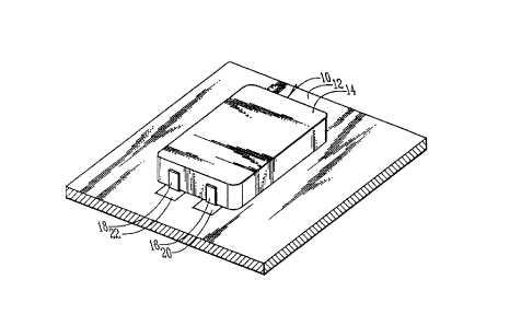
Referring to the rllrAwinq~ the numeral 10 g~n~r/~l ly
de8ignates the high cur~:ent, low profile ;- nr (I~P~ of
the present in~ention. IEILP 10 i~ shown in Figure 1 to be
mounted on a circuit bonrd 12 . IEILP 10 i n~ an; n~ tnr
body 14 having a first Lead 16 and a second lead 18 c~ n~l{
out~-r~ily th~Lt:LL~ . Th~ leads 16 and 18 are bent and folded
under th~ bottom of the i n~ tor body 14 and are 3hown
soldered to a first pad and a second pad 20, 22 respectively.
Referring to Figure 2 thQ inductor 10 is construc~ted by
forming a wire coil 24 from a flat wire having a rect~n~.lnr
cross section. An example of a preferred wire for coil 24 is
an enameled copper flat wire r~-nllf~tllred by El.P. Reid
Company, Inc., 1 r~ ue Boulevard, P.O. Box 352 440, Palm
Coast, Florida 32135, tlle wire is made from OFEIC Copper 102,
2180992
99.95% pure. A polymide ellamel, class 220, coats the wire for
insulation. An adhesive, epoxy coat bound "E" is coated over
the insulation . The wire is f ormed into a helical coil, and
the epoxy adhesive is actuated by dropping acetone on the
coil. Activation of the epoxy can also be done by heating the
coil. Activation of the adhesive causes the coil to remain in
its helical c~nfirrlration without loo~--nin~ or unwinding.
Coil 24 i nol l-Ao~ a p Lur~llity of turns 30 and al~o
i n~ o~ an inner end 26 lnd an outer end 28 .
A l~ad frame 32 formed of r - ~ ~ bronze, S10 alloy,
which i8 one half hardened, in~ Ao~ first lead 16 which has
one end 34 welded to the inner end 26 of coil 24. Lead frame
32 also i nrl U~109 a second lead 18 which has one end 38 welded
to the outer end 28 of coil 24. Leads 16 and 18 include free
ends 36, 40 which are shoiin to be attA~ h~l to the lead frame
32 in Flgure 2. The weldillg of ends 34, 38 to the inner end
26 and the outer end 28 oE coil 24 is preferably - _ 1; ~ho,
by a resist~nce welding, Ibut other form~ of ~ r; ng or
welding may be u~ed.
P-f~rr;n~ to Figure~ sa and 5b, a pl~ ~ molding
machine 68 in~ 3o~ a platten 71 having a T~ lead frame
holder 70 in i~Atin`r~ with a rectangular di~ 72. Platten
71 is slidably mounted for vertical sliding .G ' on slide
posts 74 and is spring mo1nted on those posts 74 by means of
springs 76. A base 78 includes a ~tationary punch 80 which
project~ upwardly into th~e rectA"~l~r die 72 as shown in
Figure 5a.
The lead frame and c~Dil assG-mbly shown in Figure 2 is
placed in the T- ~r ~ le~d framG~ holder 70 as shown in
Figures 5~ and 5b. In this position the coil is spAced
slightly above the upper end of st~t i~nAry punch 80 .
Referring to Figure 5c a p ~ Gd molding l-~tor;~l 82 is
poured into the die 72 in such a manner a~ to completely
~uLLuul-d the coil 24. The leads 16, 18 extend outwardly from
the L- - ed material 82 where they are connected to the lead
frame 32 .
~ 2180992
The magnetic molding material is comprised of a first
powdered iron, a second powdered iron, a filler, a resin, and
a lubricant . The f irst and second powdered irons have
dif f ering electrical characteristics that allow the device to
have a high inductance yet low core losses 80 as to maximize
its ~-ffi~ n-~y. Example1 of preferred p~ ed irons to use
in this mixture are as follows: a powdered iron manufactured
by ~eqA~--- Company, Ri.ver Road and Taylors Lane, Riverton,
New Jersey, under the trade riD~i~n~ti~n Ancorsteel lOOOC.
This 1000 C r~-t~riAl is in~--lAted with 0.4896 mass fraction
with 7596 H3P04. The secc~nd ~ --n~ -;A1 ig manufactured
by BASF Corporation, lOt~ Cherryhill Road, pAr~irpAny~ New
Jersey under the trade ~ i qnAt i ~n Carbonyl Iron, Grade SQ.
This SQ material is i - 1 At-~ with 0 . 87596 mass fraction with
75% H3P04.
The p ~ad _ i,, r-t-~r;J~l algo ;n~ a filler,
and the pr~.,...d fille~. i8 f..1..._l by Cypru~ Induntrial
M;n~rAl~ Company, Box 3299, Tnq~l 1, California 80155 under
the trade. ~~ qr~ n Snowflake PB. This i8 a calcium
cArhr~nAte powder.
A polyester resin iLs also added to the mixture, and the
pLt:fe..- d resin for thiLI purpos~ is ~r.u~ _LUL~-1 by Morton
International, Post OffiLce Box 15240, Reading, Pennsylvania
under the trade ~e-~; qnA~ n Corvel Flat Black, Number 21-
7001 .
In Arl~i i t; on a lllhrl ~-Ant is added to the mixture . The
lllhri~'Allt i8 a zinc gtearate .,~ u~c_Lu-- d by Witco
Corp-~r~t; ~n, Box 45296, Huston Texas under the product
nAt;~7n T--hr~7;n~ Wl
Various combinatiolls of the above ingredients may be
mixed togetb~r~ but the preLe..~d mixture is as follows:
1,000 grams o~E the first ~ -ed iron.
1,000 grams oE the 8econd F .:d iron.
36 grams o~E the filler.
74 grams o E the resin.
O . 39~ by weight of the 1 llhr;, Ant .
The above materials (otller than the lllhr;-~nt) are mixed
together and then acetolle is added to wet the material to a
-- 2180982
mud-like consi~tency. The material i~ then permitted to dry
and iB Ei~;L~elled to a particle size of -50 mesh. The 1 llhri ~ Ant
is then added to complete the material 82. The material 82 is
then added to the die 72 as shown in Figure 5c.
The next step in the process involves the forcing of a
movable ram 87 downwardly onto the removable punch 84 50 as
to force the punch 84 into the die 72. The force exerted by
the removable punch 84 should be appr~ ;~^tsly 15 tons per
square inch to 20 tons per square inch. This causes the
r ..: ~d ~-~r~Al 82 to be ~ and molded tightly
let~ly around the coil 80 as to form the inA~ f~r body 14
shown in Figure 1 and in Figure 5e.
Referring to Figure 5e an ejection ram 86 is lowered on
to pl~tten 71 80 as to force pl~tte~ 71 ~' rAly against
the bias of springs 76. This causes the stAt;~nAry ram 80 to
~ject the molded assembly from the die 72. At this stage of
the production the molded assembly is in the form which i8
shown in Figure 3 . The molded ~ 1; r~ are then baked at
325-P for one hour and forty-five minutes to set the
polyester resin.
The next step in the LuLing process is to severe
the lead frame 32 from the leads 16, 18 along the cut lines
42, 44. The leads 16, 18 are then bent downwardly and
inwardly 80 au to be folded against the bottom surface of the
inductor body 14.
Th~ variou~ step- for forming the inductor are nhown in
block diagram in Figure 4. Initially one of the wir~ ends 26,
28 is w~lded to it~ C;VLL~ L ';ng end 34,36 of leads 16, 18
aB L~ A by block 45 . Next the coil i~ wound into a
helix as shown by block 46. Block S0 L~L~e_.l88 the step of
welding the other end 26, 28 to its COLL`-,L~'~nA;n~ lead 16,
18. The coil wire in~ A~-I an epoxy coat of bonding I ,-ri
A~ri hod above. A bonding 8tep 49 is achieved by applying
the acetone 48 or heat to cause the bonding material to bind
or adhere the various turn8 30 of coil 24 togethGr.
Next, at step 52 the p_ ~d magnetic material is mixed
to~eth~r adding ingredi~nts 54, 56, 58, 60, and 62.
``-- 21809~2
The pressure molding step 64 involves the application of
pL~=s~uL~ as shown in Figures 5a through 5e. The parts are
then heated to cure the resin as shown in box 65.
Finally after the curing is complete the bending and
cutting step involves cutting off the lead frame 24 and
folding the leads 16, 18 against the bottom surface of the
inductor body 14.
When compared to other inductive ~ the I~LP
inductor of the present invention has several unique
attributes. The cnn~rt;ve winding, lead frame, _ ;c core
~-t~-r;--1, and protective ~nr10sure are molded as a single
;nt~-JrA1 low profile unitized body that has t~rm;r~-t;t~n leads
suitable for surface i n~. The construction allows for
mAximum nti 1 i~t;nn of available space for _ ;~
p_LLc ~ and is ;<~nl ly 8elf 8h;e1~;ng.
The unitary ~ LLu- l ion ~l im~ te~ the need for two
core halves a~ was the c~e with prior art 8 corel~ or other
core ~hapes, and al~o ~1 ;m~n-t~ the r-- ~ 'At~d assembly
labor .
The unique conductoc winding of the present invention
allows for high current opora~;on and also op~;m;--q _agnetic
p~ ~r8 within the indluctor ~ foo~rr; n~
The manufacturing pcocess o~ the pre~ent invention
provides a low cost, high p~ ~ ~ package without the
L~nA~nre on expen~ive, tight tol~r~-n-~e core ~r;Al- and
~pecial winding t~ ; qu~
The ; 1~ core ~r; ~ 1 has high resistivity
t ~ ; n~ 3 mega ohms ) t hat enable~ the induetor as it is
manufactured to perfor_ without a eonductive path between the
surface mount leads . The magnetic ~t--r; ~1 also allows
ef f; ri~nt op~rAt; on up tc 1 MElz . The inductor package
~_LLoL~ance yields a low DC resistance to inductance ratio of
two m;ll;n' per miuLolR.lLy. A ratio of 5 or below is
c nn ~ ~ red very good .
Ref erring to Figures 6 and 7 a ~; f; ed f orm of the
invention is ~ i gn~t~d by the numeral 88 . Inductor 88 is
formed from a coil 90 of wire having round cross section. The
`-- 21809~2
coil 90 includes a fir~t coil end 92 and a second coil end
94. A lead frame 96 in~ a first lead 98 and a second
lead 100 having first a~d second lead ends 102, 104.
The method of assembly of device 90 is different from
the device 10 shown in Figures 1-5. With device 90, the coil
ia wound f irst and is heat bonded during winding . Then the
coil ends 92, 94 are welded to the lead ends 102, 104
respectively. The mixed p ~1 r-t--r; nl is then applied and
the pressure molding process is e 1 i ~h--~ in the same
fashion as described before. FiQally the leads 98, 100 are
cut of f and bent downwardly under the bottom of the device
10 .
The position of thl leads 98, 100 can be varied without
detracting from the inv~ntion. Also, it is pos~;hlf~ to put
more than one coil withi n a molded part . For example, it
would be pos~; hl~ to put two or more coils 24 within th~
molded body 10 or two or more coils gO within the lded body
88.
In the rlr~ andL ~r~;f;~ there has been set
forth a ~ e~ '; of the invention, and although
8Fe~'; f i 1~ terms are employed, these are used in a generic and
descriptive sense only emd not for ~_ ~oEas of limitatio~.
Changes in the form and the proportion of parts as well as in
the substitution of eguivalents are c^nt~ 1 nted as
circumstance- may suggest or render ^Ype~ 'nt without
depArting from the spirit or scope of th~ invention as
further defined in the ~oll~ -;n~claims.