Note: Descriptions are shown in the official language in which they were submitted.
2181~50
WO 96/18250 . ~
METHOD, t)EVlCE, ~IND RADIO FOR COMPENSATING FOR
MODULATOR FREQUEIICY DRIFT WHILE ALLOWING FOR DATA
TRANSMISSION
s
Field of the Invention
The present inventlon relates generally to l,di~s",iLI~r
modulators used in half-tiuplex frequency modulated communication
10 systems, and more particularly to corrlpensating for modulator
frequency drift while allowing for data trans",issioll.
Background of the Invention
A 1, a~ilional metho~i of generating constant-envelope
frequency shift keyed, FSK, data modulation employs a phase-locked
loop, PLL, to maintain the frequency of an ~Cso~ d voltage
con~,ulled oscillator, VCO, with its stability derived from the PLL's
20 reference frequency. The PLL's frequency reference typically
consists of a crystal oscillator. Data is applied to the VCO which
then provides the FSK modulation. This method has the capability of
sustaining fairly high levels of frequency deviation as co""~d.t:d to
the older technique of dilrect frequency modulation of a crystal
25 oscillator. This capabilit~ is i~pulldrll in moderate to high data
rate systems where the ~requency deviation is typically an
appr~cidL,lc fraction --e.g., 25 Y~- of the data rate. In combination
with a frequency offset l-dnsc~îv~r architecture, the PLL is capable
of accurate and stable operation over a wide range of operating
30 frequencies.
A problem that commonly occurs with PLL rrlo~ in data
systems relates to the loop bdl~u~ lll. While data that has
frequency content sulJ:,Idllli~'~y above the loop bal,d~ l, is able to
35 modulate the VCO s~ ,r;ly, if there is frequency content that
falls inside the loop bal,~ l,--such as that which occurs with
WO 96/18250 2 1 8 1 0 5 0
long strings of zeros or ones--destructive distortion of the data
stream will take place which will render the data unrecoverable by
an intended receiver. This issue has been add,t:ssed in various ways.
Some methods employ a dual-port modulation scheme. This approach
5 extends the PLL response towards direct current, DC but never quite
reaches it because of dynamic range li",i~alio~,s of some element of
the loop. Other methods use complex schemes that read incoming
data and ~ Uyldlll loop dividers to achieve a DC response. Still
other methods are ~t:Cor, ~ to the high-pass response of the PLL
10 frequency modulator and use data ~ "~,x" that randomize data to
deal with long strings of zeros or ones, but still have to contend
with vexatious patterns that frequently confound such attempts.
There exists therefore a need for a method device and radio
15 for compensating for modulator frequency drift while allowing for
data l~dns",;.,sion, wherein the method and device is sULI~Ldll'- '1)1
less complex than prior art.
Brief Desr.,i,u~ion of the Drawings
FIG. 1 is a flow diagram of one e",L,od;",e"l for implementing a
method for co""~el~sali"g for modulator frequency drift while
allowing for data l,dnsl";ssiol, in ac~iordance with the present
25 invention.
FIG. 2 is a flow diagram, shown with greater detail of the step
of adjusting the premodulation signal of FIG. 1 in acc~,~ance with
the present invention.
FIG. 3 is a block diagram of one ~",L,o,ii",e"l of a device which
Co"",ellsdl~s for modulator frequency drift while allowing for
simultaneous data l,di~s",;ssion in acco,dance with the present
invention.
WO961187~50 21 81050 r~ 7
FIG. 4 is a block diagram, shown with greater detail, of the
adjusting circuit of FIG. 3 in accor-ld~e with the present invention.
FIG. 5 is a diagram of one embodiment of a radio utilizing a
S device which ct;r",uallsdIas for modulator frequency drift while
allowing for data lldns",;ssion in acctj,~ance with the present
invention .
Detailed Des~ Iion of a Preferred El"bod;",t:"I
Generally, the present invention provides a method, device, and
radio for col",uel~sdIirlg ft)r modulator frequency drift whiie allowing
for data Lldi,sl,~ission in a half-duplex frequency modulated
15 communication system. An input signal is adjusted in such a way
that, when passed through a frequency modulator to provide a
lldns",ill~r excitation signal, frequency drift is negated. During
frequency training, the l,dr,;,",illt:r excitation signal passes through
a switch to a demodulator. The demodulator output is averaged and
20 used in the original adjustment. With such a method and system,
frequency drift is ctj""~ensdl~d with much less COIII~ A;lY ctj"".a,ed
to previous techniques.
The present inventia,n is more fully described in FlGs. 1 - 4.
25 FIG. 1, numeral 100, is a flow diagram of one embodiment for
implementing a method of ctjl"~ al-sdli"g for modulator frequency
drift accol," ,9 to the present invention. The modulator in this case
is a frequency modulator and consists of a free-running signal-
controlled oscillator with an external terminal for controlling its
30 frequency. Examples of signal-cor,I,.'' :' OSCilldlul:~ are a voltage
controlled oscillator, a current ctj"l,."s~ oscillator, and an
optically controlled oscillator. The voltage controlled oscillator
(VCO) is the most common. By itself, a VCO is i"l,i"sically capable
of being modulated by a wide range of frequencies including DC--
3s which is the desired behavior. The VCO is, however, also subject to
operating frequency drift which would make its use unsuitable for
WO96118250 2181 050 r~ J,
many ~ o~s. To solve this problem the input which carries
the ill~Ulllldli~l- to the modulator, which is called the premodulation
signal is adjusted by a modifier applied through a combiner to form
an adjusted premodulation signal (102). The adjustment can also be
5 made in the absence of data. Where the modulator has sufficient
frequency tuning range available through its external control
terminal, the overall effect of passing the adjusted premodulation
signal through the frequency modulator (1û4) is the provision of the
l,di,sl"i;l~r excitation signal which is the required frequency
lO modulation spectrum with a center frequency that is sufficiently
r l; l~t~hle by means of the modifier to co"",e"~dl~ for any
frequency drift encountered from the modulator. The training period
is initiated by a training c~"""al,d in response to several
predt:l~"" ,ed variables satisfying the training criteria (106). The
15 p,ed~ "";"ed variables may be a specific elapsed time since the
last training period, the physical hardware changing temperature a
specific amount, the absence of a received signal in
imple",e"~dlions where the d~u,~",e"lioned demodulator additionally
serves in a receiver function or any other user-defined training
20 schemes. The training controller accepts and p~uce3ses the
variables related to the training criteria and issues a training
cor"",alld when the criteria are met. The training CGlllllldl)~, in
addition to initiating the training period simultaneously closes a
switch (108) to apply the l,d":.""~lel excitation signal to the
25 demodulator to provide the demodulator output. The demodulator
output is then averaged (110) to provide an average demodulator
output which pertains to a measure of the average of the signal
applied to the demodulator.
There are three types of modifiers used to form the adjusted
premodulation signal (102). A ~ d~ lll ,ed modifier is used at
startup and may, for example be a factory-set level that places the
frequency modulator operating frequency at a convenient nominal
value as a starting point for further updating. Alternatively, the
predetermined modifier may be d~ lll. ,ed by the temperature of
the physical hardware r~ "ci"g a lookup table. An updated
1 50
W096/18250 2 1 8 0
s
modifier is used during a training period in response to a training
co"""and from the trainin~ controller and is d~""i"ad by the
average demodulator output. A stored updated modifier is used for a
majority of the time in the normal operation of the l,dnsc~:ver is
5 the value of the updated modifier at the conclusion of the training
period and is the value that tunes the modulator to the desired
frequency of operation.
FIG. 2 numeral 200, is a flow diagram, shown with greater
10 detail, of the step of adjusting the premodulation signal of FIG. 1 in
acc~,.ldilce with the present invention. A modifier is the
predetermined modifier at start-up the updated modifier when the
training cG"""and indicates or the stored updated modifier when the
training co"""a,~d indicates (202). The modifier is held and is
15 combined with the premoclulation signal to provide the adjusted
premodulation signal (204) When a training period is initiated by a
training co",l"and from the training controller the updated modifier
and an error pdldlllt:~a~ are provided by COIll~dlill9 the average
demodulator output to a pr~:d~ ", l~d reference level (206). The
20 error parameter is co""~a(ed to a plt:d~ llll ,ed error level (208). If
the error pa,d",t:lar is greater than or equal to the p,~d~ ",;"ed
error level, the updated m~difier is held and passed to the combiner
and the training period continues (212). Typically the modifier will
be an i"~r~",e"Ldl DC offset that is added to the premodulation
25 signal with a summing circuit. The center frequency of the
frequency modulator will change due to the adjustment to the
premodulation signal. The average demodulator output is again
cor"~.a, :d to a pred~"" ,ed reference level to provide a new value
of the updated modifier. Several sequential values of the updated
30 modifier may be generated in any particular training period as the
modulator compensation method converges to provide a minimal
error between the average demodulator output and the desired
~ alel-ce. This will cause the center frequency of the frequency
modulator to be within a known maximum error of a desired
35 reference frequency. Since the modifier is held constant when
combined with the premo~ulation signal the low pass response of a
~ 2181050
WO 96/18250 ~,IILI~,~
PLL is avoided and DC l,dll:.",;s:,;on is possible. If the error
pd,d",~l~r is less than the predetermined error level the last
updated modifier is held as the stored updated modifier (210) and
the training period ends.
s
The pled~ ", ,ed reference level can addiliol--'ly be updated
with a lookup tabie indexed to a variable such as temperature or
operating voltage if the reference of the demodulator is expected to
change and the reldliol1si, is known.
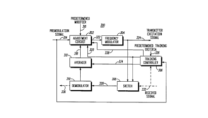
FIG. 3, numeral 300 is a block diagram of one ~",~c "~"l of a
device which compensates for modulator frequency drift while
allowing for simultaneous data lldl~s",;ssio~ in accon~di,ce with the
present invention. The device is cor"p,i~ed of an adjustment circuit
15 (302) a frequency modulator (304), a training controller (306) a
switch (308) a demodulator (310) and an averager (312).
The adjustment circuit (302) receives the premodulation
signal (314) and based on a training command (320) from the
20 training controller (306), applies either a p,~d~ ""i"ed modifier
(316), an updated modifier or a stored updated modifier to provide
an adjusted premodulation signal (322). This device operates with
the premodulation signal being either l,ans",ill~d data or the
absence of ll~u~s~ d data-- i.e., a quiet period. The adjusted
25 premodulation signal (322) is passed through the frequency
modulator (304) to provide a l, dns" ,illt:r excitation signal (324) .
The frequency modulator (304) typically is one of the following
signal-controlled ss t~r~: a voltage controlled oscillator, a
current conl,Jl-e~ oscillator or an optically co"l,~' ed oscillator.
30 The training controller (306) receives and uses training criteria
(326) and where selected, a received signal (332) to determine
when to send the training c~"""and (320) to the switch (308) and to
the adjustment circuit (302). The training controller would
typically be a ~ uplucessor or digital signal prr,cessor that
35 controls the functions of the overall radio. The switch (308) passes
the l,dns",ill~r ex~ lion signal (324) to the demodulator (310)
2181050
W0 96/18250 r~
when indicated by the trail1ing cu,,,,,,a~d (320). The demodulator
(310) uses the switched ll~l~sl"iLIt, ex~;iL~Iion signal (328) to
provide a demodulator outl~ut (330). The averager (312) receives the
demodulator output (330) and the bits indicator signal (334) ~rom
5 the training controller ~306). The averager (312) may include a
maximum peak detector and a minimum peak detector. When data is
present on the premodulation signal (314), the demodulator output
(330) will not be a constant value, but will have positive and
negative swings about its Imean due to the positive and negative
10 frequency d~vic-lions about the frequency modulator's (304) center
frequency resulting from the data modulation. The peak detectors
will capture the peak values and average them to provide the average
demodulator output (318). The peak detectors may be simple diode
detector circuits, and the minimum and maximum peaks may be
15 averaged with either a resistive network or an operational amplifier
summer circuit. If the modulation format requires that ex~ensh/c
filtering be applied to the data, as with 0.2 Gaussian Minimum Shift
Keying, GMSK, for example, sufficient time must be allowed to
ensure that a sufficient number of data bits are sequentiaily all
20 'zeros' and all 'ones'. The training controller (306) monitors the
premodulation signal (314) and indicates to the averager (312) with
the bits indicator signal (334) when a sufficient number of data bits
are sequentially all 'zeros' and all 'ones'. This permits the data
filter and any other filtering present in the demodulator to settle,
25 and the peak detectors then return values cor~ , " ,9 to maximum
negative and positive devi,Rtion about the center frequency of the
modulator. When data is not present on the premodulation signal
(314), the demodulator output (330) is a steady value ,~:~rt~ "li,~g
the frequency modulator's (304) center frequency and the maximum
30 and minimum peak detectors return the same value. The average
demodulator output (318) is an input to the adjustment circuit
(302).
The training period is initiated by a training cG"""and in
35 response to several pl~:del~r" ,edl variables satisfying the training
criteria (326). For example, the training criteria (326) may be based
WO 96/18250 2 1 ~ 1 0 5 0
on an elapsed time since last training a change in temperature an
absence of received signal, or a user dl::l7_1111 "3d training scheme.
The temperature change can be detected with a thermistor
monitored by the training controller. The demodulator (310) may be
S coupled to receive the received signal (332) for data recovery when
the device is not being trained. In this case, the training controller
may look for an absence of received signal before initiating the
training period so that incoming data is not lost.
FIG. 4, numeral (400) is a block diagram shown with greater
detail of the adjusting circuit for FIG. 3 in acc~,~d,~ce with the
present invention. The adjusting circuit (302) c~",yrises an updated
modifier calculator (406) a hold circuit (404) and a combiner (402).
The updated modifier calculator (406) c~",~.a,~s, the average
demodulator output (318) to a predetermined reference level (408)
to provide the updated modifier (410) and also an error parameter
(338) that is read by the training controller. The updated modifier
(410) is i"~;,eased when the average demodulator output (318) is
20 less than the ple:de:L~ "":.,ed reference level (408) and decreased
when the average demodulator output (318) is greater than the
pred~er",i"ed reference level (408). The hold circuit (404) passes
the predetermined modifier (316) to the combiner at start-up. If the
error parameter read by the training controller is not minimal, the
25 training controller signals the hold circuit to pass the updated
modifier to the combiner. If the error pa,d",t:l73r is minimal the
training controller signals the hold circuit to hold the updated
modifier as the stored updated modifier. The hold circuit ~nay be a
digital-to-analog converter (DAC). The combiner (402) combines the
30 modifier (412) with the premodulation signal (314) to provide the
adjusted premodulation signal (322). The pred~ "" ,ed modifier
(316) may be a factory-set level. The updated modifier is based on
the average demodulator output (318). The stored updated modifier
is a value of the updated modifier at the conclusion of a training
35 period.
2181050
W0 96/~82S0 I ~
FIG. 5, numeral 50~, is a diagram of one tlll,bo~;."~"L of a radio
(502) utilizing a device 1(300) which co""~e,~sdl~s for modulator
frequency drift while allowing for data l,al,~");~-:,ion in accu,dance
with the present inventioll. The device (3(.70) receives the
5 premodulation signal (31~) and provides an antenna (504) with the
lldl~lllilLt:l ex~,itdlioll sigl-al (324). The device (300) also receives
the received signal (332) to produce the demodulated received signal
(336). In addition to producing the demodulated received signal
(336), the device (300) efficiently uses the demodulator (310 in FIG.
10 3) to produce the demodl~lator output (330 in FIG. 3) to cc""~.~"sdle
for modulator frequency drift while allowing for data lldl~SII~;SSiOIl.
The efficiency of the device is desirable since the present invention
provides a reduced radio size, an i"1,uo,ldr,l customer s,,li~r~[ ~ion
feature.
Thus, the present i~7vention provides a method, device, and
radio for compensating l`or modulator frequency drift while allowing
for data ~,a,~s",;~3;0n. An input signal is adjusted in such a way
that when it is passed through a ~requency modulator to provide a
20 transmitter eAcildlioll signal, frequency drift is negated. During
training, the L,dilsn,itl~t e~,ilalioll signal passes through a switch
to a demodulator. The demodulator output is averaged and used in
the original adjustment. ~Nith such a method, device, and radio a
frequency drift is compensated for with much less c~""~le,.iLy
25 co""~a,~d to previous l~-,I,n, ~es
Although exemplary ~ Lc' .l~, are described above, it will
be obvious to those skille.d in the art that many alterations and
",o~ -ns may be made without departir7g from the invention.
30 Accul~illyly, it is intende~ that all such dll~,d~i~ns and
",odiriudlions be included within the spirit and scope of the
invention as defined in the appended claims.