Note: Descriptions are shown in the official language in which they were submitted.
CA 02181092 2005-03-07
- page 1 -
METHOD AND APPARATUS FOR CONTROLLABLY GBNBRATING SPARKS
IN AN IGNITION SYST~i OR THE LIKB
Field of the Invention
This invention relates generally to spark
generation and more particularly to a method and apparatus
for controllably generating and shaping sparks in an
ignition system or the like.
Background of the Invention
Solid-state ignition systems are known in the
art. U.S. Patents 5,065,073 and 5,245,252
teach, inter alia, that improved control over the
performance of an ignition system can be achieved by
incorporating a solid-state switch into an ignition output
circuit. As taught by these patents, the ability of a
solid-state switch to be triggered at a precise time
allows an ignition system incorporating such a switch to
achieve controlled spark rates. It also allows such a
system to generate time-varying spark sequences. In
addition, as explained in the above referenced patents,
since a solid-state switch, can be controlled independently
of the voltage level of the ignition system s tank
capacitor, an ignition system incorporating a solid=state
switch can be used to deliver various amounts of energy by
triggering the solid-state switch when a voltage
associated with a desired energy transfer appears across
the tank capacitor. This Later effect cannot be achieved
in older circuits using spark-gap switches since such
switches fire only at a single voltage which i.s preset
during manufacture of the spark-gap switch and will, thus;
fire as soon as the voltage across the tank capacitor
reaches the preset triggering level.
The '073 and 252 Patents also teach the
desirability of waveshaping the current delivered into an
218i09~
- page 2 -
igniter plug for a sparking event. For example, these
patents teach that it is desirable to deliver a current to
an igniter plug which initially increases at a low rate
while ionizing the plug's gap and thereafter increases at
a higher rate to sustain a spark across the ionized gap.
Among other things, controlling the rise time of the
current in this manner maximises the life of the
solid-state switch and the igniter plug by providing such
components an opportunity to pass through their transiticn
states before being taxed with a full, high energy pulse.
As mentioned above, prior art circuits such as
those disclosed in the '073 and 252 Patents have achieve3
some degree of control over spark generation. However,
prior art circuits such as these, while achieving many .
beneficial effects, have been somewhat constrained in
their ability to control spark generation by certain
physical limitations. For example, it is well known that
the energy stored in an ignition circuit employing a tank
capacitor is described bx the formula:
Energy = 1/2 * Capacitance * (Voltage)Z
Thus, the energy delivered by such a circuit can be varied
by changing either the charging voltage placed across the
tank capacitor or the capacitance of the tank capacitor
itself. There are, however, several practical limitations
involved in varying these characteristics. For example,
lowering the voltage levels used in the circuit requires a
disproportionately large increase in the physical size of
the capacitor used in. the circuit to achieve similar
energy levels. On the other hand, the available selection -
of capacitors, insulation materials, and solid-state
switch components becomes limited at higher voltage
levels.
The capacitance of prior-art spark generating
circuits is generally fixed when those circuits are
constructed. In a circuit which uses a spark-gap switch
the voltage is also fixed by the choice of the gap s
breakdown voltage. Thus, traditional spark generating
~1~~~9~
- page 3 -
circuits are designed to deliver a predetermined energy
level, but that energy level is thereafter unadjustable.
In addition, prior art circuits have not attempted to
control the plume shape of sparks generated at a spark,
generating device.
Ignition systems have been-constructed for use
as test apparatus wherein the user can manually vary the
energy delivered by the system by physically connecting or -
disconnecting multiple capacitors to achieve various total
capacitance and, thus, various total stored energy.
However, from a safety standpoint, the high voltage and
current levels in this part of the circuit makes
physically switching capacitors in or out of the circuit
somewhat impractical; usually requiring power-down and
physical reconnection before sparking can continue. In
addition, these systems have been limited to adjusting the
total energy delivered and have not provided any spark
shaping capabilities or real time control over the
intensity and shape of tile sparks generated.
pl~iects of the Iaventioa
It is a general object of the invention to
provide an improved method and apparatus for shaping and
controlling sparks. More specifically, it is an object of
the invention to provide an improved method and apparatus
for controllably generating sparks wherein both the energy
level and the profile over time of an energy pulse used to
generate sparks at a spark generating device can be
electronically adjusted to suit a given application.
It is another object of the invention to provide
an apparatus which electronically switches multiple
discharges into a common output for the purpose of
creating an ignition spark event at a spark'generating
device. It is a related object to provide an apparatus
wherein the total energy delivered to a spark generating
device is the additive contribution of multiple discharge
circuits. It is a related object to provide an apparatus
- page 4 -
which more reliably generates a significantly higher total __
energy output pulse than prior art circuits by using
multiple independent discharge circuits which individually
generate relatively lower energy outputs that are combined
to achieve a high energy output pulse rather than
increasing the stress on a single larger energy circuit.
It is another object of the invention to provide
an apparatus which can deliver a specific level of energy
to a spark generating device by intentionally discharging
only a subset of the multiple discharge stages. It is a
related object of the invention to provide an apparatus
which selectively combines the outputs of two or more
discharge stages having various output energy levels to
generate final output pulses having a wide range of energy
levels.
It is another object to provide an apparatus
which employs a binary weighting of the values of the tank
capacitors of the discharge stages to provide a greater
variety of possible output energies.
It is yet another object of the invention to
provide an apparatus which permits a user to adjust the
voltages) of the tank capacitors in the individual
discharge stages to scale their energy levels. It is
another object to provide an apparatus which permits a
user to both adjust the voltages) of the tank capacitors
in the individual discharge stages and to select which
stages to trigger thereby increasing the range of possible
output levels so that.output pulses having virtually any
energy level (zero to maximum) can be generated.
Another object of the invention is to provide an
apparatus which actively waveahapea its output pulse by
.timing the discharging of-several discharge stages so that
a pattern of overlapping, partially overlapping, or
non-overlapping discharges form a waveshaped pulse for
generating a spark having a given plume shape. It is a
related object to provide an apparatus which generates an
electrical waveform that imparts various characteristics
.~ ~18~~92
- page 5 -
to the physical time-varying shape of the spark plume
created at a spark generating device.
It is still another object of the invention to
provide an ignition system which achieves better ignition
by optimizing the spark plume for best transferring its
energy into the fuel mixture.
Another object of the invention is to provide a
spark generating apparatus whose operation enhances the _
life of an associated spark generating device by
controlling the spark plume to reduce the arc-induced
erosion of the spark electrodes. It is a related object
to provide an apparatus which ionizes the gap of a spark
generating device to form a plasma using a small energy
pulse, and then later delivers the remainder of the energy ,
to the plasma to complete the spark event.
It is yet another object of the invention to
provide a reliable ignition source for a variety of
applications which require spark ignition, including but
not limited to turbine engines, piston engines, internal
combustion engines, rocket engines, open or closed
burners, and any other apparatus utilizing a spark
ignition system. It is a related object of the invention
to provide an apparatus for generating and shaping sparks
for use in devices such as spacecraft thrusters where the
spark itself is the primary output, or vbhere the spark
ablates a solid material or vaporizes a liquid, to provide
additional thrust. In these cases conventional "ignition"
of a fuel does not occur., but the benefits of the
invention are still applicable.
It is still another object of the invention to
provide an adjustable test apparatus which permits the
generation of sparks having any desired plume shape and
energy level for the purpose of determining the optimum
parameters (i.e., energy level, energy distribution,
, three-dimensional shape, spatial intensity, and duration;
any or all as a function of time, if desired? of sparks
generated for a particular application.
.~ _2~~~.~92
- page 6 -
It is a further object of the invention to
provide a fixed, non-adjustable apparatus for, spark
generation where the energy level and plume shape of the
generated sparks are fixed once the apparatus is
constructed, and in which only the circuitry required to
generate sparks having those particular fixed
characteristics are included in the final apparatus.
Another object of the invention is to provide an
apparatus for generating sparks which multiplies the
IO energy of the output pulse by firing multiple stages
simultaneously:
Another object of the invention is to provide an
apparatus for actively shaping the plume of sparks
generated in either high-tension or low-tension ignition
systems.
It is an object of the invention to provide an
apparatus which can be adapted for shaping sparks in both
bipolar output systems and unipolar output systems.
It is another object of the invention to provide
an apparatus for generating sparks in a plurality of spark
generating devices such as in a multi-cylinder or
multi-combuator engine. It is a related object to
incorporate pulse steering circuitry into such an
apparatus so that a single output pulse may be selectively
directed to any one of a group of spark generating devices
in a multiple output application. It is another related
object to control multiple circuits built according to the . _.
invention using common_cnntrol logic circuitry to
synchronize their operation in a multiple output
application.
It is another object of the invention to provide
an apparatus for generating sparks at a high rate
sufficient for use with multi-cylinder piston engines by
sequentially firing the individual output stages in a
non-overlapping manner to thereby generate sequences of
closely spaced sparks, where each spark is a separate
fnon-additive) event.
~1$1~92
- page 7 -
~ummarv of the Inv "rioa
The present invention accomplishes these
objectives and overcomes the drawbacks of the prior art by
providing an apparatus for controllably generating sparks
which includes a spark generating device; at least two
output stages connected to the spark generating device;
means for charging energy storage devices in the output
stages and at least partially isolating the energy storage
device of--each output stage from the energy storage
devices of the other output stages; and, a logic circuit
for selectively triggering the output stages to generate a
spark. Each of the output stages includes: (1) an energy
storage device to store energy; (2) a controlled switch
for selectively discharging the energy storage device; and
(3) a network for transferring the energy discharged by
the energy storage device to the spark generating device.
In accordance with one aspect of the invention, the logic
circuit, which is connected to the controlled switches of
the output stages, can be configured to fire the output
stages at different times, in different orders, and/or in
different combinations to provide the spark generating
device with output pulses having substantially any desired
waveshape and energy level to thereby produce a spark
having substantially any desired energy level and plume
shape at the spark generating device to suit any
application.
In accordance with another aspect of the
invention, the chargingrand isolating means may optionally
comprise a plurality of charging circuits. In such an
instance, each of the output stages can optionally be
assigned a separate charging circuit for charging
independently of the other output stages. Employing
separate charging circuits in this manner insures that
each of the energy storage devices are at least partially
isolated from the other energy storage devices. The use
of separate charging circuits is especially useful in
CA 02181092 2005-03-07
- page 8 -
applications where it is desirable to charge the energy
storage devices to different voltages.
In accordance with another aspect of the
invention, a method for controllably generating sparks at
a spark generating device is provided. The method
comprises the steps of charging a first energy storage
device to a first predetermined voltage (hence, energy);
charging a second energy storage device which is at least
partially electrically isolated from the first energy
1Q storage device to a second predetermined voltage (hence,
energy); triggering a first controlled switch associated
with the first energy storage device to discharge the
first energy storage device to the spark generating device
at a.first time in the form of an energy pulse; triggering
a second controlled switch associated with the second
energy storage device to discharge the second energy
storage device to the spark generating device at a second
time in the form of an energy pulse. In accordance with
another aspect of the invention, the first and second
predetermined voltages, the capacitances of the first and
second energy storage devices, and the first and second
times can all be adjusted to generate sparks of any
desired energy distribution, three--dimensional shape,
spatial intensity and duration; any or all as a function
of~time, if desired.
Accordingly, in one aspect, the invention
provides an apparatus for controllably generating sparks,
the apparatus comprising, in combination a spark generating
device, at least two output stages connected to the spark
generating device, each of the output stages including (1)
an energy storage device to store energy, (2) a controlled
switch for selectively discharging the energy storage
device, and (3) a network for transferring the energy
discharged by the energy storage device to the spark
CA 02181092 2005-03-07
8a
generating device, means for charging the energy storage
devices and at least partially isolating the energy storage
device of each output stage from the energy storage devices
of the other output stages, and a logic circuit connected
to the controlled switches of the at least two output
stages for selectively triggering all of the output stages
to transfer substantially all of their stored energy to the
spark generating device to generate the spark, wherein at
least one of the controlled switches is triggered at a
different time than the other controlled switches and the
energy output by the output stage including the at least
one of the controlled switches partially overlaps with the
energy output by another output stage to shape the plume of
the spark generated by the spark generating device.
In another aspect, the invention provides an
apparatus for controllably generating sparks comprising a
spark generating device for generating sparks in response
to an energy pulse received at an input, a first capacitor
to store and selectively discharge energy, a first
controlled switch connected to the first capacitor to
selectively discharge the energy stored in the first
capacitor to the input of the spark generating device in
response to a first control signal, a second capacitor to
store and selectively discharge energy, a second controlled
switch connected to the second capacitor to selectively
discharge the energy stored in the second capacitor to the
input of the spark generating device in response to a
second control signal, means for charging the first and
second capacitors and for at least partially isolating the
first capacitor from the second capacitor such that either
of the first and second capacitors can be discharged
without discharging the other, and a logic circuit for
providing the first and second control signals to the first
CA 02181092 2005-03-07
8b
and second controlled switches, respectively, to
selectively discharge the first and second capacitors to
the input of the spark generating device, wherein the logic
circuit triggers the first controlled switch at a different
time than the second controlled switch to shape the plume
of the spark generated by the spark generating device, and,
the energy output via the first controlled switch partially
overlaps with the energy output via the second controlled
switch.
In another aspect, the invention provides an
apparatus for controllably generating sparks, the apparatus
comprising, in combination a spark generating device, a,
first converter, a first output stage connected to the
first converter and to the spark generating device, the
first output stage including (1) an energy storage device
to store the energy received from the first converter, (2)
a controlled switch for selectively discharging the energy
storage device, and (3) a network for transferring the
energy discharged by the energy storage device to the spark
generating device, a second converter, a second output
stage connected to the second converter and to the spark
generating device, the second output stage including (1) an
energy storage device to store the energy received from the
second converter, (2) a controlled switch for selectively
discharging the energy storage device, and (3) a network
for transferring the energy discharged by the energy
storage device to the spark generating device, and a logic
circuit connected to the controlled switches of the first
and second output stages for selectively triggering the
output stages to transfer their stored energy to the spark
generating device to generate the spark, wherein each of
the networks of the first and second output stages includes
an inductor, and the inductor in the network of the first
CA 02181092 2005-03-07
gC
output stage comprises a first winding of a transformer,
and the inductor in the network of the second output stage
comprises a second winding of the transformer; the second
winding being magnetically coupled to the first winding of
the transformer to induce a high voltage therein when the
second output stage is triggered.
In another aspect, the invention provides an
apparatus for controllably generating sparks, the apparatus
comprising, in combination a spark generating device, at
least two output stages connected to the spark generating
device, each of the output stages including (1) an energy
storage device to store energy, (2) a controlled switch for.
selectively discharging the energy storage device, and (3)
a network for transferring the energy discharged by the
energy storage device to the spark generating device, means
for charging the energy storage devices and at least
partially isolating the energy storage device of each
output stage from the energy storage devices of the other
output stages, and a logic circuit connected to the
controlled switches of the at least two output stages for
selectively triggering the output stages to transfer their
stored energy to the spark generating device to generate
the spark, wherein each of the networks of the at least two
output stages includes an inductor, and the inductor in the
network of a first one of the at least two output stages
comprises a first winding of a transformer, and the
inductor in the network ofa second one of the at least two
output stages comprises a second winding of the
transformer, the second winding being magnetically coupled
to the first winding of the transformer to induce a high
voltage therein when the second one.of the at least two
output stages is triggered.
CA 02181092 2005-03-07
8d
In another aspect, the invention provides an
apparatus for controllably generating sparks; the apparatus
comprising, in combination, a spark generating device, a
first converter, a first output stage connected to the
first converter and to the spark generating device, the
first output stage including (1) an energy storage device
to store the energy received from the first converter, (2)
a controlled switch for selectively discharging the energy
storage device, and (3) a network for transferring the
energy discharged by the energy storage device to the spark
generating device, a second converter, a second output
stage connected to the second converter and to the spark
generating device, the second output stage including (1) an
energy storage device to store the energy received from the
second converter, (2) a controlled switch for selectively
discharging the energy storage device, and (3) a network
for transferring the energy discharged by the energy
storage device to the spark generating device, and a logic
circuit connected to the controlled switches of the first
and second output stages for selectively triggering each of
the output stages -to transfer substantially all of their
stored energy to the spark generating device to generate
the spark, wherein the first controlled switch is triggered
at a different time than the second controlled switch and
the energy output by the first output stage partially
overlaps with the energy output by the second output stage
to shape the plume of the spark generated by the spark
generating device.
In yet another aspect, the invention provides an
apparatus for controllably generating sparks, the apparatus
comprising, in combination a spark generating device, at
least two output stages connected to the spark generating
device, each of the output stages including (1) an energy
CA 02181092 2005-03-07
8e
storage device to store energy, (2) a controlled switch for
selectively discharging the energy storage device, and (3)
a network for transferring the energy discharged by the
energy'storage device to the spark generating device, means
for charging the energy storage devices and at least
partially isolating the energy storage device of each
output stage from the energy storage devices of the other
output stages, and a logic circuit connected to the
controlled switches of the at least two output stages for
selectively triggering the output stages to transfer their
stored energy to the spark generating device to generate a
' spark, wherein the logic circuit triggers the controlled
switches~in all of the output stages to transfer
substantially all of the energy stored in the output stages
to the spark generating device, the logic circuit triggers
at least one of the controlled switches at a different time
than at least one other controlled switch to shape the
plume of the spark generated by the spark generating
device, and; the energy output by the output stage,
including the at least one of the controlled switches,
partially overlaps with the energy output by another output
stage.
In yet another aspect, the invention provides a
method for controllably generating sparks at a spark
generating device, the method comprising the steps of
charging a first energy storage device to a first
predetermined voltage, charging a second energy storage
device which is at least partially isolated from the first
energy storage device to a second predetermined voltage,
triggering a first controlled switch associated with the
first energy storage device at a first time to discharge
the first energy storage device to the spark generating
device in the form of an energy pulse, and triggering a
CA 02181092 2005-03-07
8f
second controlled switch associated with the second energy
storage device at a second time to discharge the second
energy storage device to the spark generating device in the
form of an energy pulse, wherein the energy pulse
discharged by the first energy storage device at least
partially overlaps with the energy pul a discharged by the
second energy storage device.
In a further aspect, the invention provides a
method for controlling both a total energy and a time
distribution of the total energy that generates a single
spark event at a spark plug, where the total energy is
delivered to the spark plug from a plurality of energy
channels, the method comprising the steps of selecting one
or more of the energy channels in order to control the
amount of the total energy, generating a partial energy
pulse at each of the selected energy channels, combining
the partial energy pulses to generate the total energy, and
controlling a timing of the generation of the partial
energy pulses in order to control the time-distribution of
the total energy that generates the single spark event.
In yet a further aspect, the invention provides a
method for controlling both a total energy and a time
distribution of the total energy that generates a single
spark event at a spark plug, where the total energy is
delivered to the spark plug from a plurality of energy
channels, the method comprising the steps of selecting less
than all of the energy channels in order to control the
amount of the total energy, generating a partial energy
pulse at each of the selected energy channels, combining
the partial energy pulses to generate the total energy,
and, controlling a timing of the generation of the partial
energy pulses in order to control the time-distribution of
the total energy that generates the single spark event.
CA 02181092 2005-03-07
8g
Accordingly to another aspect, there is provided
a method for generating sparks in an ignition system for an
engine having multiple spark generating devices, the method
comprising the steps of charging two or more energy storage
devices to predetermined voltages, discharging the energy
storage devices into a common output for generating
discrete output pulses from each of the energy storage
devices, where the discharging is synchronized with the
engine's operation, and steering the output pulses to the
IO multiple spark generating devices in synchronization with
the engine's operation.
In another aspect, there is provided a spark
generated at an igniter plug for igniting fuel, the spark
created by the following process charging two or more
energy storage devices to predetermined voltages,
discharging the energy storage devices into a common output
for generating an output pulse whose size and shape is
determined by when the discharging of each of the devices
occurs relative to the other device or devices, converting
the output pulse to a spark having a plume at a tip of the
igniter plug, and timing the discharging of the energy
storage devices so that one or more initial dischargings of
the energy storage devices creates the spark and the plume
at the igniter plug and one or more subsequent dischargings
of the energy storage devices lengthens the plume in time
and extends the plume away from the tip of the igniter plug
and farther into an ignitable mixture comprising the fuel.
In another aspect, there is provided an apparatus for
controllably generating-sparks, the apparatus comprising,
in combination a spark generating device, at least two
output stages connected to the spark generating device,
each of the output stages including (1) an energy storage
device to store energy, (2) a controlled switch for
CA 02181092 2005-03-07
8h
selectively discharging the energy storage device, and (3)
a network for transferring the energy discharged by the
energy storage device to the spark generating device, means
for charging the energy storage devices and at least
partially isolating the energy storage device of each
output stage from the energy storage devices of the other
output stages, and, a logic circuit connected to the
controlled switches of the at least two output stages for
selectively triggering the output stages to transfer their
stored energy to the spark generating device to generate a
spark.
In another aspect, the invention provides the
apparatus for controllably generating sparks comprising a
spark generating device for generating sparks in response
to an energy pulse received at an input, a first capacitor
to store and selectively discharge energy, a first
controlled switch connected to the first capacitor to
selectively discharge the energy stored in the first
capacitor to the input of the spark generating device in
response to a first control signal, a second capacitor to
store and selectively discharge energy, a second controlled
switch connected to the second capacitor to selectively
discharge the energy stored in the second capacitor to the
input of the spark generating device in response to a
second control signal, means for charging the first and
second capacitors and for at least partially isolating the
first capacitor from the second capacitor such that either
of the first and second capacitors can be discharged
without discharging the other, and a logic circuit for
providing the first and second control signals to the first
and second controlled switches, respectively, to
selectively discharge the first and second capacitors to
the input of the spark generating device.
CA 02181092 2005-03-07
gl
In another aspect, the invention provides an
apparatus for controllably generating sparks comprising, in
combination a spark generating device, a first converter, a
first output stage connected to the first converter and to
the spark generating device, the first output stage
including (1) an energy storage device to store the energy
received from the first converter, (2) a controlled switch
for selectively discharging the energy storage device, and
(3) a network for transferring the energy discharged by the
energy storage device to the spark generating device, a
second converter, a second output stage connected to the
second converter and to the spark generating device, the
second output stage including (1) an energy storage device
to store the energy received from the first converter, (2)
a controlled switch for selectively discharging the energy
storage device, and (3) a network for transferring the
energy discharged by the energy storage device to the spark
generating device, and a logic circuit connected to the
controlled switches of the first and second output stages
for selectively triggering the output stages to transfer
their stored energy to the spark generating device to
generate a spark.
In another aspect, the invention provides a
method for controllably generating sparks at a spark
generating device, the method comprising the steps of
charging a first energy storage device to a first
predetermined voltage, charging a second energy storage
device which is at least partially isolated from the first
energy storage device to a second predetermined voltage,
triggering a first controlled switch associated with the
first energy storage device at a first time to discharge
the first energy storage device to the spark generating
device in the form of an energy pulse, and triggering a
CA 02181092 2005-03-07
second controlled switch associated with the second energy
storage device at a second time to discharge the second
energy storage device to the spark generating device in the
form of an energy pulse.
In another aspect, the invention provides an apparatus
for controllably generating sparks at a spark generating
device, the apparatus comprising, in combination at least
two output stages for connecting to the spark-generating
device, each of the output stages including (1) an energy
storage device to store energy, (2) a controlled switch for
selectively discharging the energy storage device, and.(3)
a network for transferring the energy discharged by the
energy storage device to the spark generating device, means
for charging the energy storage devices and at least
partially isolating the energy storage device of each
output stage from the energy storage devices of the other
output stages, and a logic circuit connected to the
controlled switches of the at least two output stages for
selectively triggering the output stages to transfer their
stored energy to the spark generating device to generate a
spark.
In another aspect, the invention provides an
apparatus for controllably generating sparks at a spark
generating device, the apparatus comprising at least first
and second capacitors to store and selectively discharge
energy, first and second controlled switches connected to
the first and second capacitors, respectively, to discharge
the energy stored in the first and second capacitors to an
input of the spark-generating device in response to control
signals, a circuit for charging the capacitors arid for at
least partially isolating each capacitor from the other
capacitors such that any one of the capacitors can be
discharged without discharging the others, and a logic
CA 02181092 2005-03-07
8k
circuit for providing the control signals to the controlled
switchesto discharge the capacitors to the input of the
spark-generating device, wherein the logic circuit triggers
the controlled switch to shape the plume of the spark
generated by the spark generating device.
In another aspect, the invention provides an
apparatus for controllably generating sparks at a spark
generating device, the apparatus comprising, in
combination, one or more converters, an output stage
connected to each of the converters and to the spark
generating device, the output stage including (1) an energy
storage device to store the energy received from the
converter, (2) a controlled switch for discharging the
energy storage device, and (3) a network for transferring
the energy discharged by the energy storage device to the
spark-generating device, and one or more logic circuits
with at least one of the logic circuits connected to the
controlled switch of each output stage for triggering the
output stage to transfer its stored energy to the spark-
generating device to generate the spark; wherein the
controlled switches are triggered substantially at the same
time and the energy output from one of the output stages
substantially overlaps the energy output from another
output stage, thereby causing the energy at the spark-
generating device to be a surn of the energy outputs from
more than one output stages.
In another aspect, the invention provides an
apparatus for controllably generating sparks at a spark
generating device, the apparatus comprising, in combination
at least two output stages connected to a spark generating
device, each of the output stages including (1) an energy
storage device to store energy, (2) a controlled switch for
selectively discharging the energy storage device, and (3)
CA 02181092 2005-03-07
81
a network for transferring the energy discharged by the
energy storage device to the spark-generating device, means
for charging the energy storage devices, means for at least
partially isolating the energy storage device of each
output stage from the energy storage devices of -the other
output stages, and a logic circuit connected to the
controlled switches of the at least two_output stages for
selectively triggering the output stages to transfer their
stored energy to the spark-generating device to generate a
spark, wherein the logic circuit triggers the controlled
switches in all of the output stages to transfer the energy
stored in the output stages to the spark-generating device,
the logic circuit triggering the controlled switches of the
at least two output stages at substantially the same time
to sum the energy from the at least two output stages
transferred to the spark-generating device.
These and other features and advantages of the
invention will be more readily apparent upon reading the
following description.of.the preferred embodiment of the
invention and upon reference to the accompanying drawings
wherein:
Brief Description of the Drawings
FIG. 1 is a schematic diagram of an apparatus
for controllably generating sparks which is constructed in
accordance with the teachings of the instant invention.
FIG. 2 is a schematic diagram similar to FIG. I
but showing an alternative embodiment of the invention
,~ _218092
- page 9 -
which employs multiple charging circuits to charge the
individual output stages of the spark generating circuit.
FIG. 3 is a schematic diagram of-another
alternative embodiment of the invention similar to FIG. 1
but illustrating the use of diodes to combine the stages
to provide a single output to a spark generating device __
while electrically isolating the individual output stages
from each other.
FIG. 4 is a schematic diagram of another
alternative embodiment of the invention similar to FIG. I-
but which is particularly adapted to produce a bipolar
output.
FIG. 5a is a schematic diagram of an alternative
configuration of an output stage adapted to provide a
high-tension ionizing pulse at the beginning of a spark
event.
FIG. 5b is a schematic diagram of another
alternative configuration of the output stages similar to
FIG. 5a but where the high-tension ionizing pulse is
generated by the output of a second stage.
FIG. Sc is a schematic diagram of yet another
alternative configuration of the output stages similar to
the other illustrated configurations but including a
separate inductor/transformer to supplement the combined
outputs of the individual output stages with a transient
high-tension pulse.
FIG. 6 is a schematic diagram of the preferred
embodiment of the invention implemented using a
microprocessor or microcontroller.
FIG. 7 is a flowchart illustrating the sequence
of program steps followed by the microprocessor
illustrated in FIG. 6.
FIG. 8 is a schematic diagram illustrating a
simplified embodiment which is directed to a specific
aircraft turbine engine ignition application.
,~ ~18~~92
- page 10 -
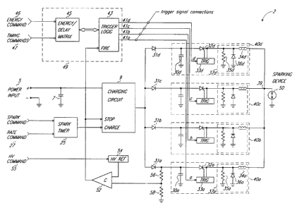
FIG. 9 is a schematic diagram of another
alternative embodiment of the invention adapted for use as
a high-rate, multi-output ignition system.
FIG. 10a is a schematic diagram of the preferred _
charging circuit.
FIG. IOb is a schematic diagram of an
alternative charging circuit.
FIG. lOc is a schematic of another alternative
charging circuit which, among other things, isolates the
energy storage devices of the output stages from one
another.
newc~r9otioa of the Preferred Embodiments
FIG. 1 shows generally a block diagram
representation of a circuit 2 for controllably generating .
sparks constructed in accordance with the teachings of the
instant invention. By varying certain input parameters as
discussed below, a user can cause this circuit 2 to
generate sparks having virtually any energy level and
plume shape (i.e., energy distribution, three-dimensional
shape, spatial intensity, and duration; any or all as a
function of time, if desired). Thus, the circuit 2 is
particularly well suited for use in a piece of teat
equipment which could be employed to determine the optimum
plume shape and energy level of sparks generated for a
particular application. To thin end, the circuit 2
includes a spark generating device 50 for creating a
spark; a plurality of. independently triggerable output
stages 40a, 40b, 40c, 40d connected to the spark
generating device 50 for storing and selectively
transferring energy thereto; and a logic circuit 49 for
selectively firing one or more of the output stages 40a,
40b, 40c, 40d to create a spark of a desired plume shape
and energy level at the spark generating device 50.
The spark generating device 50 can be
implemented by a variety of devices, but it typically
includes a set of electrodes between which a plasma forms
,~ ~18~~~~
- page 11 -
for conducting electric current when a sufficiently high
potential difference is placed across the electrodes. The
spark generating device 50 can be an igniter plug or spark
plug suited for the application for which a spark is being
S generated. In addition, the spark generating device 50
can be an assembly in which existing structural parts are w
used as the spark electrodes, such as in the nozzle
assembly of a spacecraft thruster, or a spark rod tsingle
electrode) in an industrial burner where the burner itself
serves as the other-electrode. Indeed, the possible
implementations of the spark generating device are as
varied as the multitude of applications for which this
. invention provides beneficial performance. Such
applications include ignition of: all types of engines,
- -_._. .
turbines, burners, boilers, heaters, arc-lamps, strobe
lamps, flarestacks, incinerators, pyrotechnic detonators,
cannons, rockets, and thrusters.
Turning first to the application of power to the
circuit 2; the embodiment of the invention shown in FIG. 1
includes a power input 5 which receives the electrical
energy used by the output stages 40a, 40b, 40c, 40d from
an external power source. The power input 5 can be used
in conjunction with any source of DC power including
batteries and other conventional power supplies known in
the art, including rectified AC power (i.e., 120 Vac, 60
Hz. commercial power)'. Optionally, the power may be
conditioned by an EMI (ElectroMagnetic Interference)
filter (not shown) or.other filtering devices if desired.
Once received, the power is preferably stored locally in a
capacitor-7 before it is used by a charging circuit 9.
The general purpose of the charging circuit 9 is
to provide control over the charging cycles of circuit 2.
In order to provide this control, the charging circuit 9
includes inputs 20, 22 for receiving two signals
designated CHARGE and STOP. As their names suggest, the
arrival of a CHARGE signal at input 20 causes charging
circuit 9 to begin a charging cycle by providing energy in
~~8~.f~~2
- page 12 -
the form of an output voltage or pulses to the energy
storage devices_ On the other hand, the arrival of a STOP
signal at input 22 causes the charging circuit 9 to
terminate the charging cycle by ceasing its output.
In the preferred embodiment, the charging
circuit 9 is implemented by a flyback converter such as
that shown in FIG. 10a. However, those skilled in the art
will appreciate that any type of charging circuit capable
of producing a high voltage (for example, 500 to 5000
volts) or a series of high voltage pulses would also be
acceptable in this role. As shown in FIG. 10a, the
preferred charging circuit 109 includes a control circuit
110 which modulates a switching device 112 such as a
MOSFET to chop the current flow through the primary _
winding 114 of a transformer. The chopping is usually
done at a high frequency (for example, 10 to 100
kiloherta) to permit the use of a transformer of
relatively small physical sine. The current in the
primary winding 114 is preferably monitored by a current
sensing device such as current sensing resistor 118. The
voltage across the current sensing device 118 provides the
control circuit 110 with a feedback signal which is used
in the modulation of the switching device 112. Each time
the current in the primary winding 114 is interrupted
(chopped), energy is transferred to the secondary winding
I16 of the transformer where it emerges as a high voltage
pulse in a manner known in the art. Although so called
DC-to-DC converters often include a rectifier stage and an
' output storage capacitor or other filtering circuitry to
smooth the pulses into a steady DC level, such a stage
would be redundant in this embodiment since the succeeding
stages perform.this smoothing function as explained below.
As illustrated in FIG. 10a, the control circuit
110 includes two inputs 120, 122 for the CHARGE and STOP
signals. The arrival of a CHARGE signal at input 120
causes the control circuit 110 to begin a charging cycle
by commencing the modulation of switch 112 to thereby
CA 02181092 2005-03-07
- page 13 -
produce charging pulses in the secondary winding 116. This
activity continues until a STOP signal is received at
input 122. When such a signal is received, the control
circuit 110 terminates the charging cycle by ceasing the
modulation of switch 112 thereby stopping the generation
of the charging pulses.
In certain systems which have appropriate high
voltages) available, the high voltages) may be applied
to the power input 105 and used without any voltage
conversion as shown in FIG. lOb. In this simpler charging
circuit 119, the CHARGE 120 and STOP 122 inputs cause a
switching device 115 to toggle between it conducting and
non-conducting states. When in its conducting state, the
switching device 125 transmits energy from power input 105
to a plurality of isolating diodes I3Ia, 131b, 131c, 131d
which are connected to the output of charging circuit 119.
When deactivated, the switching device 115 blocks
transmission of energy from the power input 105, thus
ceasing the charging of the energy storage devices via the
diodes 131a, I3lb, 131c, 131d.
Referring again to FIG. 1, the CHARGE signal is
generated periodically by a spark timer 25 at a repetition
rate equal to the desired sparks-per-second rate. This
rate may be adjustable in which case a-rate command 27
input by a user would establish the setpoint, or it may be
fixed by the circuit values depending on the intended use
of the device. In another alternative implementation, the
spark timer '25 is provided with a rate command 27 which
automatically changes from a higher to a lower rate at a
certain time after sparking first commences. This
burst-of-sparks mode is fully described in U.S. Patent
5,399,942,
Preferably, the spark timer 25 includes an input
for receiving a spark command 29 which, together with the
rate command 27, provides several possible operating
modes. In a first mode, the spark command 27 is
2.~8~.09~
- page 14 -
synonymous with the application of power so that sparking
commences immediately when the power input 5 receives
power, and ceases when that power is removed. In a second
mode, the spark command 29 is an external input as shown
in FIG. 1 which permits an operator of the apparatus to
decide when to commence or cease sparking while the power-
at power input 5 is maintained. In a third mode, the rate
command 27 is set to a repetition rate of zero so that
each individual spark command 29 causes a single spark.
Upon receiving a CHARGE signal the charging
circuit 9 provides a charging voltage which is transmitted
via isolating diodes 31a,'31b, 31c, 31d to the inputs of
_ the plurality of output stages 40a, 40b, 40c, 40d. These
output stages 40a, 40b, 40c, 40d are substantially _
structurally identical in this embodiment. They each
include: an energy storage device 30a, 30b, 30c, 30d; a
controlled, switch 32a, 32b, 32c, 32d with an associated
triggering circuit 33a, 33b, 33c, 33d; and a network 37a,
37b, 37c, 37d. In view of these similarities, and in the
interest of simplicity, the following discussion will use
a reference numeral in brackets without a letter to
designate an entire group of substantially identical
structures. For example, the reference numeral [30] will
be used when generically referring to capacitors 30a, 30b,
30c and 30d rather than reciting all four reference
numerals.
It should be noted that, although for simplicity
the output stages (401_have been described as
substantially identical in this embodiment, as explained
in further detail below, the capacitance values) of one
or more of the individual energy storage devices [30], as
well as the voltages) these devices [30] are charged to,
can be varied from one another to permit the circuit 2 to
produce sparks having a greater range of plume shapes
and/or energy levels without departing from the scope or
the spirit of the invention. Indeed, in many
applications, employing capacitors having different
~18I~92
- page 15 -
capacitance values as the energy storage devices [40] is
preferred. Several approaches to selecting these
capacitance values are described in detail below.
As shown in FIG. 1, the storage capacitors [30]
are charged by energy emanating from the output of the
charging circuit 9 via the isolating diodes [31]. These
diodes [31] perform three distinct functions. First, when
necessary, they rectify the pulsed output of certain
converters such as the flyback converter shown in FIG. 10a
to provide pulses of only one polarity so that each
successive pulse incrementally charges the capacitors
[30]. Second, the diodes [31] prevent the energy stored
in the capacitors [30] from leaking back through the
charging circuit 9. Finally, the diodes (31] isolate the _
capacitors [30] from one another. Without the diodes
(31], the capacitors [30] would be in parallel
electrically and would, therefore, represent the
equivalent of a single larger capacitance having a value
equal to the sum of the individual parallel capacitances.
In such a case, discharging one of these parallel
capacitors would have the effect of discharging them all.
In the preferred embodiment, however, the multiple diodes
[31] allow all of the capacitors [30] to be charged from
the same charging circuit 9, and further permit each of -
the capacitors [30] to be discharged individually via the
controlled switches [32] without affecting the charge of
the others. Thus, if only a particular switch (such as
32a) discharges its associated capacitor (i.e., 30a) the
remaining capacitors (i.e., 30b, 30c, 30d) will remain
charged; ideally until such time that their respective
switches (i.e., 32b, 32c & 32d) are triggered.
Although the direction (polarity) of the diodes
[31] produces a positive charge on the capacitors (30], it
will be appreciated by those skilled in the art that the
polarity of the diodes [31], the switches [32], and the
other associated components can be reversed to produce a
negative charge and correspondingly negative output pulse
~18i~9~
- page 16 -
without departing from the scope or the spirit of the
invention.
The controlled switches [32] are preferably
silicon controlled rectifiers (commonly referred to as
SCR s or thyristors). However, it will be appreciated by
those skilled in the art that other controlled switching
devices which are capable of operating at the voltage and
current levels generally associated with spark generating
may be substituted for the SCR devices without departing
from the scope or the spirit of the invention. In this
regard, it should be noted that the switching device does
not need to be a solid-state (semiconductor) device.
Instead, it need only be triggerable by the control
circuits. Thus, certain other triggerable spark-gap
switches, other types of semiconductor devices such as
MOSFETs or MCTs (Mos Controlled Thyristors), and
electromechanical switches such as relays can all be
appropriately employed as the controlled switches [32]
without departing from the scope of the invention. It
should also be noted that, although an exemplary
triggering circuit and technique is described below, other
triggering methods employing electrical, optical,
magnetic, or other signals appropriate to the device
chosen for the controlled switch can be used in this role
without departing from the scope or the spirit of the
invention.
In the alternative embodiment illustrated in
FIG. 2, a plurality of_charging circuits [209] similar to
charging circuit 9 is used to charge the capacitors [230]
of the output stages [240] independently of one another.
This alternative approach offers several advantages over
the single charging circuit embodiment shown in FIG. 1.
For example, it permits the circuit to generate a greater
range of output waveforms having a greater range of total
energy levels and waveshapes. More specifically, the use
of separate charging circuits enables each capacitor [230]
to be charged to a different voltage such that each output
~18~~~2
- page I7 -
stage (240] has a different level of stored energy.
Consequently, each stage will transfer a particular amount
of energy (i.e., dependent on both its stored voltage and
its capacitance) to the spark generating device 50 when
fired. A user can then elect to fire one or more of the
stages [240] in combination to arrive at a desired output.
Another advantage of this approach is that, instead of
taxing a single charging circuit, the work associated with
charging the capacitors is divided among a plurality of
charging circuits [209]. Such an approach results in
greater power throughput than can typically be achieved
using a single charging circuit (unless simple charging
circuits similar to that illustrated in FIG. lOb are
employed as the plurality of charging circuits). _
Finally, this approach permits the exclusion of
the isolating diodes [31] since the separate charging
circuits serve as a means for charging the energy storage
devices and at least partially isolating each of the
energy storage devices from the energy storage devices in -
the other output stages.. In the single charging circuit
embodiments, the charging circuit and the isolating diodes
combine to form a means for charging the energy storage
devices and at least partially isolating each of the
energy storage elements from the energy storage elements
of the other output stages.
Although the embodiment of FIG. 2 assigns one
charging circuit to every capacitor, those skilled in the
art will appreciate that any other combination of charging ---
circuits and capacitors can be used without departing from
the scope or the spirit of the invention. For example,
one could divide the stages [240] into groups of two and
assign each group a single charging circuit without
departing from the invention: In addition, those skilled
in the art will appreciate that the charging circuits can
be configured to produce either different output voltages
or identical output voltages without departing from the
scope or the spirit of the invention.
CA 02181092 2005-03-07
page 18 -
Some of the benefits of employing separate
charging circuits as shown in FIG. 2 can be realized by
employing the less complex charging circuit 129 shown in
FIG. lOc. In this circuit multiple secondary windings.
[116] on the converter transformer_separately provide
isolated charging pulses to the output stages. Because
the windings [116] are separate, they can be constructed
to generate the same or different charging voltages. The
rectifier diodes [131] in FIG. lOc, although located in a
similar position as the isolating diodes in other figures,
are used principally as rectifiers of the AC output pulses
characteristic of converter circuits, since the isolation.
function is accomplished by the separate windings [116].
It will be appreciated by one skilled in the art that the
multiple windings [116] could comprise a single winding
with multiple taps, thus providing the different voltages.
However, in such an approach, the windings would not
isolate the output stages from one another and the
isolating diodes would, therefore, be needed in this
isolation role.
Returning to the embodiment illustrated in FIG.
I, the description of any one of the plurality of output
stages [40] included in this embodiment will serve for ail
since, as explained above, these stages [40] are
substantially structurally identical. Specifically, each
of the output stages ~ [40] includes : an energy storage
element [30], a controlled switch [32], and an output
network [37]. The operation of such a circuit is
described in detail in U.S. Patent 5,245,252
Thus, the construction and operation of the circuits [40]
will only be described briefly here. The interested reader
is referred to the '252 Patent for a more detailed
description.
As mentioned above, the energy storage elements
[30], which are preferably capacitors, are charged by the
charging circuit 9 via isolating diodes [31]. At any time
z~s~o~z
- page 19 -
after the capacitors [30] have reached their prescribed
levels of charge, the logic circuit 49 can selectively
discharge any of these devices by triggering the
appropriate controlled switch [32]. To this end, the
trigger logic 43 is coupled to the output stages [40] via
four separate trigger signal connections [41]. It will be
understood that four separate connections [41I are
preferably employed, although a single communication line
with appropriate multiplexing circuitry could be employed
in this capacity if desired, as could indirect coupling
(for example, the use of fiber-optic links), without
departing from the scope or the spirit of the invention.
In any event, the trigger signal connections
[41] couple the trigger logic 43 to a trigger circuit [33] .
in each of the output stages [40]. These trigger circuits
(33] are each equipped to open and close their associated
controlled switch [32] in response to a trigger signal
from the trigger logic 43.
The trigger circuits [33] may contain a variety
of circuitry depending on the specific component used to
implement the controlled switches [32]. Preferably, they
include isolation components which protect the
lower-voltage logic circuits 49 from the higher voltages
present at the switches (32]. in the preferred
embodiment, which uses SCR's as the controlled switches
[32], a pulse (trigger) transformer with associated drive
circuitry known in the art is employed as the trigger
circuit [33]. The secondary winding of this transformer
is connected to the gate and cathode terminals of its
assigned SCR, and its primary winding is connected to the
trigger signal connection [41]. The trigger logic 43 can
then energize the transformer via a control signal which
induces a current in the secondary winding of the
transformer that is sufficient to transition the SCR to a
conducting state.
When activated in this manner, the controlled
switch (32] transitions from its off (non-conducting)
~~8~t1~2
- page 20 -
state to its on (conducting) state. This allows the
energy stored in capacitor [30] to flow through the
network (37] to the output of circuit [40] where it is
delivered to a sparking device 50 to create an ignition
spark. Since the outputs of all of the output stages [40]
are connected to the sparking device 50 via junction 39,
the energy delivered to the sparking device 50 will be the
overlapping, partially overlapping, or non-overlapping
summation of the energies delivered by each triggered
output circuit I40] depending on the timing of their
firing.
It should be noted that, although for clarity
only a single device has been shown to represent the
controlled switch, as taught in the previously referenced
'252 patent, the controlled switch [32] may comprise a
group of devices triggered simultaneously as if they were
a single device without departing from the scope or the
spirit of the invention.
Each network (37] in the preferred embodiment
consists of three components: an inductance [34]
(preferably a saturable core inductor as disclosed in the -
'252 Patent) connected so that the current must pass
through it on its way to, or-from, the sparking device 50;
a resistor [35]; and an optional unipolarity diode [36]
connected to ensure a nominally unidirectional discharge
current to the spark~generating device 50 if a unipolar
ignition is desired. The networks (37] of the output
stages (401 perform several important functions. First,
they waveshape the voltage and current of the output
waveforms to improve ignition. Second, they provide
protection for the solid-state switch [32] in the circuit
by holding off the current discharged from the capacitor
I30] for a time sufficient for the switch [32] to
transition from its non-conducting state to its conducting
state. These functions are described in detail in B.S.
Patent 5,245,252 and will not be described in further -
detail here.
. ~181~~J~
- page 21 -
In the instant invention, the networks (37] have
a third purpose. Specifically, since all of the networks
(37] are connected to the spark generating device 50 via
junction 39, the networks [37] must also provide a degree _ .
of reverse isolation so that the discharge of one stage
does not inadvertently false-trigger any of the other
stages. Whenever one or more of the output stages (40] is
discharged, the junction 39 where. all of the stages [40]
connect together with the sparking device 50 is subjected
to large voltage transients. For example, when one of the
switches [32] is closed, the junction 39 is driven to the
voltage previously stored in the tank capacitor [30].
_ Then, at the instant the spark plasma forms with its
extremely low resistance, the junction 39 is driven back
toward ground (zero volts). This transient pulse would .
impress a large dv/dt stress on the untriggered switches
[32] if the network [37] were not present to isolate the
switches [32] from the junction 39. With the network (37]
in place,-the values of the inductance [34] and resistance
I35] can be chosen to act as a low-pass filter, thus
preventing the high dv/dt transient pulse at the node 39 ..
from reaching the untriggered switches [32].
Those skilled in the art will appreciate that
the inductor [34] may be located elsewhere (for example,
in the ground return path) so long as the discharge
current passes through it as well as through the spark
generating device 50.
Those skilled.in the art will further appreciate
that many arrangements of output networks which produce a
similar isolating result could be employed'without
departing from the scope or the spirit of the invention.
For example, in the alternative embodiment illustrated in
FIG. 3, the networks [337] each include a diode [300]
which permits energy to flow from any stage [3403 through
the junction 339 and to the sparking device 350. However,
the diodes [300] also prevent reverse energy from
transferring back from the junction 339 into the output
~~.8~~92
- page- 22 -
stages [340]. The use of diodes [300] to isolate the
outputs of the stages [340] is similar conceptually to the
use of diodes [31] to isolate the inputs of the stages
[40] that was described earlier with reference to FIG. 1.
There is, however, an important difference between the two
implementations. Specifically, the magnitude of the
current carried by the diodes [31], (331] at the inputs of
the discharge stages (40], [340] is relatively small
compared to the currents carried by the output diodes
l0 1300]. For instance, the output currents are typically on
the order of several hundred to.thousands of Amperes
whereas the input currents are usually on the order of
. tens to hundreds of milliAmperes. Electrical losses in ar_
imperfect diode are proportional to the current it pasaes_ .
Therefore, while the diodes 7300] incorporated into the
output networks [337] of the device would provide good
reverse isolation, they are inefficient when used to carry
current of large magnitude and would rob part of the
discharge-energy. Also,,inclusion of a diode in the
manner illustrated by FIG. 3 restricts the circuit to
unipolar operation. As a result of these limitations,
this isolation technique is not preferred.
In the embodiment shown in FIG. 3, the diodes
[300], as shown, are all connected to junction 339_
However, as those skilled in the art will appreciate, the
networks (337] could be modified to perform substantially
the same function by reversing the positions of each
inductor [336] and its-series-connected diode [300]
without departing from the scope or the spirit of the
invention.
Certain ignition applications may require
modifications to the embodiment shown in FIG. 1. For
example, if a bipolar ignition is desired, the networks
[437] of the output stages [440] could be modified as
shown in FIG. 4. It should be noted that although for
simplicity FIG. 4 only illustrates one of the output
stages 440a in detail, the other output stages 440b, 440c
~~siasz
- page 23 -
would be similarly constructed. In addition, it should be
noted that FIG. 4 illustrates an embodiment of the
invention having only three output stages [440]. However,
like all of the other embodiments of the invention, it
could be constructed with any other multiple number of
stages (i.e., at least two) without departing from the
scope or the spirit of the invention.
The bipolar circuit 402 illustrated in FIG. 4
does not include the unipolarity diode (36] that was used
i0 in the unipolar circuit of FIG. 1 because in bipolar
ignition systems the, current through the spark generating
device 450 reverses direction for a substantial portion of
the energy delivezy cycle. In both the bipolar and
unipolar systems, the current transfers the energy in the
capacitor [430] to the spark generating device 450 via the
inductor [434]. However, not all of the energy is
dissipated in the first portion of the discharge cycle.
Some of the energy remains in the inductor [434]. In a
unipolar circuit such as that shown in FIG, 1, this energy
would ultimately be discharged from the inductor [34] in a
later part of the discharge cycle via the freewheeling
diode [36] with the current discharging in the same
direction through the spark generating device 50
throughout the cycle. In bipolar circuits such as that
shown in FZG. 4, the second part of the cycle is
characterized by a reversal of the current flow by which a
portion of the energy in the inductor (434] is transferred _
back to the capacitor.[4~0] with most of the remaining
energy being consumed by the spark generating device 450.
The residual, unconsumed energy continues to oscillate
back and forth between the inductor (434] and the
capacitor [430] with each surge supplying additional
energy to the spark plasma until the energy is dissipated.
Such oscillations should not be confused with
short duration oscillatory transients which are typically
present in circuits. Although such "noise" transients
appear to have high magnitude, they do not transfer
- page 24 -
significant useful energy to the plasma. Noise transients
such as these appear in many circuits including circuits
designed to be substantially unipolar. Although these
transient noise pulses may be bipolar, the circuit is
still a ~~unipolar circuit" as long as the main energy
transfer is a substantially unipolar event.
An anti polarity diode (401] is a necessary part
of the network [43'7] when certain semiconductor switching
devices L432] are used. Such a diode [4011 permits the
reversed current to flow, but bypasses the switch [432] so
that the switch, is not damaged by a reverse current flow
through it. In these embodiments, the trigger circuit
[433] must ensure that the controlled switch [432] remains
conductive throughout the several cycles which include
reversals of current.
In high-tension ignition embodiments, the spark
generating device has a breakdown voltage (the minimum
voltage for the plasma to form) which is generally beyond
the practical limits of the switching device, capacitor,
and other components of the individual output stages [40].
To overcome this difficulty, these systems may employ a
special inductor/transformer 599 in one or more of the
networks of their output stages as shown in FIG. 5a. A
first winding of this device 599 is preferably connected
in series arrangement (end-to-end, in any order) with the
capacitor 530, switch 532, and spark generating device 550
in a similar position as the inductor [34] of FIG. 1. A
second winding of the.inductor/transformer 599 is
magnetically coupled to the first winding for transferring _
a voltage pulse thereto when the controlled switch 532 is
triggered. -Thus, when the switch 532 is triggered, a
transient pulse across the second winding creates a
voltage across the first winding which is additive with
the voltage already impressed upon that first winding by
the closure of the switch 532. Although the exact value
of this voltage depends on the turns-ratio of the first
and second windings, their combined voltage can have a
~18~~9~
- page 25 -
magnitude of several to tens of times greater than the
energy storage voltage provided by the capacitor 530
alone. While the additive effect of the pulse through the
secondary winding is generally of a short duration
relative to the overall discharge event, (a limiting
device 508, which is preferably a small capacitor, is
usually employed in series with the second winding to
limit the pulse to a short transient which consumes only a
small percentage of the energy that was stored in
capacitor 530), the increased voltage at the initiation of
the discharge event is sufficient to create a plasma in a
high-tension spark generating device 550. After this
. plasma is formed, the resistance between the electrodes
becomes negligible and the main discharge current then _
flows through the series-connected first winding which
acts in the same manner as the series output inductor
described above in connection with FIG. 1 without further
assistance from the second winding.
'Those skilled in the art will appreciate that
the exact placement and polarity of the connections of the
inductor/transformer 599 is not critical so long as the
additive effect creates an ionizing pulse of sufficient
positive or negative polarity to cause the plasma to form
at the high-tension spark generating device 550.
Furthermore, like the ionization pulse, the
post-ionization discharge current {i.e., the current
following the initial ionizing pulse) may be either
bipolar or substantiall.~ unipolar. In the case of a
substantially unipolar post-ionization discharge current,
the circuit is referred to as a "unipolar circuit~~, and
the presence of a bipolar ionizing pulse or an ionizing
pulse having a polarity opposite to that of the
post-ionization discharge current does not change this
definition. In other Words, for purposes of this
application, a circuit is defined to be unipolar even if
the polarity of the current discharging through the spark
generating device is opposite to the polarity of the
~18~092
- page 25 -
ionization pulse and/or even if the ionization pulse
itself is bipolar as long as the post-ionization discharge
current flows substantially in one direction.
In a related embodiment illustrated in FIG. 5b,
the current through the second winding of the
inductor/transformer 599 is driven and controlled by one
of the other output stages 540b. The inductor/transformer
599 thus serves to combine the energies discharged by the
two stages 540a/540b into a common output. As will be
appreciated by those skilled in the art, the inductors
[534] of the other stages [540] can be combined into the
output by connecting ti:em to ju.-~ction 539 or,
. alternatively, they car_ be added to the
inductor/transformer 599 as add_tional windings in order
to combine the energies of these additional stages with
the stages illustrated in FIG. ~b without departing from
the scope or the spirit of the _avention.
In another re'_ated esbodiment illustrated in
FIG. Sc, the high-tens_on inductor/transformer 599 is a
separate device (not replacing any inductor [534]) which
is connected so that lea-tension pulses at junction 539
will have a transient high-tens_on ionizing pulse added to
them for the purpose of ionizing the gap of the spark
generating device 550 to create a plasma.
The embodiments shown in FIGS. 5a, 5b, and 5c
are configured as unipolar circuits. Alternatively, these
embodiments could be ccnfigured as bipolar circuits, for
example, by modifying tae circuits as taught above in
reference to FIG. 4.
Generally, the plurality of stages may be
configured to have any combination of constructions. For
example, one stage could be configured as a bipolar
circuit while a different stage could be configured as
substantially unipolar. Similarly, another stage could be
configured as high-tension and yet another configured as
low-tension. All of these stages acting together produce
the ultimate waveshape which reaches the spark generating
218 (l92
- page 27 - -
device. Furthermore, the controlled relative timing of
the discharges in circuits combining these techniques
(i_e., bipolar, unipolar, high-tension, and low-tension
pulse generation) in any combination adds yet another
degree of complexity to the waveshape of the pulse
supplied to the spark generating device and, thus, to the
time-varying plume shape of the sparks generated.
Turning again to FIG. _, the output circuits
(40] are, in large part, control_ed by two main elements:
a voltage sensing comparator 52 and the logic circuit 49.
These elements 52, 49 combine wi~h the above mentioned
spark timer 25 to achieve total control of the spark
. generation. More specifical'_y, after the spark timer 25
requests the next spark event by activating the charging _
circuit 9, the comparator 52 begins to continuously
monitor a signal taken from a vo_tage divider network
consisting of resistors 56 and 5d. This signal is
proportional to the voltage appearing across the energy
storage capacitors (30].. The comparator 52 compares this
proportional signal with a reference voltage received from
the I3V reference 54 to determine when the capacitors [30]
have reached a predetermined voltage.
Although in the embodiment illustrated in FIG.
1, a voltage divider and voltage-sensing comparator is
employed to monitor the voltage of the capacitors [30],
those skilled in the art will appreciate that other
structures for indirectly or directly monitoring the
voltage across the capacitors [30] such as structures
which measure the charge time in a circuit that charges
the capacitors 1307 at a constant rate could be employed
without departing from the scope or the spirit of the
invention.
When the capacitors [30] reach their desired
charge, the voltage produced by the voltage divider will
equal the voltage appearing at the HV reference 54. At
that instant, the comparator 52 will switch its output to
signal the event to the other circuit blocks. One
- page 28 -
destination of tae signal generated by the comparator 52
is the STOP input 22 of the charging circuit 9. When the
charging circuit 9 receives this signal, it stops charging
the capacitors [30]. Thus, the energy stored by the
capacitors [30] a closely controlled. In the embodiment
illustrated in F-G. 1, an input 55 allows the operator to
input a HV command tc preset the exact charge voltage of
the capacitors [303. In some production apparatus, this
input 55 may be emitted and the voltage.value fixed so
that all sparks are delivered at the same optimum voltage
without the user's involvement.
In the embcdiment illustrated in FIG. 1, the
above described voltage control is accomplished by
monitoring only cne c. t:.e plurality of output stages [40]
since alI of the capacitors (303 are charged to the same
voltage. When capacitors of varying sizes are employed,
it has proven ad-rantageous to monitor the smallest of the. .
capacitors [30] because its voltage changes more rapidly
than the voltages of the ether capacitors (i.e., it has
~0 the fastest electrical time constant). Many more
complicated circuits can .~-,e constructed to monitor more
than one of the output stages. For example, it may be
useful to select the 'uighest of a plurality of monitored
voltages for use as the feedback signal.
In other embodiments such as that shown in FIG.
2, a plurality o. charging circuits [209] is employed;
with each such c~arging circuit [209] having an assigned
storage capacitor [230]._In this embodiment, a voltage
sensing network a provide3 in each stage [240] to permit
each charging circuit I2097 to separately monitor the
charging of its assigned capacitor [230]. Each charging
circuit [209] in FIG. 2 includes a comparator (not shown)
similar to the comparator 52 illustrated in FIG. 1 or
other equivalent circuitry which stops the charging
(similar to the STOP signal 22 of FIG. 1) and provides an
individual FIRE signal 244a, 244b, 244c, 244d to the
trigger logic 243.
~
2~8~f~~~
- page 29 -
The single point monitoring illustrated in FIG.
1 is advantageous only from a circuit simplicity and
expense standpoint, and can only be used in embodiments
where all of the capacitors [30) are charged to the same
voltage.
The second destination of the signal generated
by comparator 52 is the logic circuit 49. As shown in
FIG_ 1, this signal is received at the FIRE input 44 of
the trigger logic 43 which tells the circuit that the
desired energy storage level has been accomplished and
that the output stages (40) are, thus, ready for firing.
In the preferred embodiment, the trigger logic 43 triggers
the stages [40] by sending trigger signals down the
appropriate trigger signal connections [41) in accordance
with rules stored in the energy/delay matrix 45. These
rules determine whether each individual stage is fired at
all, and when, relative to the firing of the first stage,
they will each be fired. Thus, depending on the rules
stored in the energy/delay matrix 45, the trigger logic 43
will trigger one or more~of the output stages [40] to
transfer an overlapping, partially-overlapping, or
non-overlapping output waveshape or pulse to the spark
generating device 50. The spark generating device 50 will
then produce a spark whose time-varying plume shape and
energy level will correlate to the waveshape and energy
level of the received pulse.
it should be noted that, for purposes of this
patent application, "plume shape" refers to a single
charging/discharging cycle. Thus, if the apparatus is
configured to produce a sequence of two or more sparks
within a single charging/discharging cycle, it still
produces a single plume shape for that cycle (i.e., a
plume shape with at least one instant of zero energy
between the inception and termination of ionization at the
spark generating device during a given
charging/discharging cycle). Of course, it also produces
a single plume shape if it produces a single spark during
- page 30 -
a given charging/discharging cycle (i.e., with no instants
of zero energy between the initiation and termination of
ionization at the spark generating device during a given
charging/discharging cycle).
The energy/delay matrix 45 may be preset, or it
may receive either or both an ENERGY command 46 and a
TIMING command 47 from an operator of the apparatus. The
ENERGY command 46 controls the total energy which will be
transferred to the spark generating device 50 by
determining which of the stages [40] will be fired in
combination to produce the requisite summation equaling
the desired total energy. The energy/delay matrix 45 can
. be configured in the form of a look-up table. Thus, for -
any energy level a user might request, the energy/delay .
matrix 45 would have a corresponding setpoint that
indicates which stages (40] should be fired to achieve the
desired result. The energy/delay matrix 45 could also be
used to store data indicating the voltages) the stages -
[40], (140] should be charged to. Of course, the
energy/delay matrix 45 can be so configured in any
embodiment of the invention.
Finally, after all selected output stages have
been triggered, the circuit rests before the spark timer
initiates the next cycle. The interval between spark
25 cycles, which commences upon the completion of the
discharge of the slowest-discharging stage, must be long
enough to permit the controlled switches [32] to
transition fully to thea.r non-conductive states before the
next charging cycle begins.
In the preferred embodiment, the capacitance
values of the energy storage devices [30] of the output
stages [40] are binary weighted to permit the device to
generate pulses having a wide range of output energies.
(Those skilled in the art will, however, appreciate that
this same weighting effect could be achieved by using
identical capacitors charged to different voltages in
accordance with the above-described techniques.? Thus,
~.~8Ia9~
- page-31 -
the stages [40] are given the relative energy scaling
1:2:4.8. In other words, if the smallest of the stages
has an energy of 1 (one) unit, then the other stages have
2 (two) units, 4 (four) unite, and 8 (eight) units of
energy, respectively. This weighting permits the device -
to generate a pulse having any energy level between 0 and
units (16 distinct levels) by firing various
combinations of the stages [40]. For example, firing only
the 1 unit and 4 unit stages produces the sum: 1 + 4 = 5
10 units. It should be noted that the scaling unit is not
necessarily 1 Joule. Instead, the scaling system is
equally useful regardless of the base unit chosen. For
_ example, if-the base unit has a value of 1/2 Joule, then
firing the above combination of stages (40] would produce _
15 an output pulse having:
1/2 * ( I + 4 ) = 2.5 Joules
of total energy. Thus, the energy of the pulse generated
by the apparatus equals the base unit multiplied by the
collective sum of the scaling factors of the stages fired.
The maximum energy of this four stage embodiment is then:
UNIT VALUE * ( 1 + 2 + 4 + 8 ) = UNIT VALUE * 15
In actual practice, there may be other
limitations which necessitate deviation from the optimal
binary weighting of the stages. In one implementation of -
the invention that has been tested, the smallest stage was
designed to store and fire 1.0 Joule of energy. In
combination with two other stages designed to fire 2.0 and
4.0 Joules of energy,.respectively, an apparatus was
constructed which generated pulses having up to ( 1.0 +
2.0 + 4.0 ) = 7.0 Joules of total energy. In order to
produce a higher maximum output a fourth stage was needed,
but following the binary weighting rule would require a
single stage capable of generating 8.0 Joules of energy.
This level of energy was beyond the practical limitations
of the exact components which had been used to construct
the other three stages. Thus, a capacitor capable of
storing 5.0 Joules of energy was selected for the fourth
~~81t~92
- page 32 -
stage and the final device generated sparks having a
maximum total energy of:
1.0 * ( 1 + 2 + 4 + 5 ) = 12.0 Joules
while this is a useful result, it is not optimal
because this system could only produce pulses having 13
distinct energy levels ( 0 through 12 ) whereas a true
binary weighting system could produce pulses having 16
distinct levels of energy. The loss of 3 possible energy
levels is due to redundancies in the sequence.
Specifically, three energy levels can be achieved by
firing either of two different combinations of stages that
sum to the same total value:
_ level 5 .is either ( 5 ) or ( 1 + 4 )
level 6 is either ( 1 + 5 ) or ( 2 + 4 )
13 level 7 is either ( 1 + 2 + 4 ) or ( 2 + 5 )
Thus, while there are still 16 possible combinations, only
13 of those combinations produce distinct energy levels.
Those skilled in the art will recognize that the above
exemplary device could be modified to perform in
accordance with a true binary weighting system by
replacing the five Joule stage with two 4.0 Joule
sub-stages which are fired simultaneously to discharge 8.0
Joules of energy.
The other input to the energy/delay matrix 45 is
the TIMING command input 47. This command controls the
timing and order for triggering the various output stages
j40]. The timing sequence begins anew each time the FIRE
input 44 of the trigger_a.ogic 43 receives a signal from
the comparator 52. In the preferred embodiment, the
trigger logic 43 relies on data stored in the energy/delay
matrix 45 to generate each of the plurality of trigger w--
signals after a delay specific to the corresponding stage
stored in the matrix 45 has passed. The actual generation
of the trigger signal occurs if, and only if, that stage
is active according to the ENERGY command that was last
stored in the matrix 45.
~~c~~~~~
- page 33 -
In the embodiment shown in FIG. 1, the TIMING
commands may be thought of as four separate delay commands
corresponding to the four individual stages [40] shown in
the figure. If the number of stages is less or more than
four, then the number of delay commands corresponds to
that number of stages. In certain production apparatus
there may not be a delay function, in which case the
trigger logic 43 delivers trigger signals simultaneously
to whichever stages are to be fired.
The magnitude of the delay for any stage [40]
ranges from zero to a practical maximum which is
determined by the self-discharge time of the apparatus of
FIG. 1. At the same instant that the trigger logic 43
receives the FIRE signal, the charging circuit 9 receives -
its STOP signal and ceases charging the capacitors [30].
In the preferred embodiment, any stage which is not
triggered at this time begins a relatively slow
self-discharge of its stored energy due primarily to
leakage through the lesssthan-perfect controlled switch
[32] and resistor [35]. After some amount of time
determined by the component values, the capacitor [30]
loses its useful energy, and a trigger signal occurring
after that time would have little effect.
In the preferred embodiment illustrated in FIG.
6, the logic circuit 649 is implemented by a
microprocessor 600. The microprocessor 600 is used to
perform many of the logic functions described in
connection with the embodiment shown in FIG. 1. In the
microprocessor embodiment shown in FIG. 6, the
microprocessor 600 performs the functions of the following
elements of the FIG. 1 embodiment. the spark timer 25,
trigger logic 43, the energy/delay matrix 45, the
comparator 52, and HV referehce 54. Depeading upon the
type of microprocessor employed, if the preferred -
charging circuit illustrated in FIG. IOa is used the
microprocessor 600 may be optionally configured to perform
the functions of the control circuit 110. It will be
CA 02181092 2005-03-07
- page 34 -
appreciated that the microprocessor 600 can also be
configured to perform similar control functions with other
charging circuits without departing from the scope or the
spirit of the invention.
As shown in FIG. 6, the microprocessor 600 is
provided with a data I/O port 630 which serves as a
communications link between the microprocessor and an
operator interface. This interface is most'likely another
computer or terminal with a keyboard input and display
capabilities which allow an operator to program the
apparatus via the data I/0 port 630. Two alternative
interfaces have been implemented and can be used
interchangeably: a personal computer connected to the
data I/O port 630 via the computer's SERIAL COM PORT, and
I5 a dedicated handheld terminal with simple display and
keypad to enter the commands. In either case, the
communication is optionally bi-directional, in which case
the apparatus of FIG. 6 can also send status information
back to the computer or handheld terminal using the data
I/O port 630 as an output. Diagnostic information about
the spark is a typical message. Optionally, the apparatus
of FIG. 1 or FIG. 6 can be modified to'generate such
diagnostic information according to the methods and
apparatus described in U.S. Patents 5,155,437 and
5,343,154,
In the microprocessor based embodiment shown in
FIG. 6, the microprocessor 600 preferably executes the
program illustrated by the flowchart of FIG. 7. The
flowchart conforms to the code incorporated into the
preferred embodiment of the invention. Those skilled in
the art will appreciate, however, that many similar
programs could be implemented without departing from the
scope or the spirit of the invention.
The microprocessor 600 begins at the START 701
block when power is applied. Following the arrows in FIG.
7, the next step INITIALIZE 702 performs necessary
- page 35 -
housekeeping to configure the processor for operation.
Such housekeeping includes enabling certain input and
output lines and starting the data I/O port 630.
Referring again to FIG. 7, after completing the
housekeeping stage, the microprocessor 600 enters the WAIT
FOR COMMAND 703 loop and no further action will occur
until the processor 600 receives a command. Two types of
commands are expected; and either will cause an exit from
the WAIT FOR COMMAND 703 loop. Ths first type of command
is a parameter signal indicative of the various operating
parameters of the device. The second type of command is
the FIRE signal. When a signal is received, the
_ microprocessor 600 will determine whether it is a
parameter as represented by decision block 704. If it is
a parameter, then the processor will STORE THE DATA 7D5 at
an appropriate address in its associated memory 651 (shown
in FIG. 6) and return to the WAIT FOR COMMAND 703 loop.
Other parameters which may be received at this time
correspond to the commands described in connection with
2D FIG. 1 and include: the RATE command, the SPARK command,
the ENERGY command, TIMING commands, and the HV command
which control various aspects of the spark generation
process.
Turning back to FIG. 7, the second possible exit
from the WAIT FOR COMMAND 703 loop is via the IS THIS A
START? 706 decision. ~ If the received command requests a
spark, or a series of continuing sparks, then the program
follows the "yes" arrow_..to the CHARGE block 707 which
starts a charge cycle by enabling the charging circuit 609
via its CHARGE input 620. The program next enters the
TEST HV (is HV equal to HV reference?) block 708. The
processor performs an A/D (analog-to-digital) conversion
on the input from the voltage sensing circuit (implemented
by resistors 656, 658 and buffer amplifier 659) and
compares the result with the data stored in the memory
[651] corresponding to the previously stored HV command.
The microprocessor 600 then waits for the capacitors [30]
~~$~~q~
- page 36 -
to build up the required voltage. In an advanced program,
the program may include a timeout so that if the expected
voltage level is not reached within a limited time then
the microprocessor 600 stops the charging circuit 609 and
generates an error message.
It should be appreciated by those skilled in the
art that if separate converters (as in FIG. 2) are
employed in a microprocessor-based circuit similar to that
shown in FIG.-6, then a plurality of voltage feedback
signals would be available to the microprocessor. Thus,
the program executed by the processor could be modified to
exercise individual control over the charging of each
output stage. In this regard, the microprocessor 600 'of
FIG. 6 is illustrated with optional feedback inputs for _
the other stages, as well as optional control outputs for
the CHARGE and STOP inputs of the other converters.
Referring again to FIG. 7, the microprocessor
600 exits the TEST HV? 708 block when it determines that
the value received from the voltage sensing circuit is
equal to the stored HV parameter. The processor 600 then
generates the software equivalent of the FIRE signal by
exiting to the SPARK NOW 710 section of the program. At
SEND STOP 711, the microprocessor 600 immediately
generates an output signal which it transmits to the STOP
input 622 of the charging circuit 609.
The microprocessor 600 then performs similar
time-delayed triggering functions for each of the output
stages [40) of the apparatus. Specifically, as
represented by the decision blocks TIME FOR A? 712, TIME
FOR B? 713, TIME FOR C? 714, and TIME FOR D? 715, the
microprocessor 600 checks the parameters stored in its
associated memory which correspond to the timing commands
described above. If the operation indicated by the TIME
FOR A? decision 712 indicates that it is time to fire
Stage "A~~, the microprocessor enters the STROBE A step 722
and generates the trigger signal over connection 641a
which causes output stage 640a to transfer its stored
~~c~~~~~
- page 37 -
energy to the spark generating device 650. Similarly,
affirmative outcomes at the other timing decision blocks
713, 714, 715 cause the microprocessor 600 to generate
trigger signals as represented by logic boxes STROBE B
723, STROBE C 724, and STROBE D 725. A final-question in
the SPARK NOW 710 loop is DONE (ALL STAGES)? 730 which
uses the parameter previously stored in the memory 651 by
the ENERGY command to determine whether all of the stages
to be fired in this spark event have been discharged. As
mentioned above, the ENERGY parameter controls which of
the stages must be discharged to achieve the correct total
energy. Some stages are disabled and will not fire during
the current spark event, while others will be triggered
after a predetermined delay. When the DONE (ALL STAGES)?
730 decision is affirmative, the microprocessor 600 exits
to the WAIT FOR NEXT SPARK step 732.
The WAIT FOR NEXT SPARK 732 function is the
software equivalent of the spark timer described above in
connection with FIG. 1. ,If the parameter stored by the
RATE command has a value of zero, then the microprocessor
600 knows that the previous event was a single spark.
This decision is represented by the SINGLE SPARK? block
734 in FIG. 7. In the "yea" case, the microprocessor 600
returns to the state represented by the WAIT FOR COMMAND
block 703 in FIG. 7 and repeats the method described
above.
In the "no" case, the microprocessor 600 will
generate a aeries of sparks at a rate previously stored by
the RATE command. In such a case, represented by the
final decision block entitled TIME TO SPARK? 736, the
microprocessor 600 uses the non-zero parameter stored by
the RATE command to create a delay between the successive
sparks so that the desired sparks per second rate is
achieved. The microprocessor 600 then either remains in
the WAIT FOR NEXT SPARK loop 732, or exits to the
RUN/STOP? decision block 739.
- page 38 -
There are several ways to implement the RUN/STOP
function. In the preferred embodiment, it is accomplished
by a maintained signal that shares the communications
input at the data I/O port 630 in FIG. 6. The
microprocessor 600 tests once-per-spark to make sure that
the signal is still asserted (i.e. the RUN condition is
still present). Upon verification of the RUN signal, the
microprocessor 600 returns to the CHARGE block 707 where _
it begins the next spark cycle.
If the RUN signal is not detected, the
microprocessor 600 ceases sparking and returns to the WAIT
FOR COMMAND loop 703 where it resumes normal
. communications and waits for a command. The rationale for
this extra step in the preferred embodiment is the usual
1S presence of severe electrical noise in discharge apparatus
of this type. The communication of a specific "stop"
command as a coded signal could be disrupted since it
occurs while the apparatus is sparking, whereas a simple
maintained (constant) signal is extremely reliable.
Finally, it allows the computer/terminal to be
disconnected after loading parameters into the
microprocessor memory 651, and a simple on/off switch to
be used to start and atop the sparking thereafter.
Those skilled in the art will appreciate that
the circuits 2, 602 illustrated in FIGS. 1 and 6 are
capable of generating sparks having virtually any energy
level and plume shape. Thus, the circuits 2, 602 are
particularly well suited. for use in a piece of teat
equipment which can be employed to determine the optimum
plume shape and energy level of sparks generated for a
particular application. Those skilled in the art will
further appreciate that in production ignition apparatus
not intended for use as testing-devices, this level of
adjustability would typically not be necessary or
desirable. In those,cases the circuits 2, 602 of FIGS. 1
and 6 could be modified to consistently generate sparks
having a specified plume shape and energy level to provide
! ~181~~2
- page 39 -
the most reliable ignition performance for the particular
application in which the circuits are being used. In
addition, the circuits 2, 602 of FIGS. 1 and 6 could be
simplified to include only the circuitry needed to
generate the desired sparks. An example of such a circuit
802 is illustrated in FIG. 8 and will now be described in
detail. Those skilled in the art will appreciate that the
circuits 2, 602 of FIGS. 1 and 6, the circuit 802 of FIG.
8, and other circuits constructed in accordance with the
invention defined in the appended claims, all fall within
the scope and the spirit of the invention.
Aircraft turbine ignition is one example of an
application where the full scope of precision and
flexibility offered by other embodiments such as those
illustrated in FIGS. 1 and 6 is not required. In fact, ,
other environmental and system constraints are more
important dictates of the final form of a production
apparatus for this particular application.
FIG. 8 illustrates an aircraft turbine ignition
system constructed in accordance with the teachings of the
instant invention to produce sparks having a total of 7
Joules of stored energy at a spark rate of 2
sparks per-second. The apparatus includes only two stages
840a, 840b designed to produce output pulses having 2
Joules and 5 Joules of energy, respectively. Although the
addition of more stages would enable additional spark
shaping, limiting the apparatus 802 to two stages is
preferred in this instance because the apparatus achieves
high reliability, small size, and economic efficiencies by
minimizing the complexity of the circuitry. In this case,
the 2:5 energy split is chosen to be within the upper t5
joule) limit for the particular device chosen for the
controlled switch 832b. The spark timer or pulse
generator 825 delivers signals to the CHARGE input 820 of
charging circuit 809 at a 2 Hertz rate to produce 2 sparks
per second.
~18~~~~
- page 40 -
In order to provide a lower stress environment
for the igniter plug 850, the circuit 802 of FIG. 8
includes a simplified logic circuit 849 which activates
trigger signal connection 841a via driver gate 881
immediately upon receiving the FIRE signal. This fires
the 2 Joule (smaller) stage 840a to form the plasma and
begin delivering the energy to the plug 850_ The logic
circuit 849 further includes time delay circuitry 803
which delays the activation of trigger signal 841b (via
driver gate 882) by a predetermined length of time to
effect a time-delayed delivery of the bulk energy of the 5
Joule stage 840b. This arrangement limits the energy
delivered to the igniter plug 850 during the initial
plasma-forming discharge thereby reducing the stress and
arc-induced erosion imposed on the electrodes of the plug -
850 by the spark event and, consequently, increasing the
useful life of the igniter plug 850.
In this application the value of the fixed delay
is chosen to fire the 5 Jpule stage when the 2 Joule stage
output current has decayed to a threshold of approximately
20 percent of its peak value. However, this choice is
highly dependent on the specific application. Other _.
delays and/or other thresholds may be preferable in other
applications. The renewed surge of energy when the 5 Joule
stage fires enlarges and extends the plume shape in the
direction away from the igniter plug tip surface, thus
enabling it to reach further into the ignitable mixture
and increasing the probability of a successful ignition
event. At the same time, the delayed surge of energy
lengthens the time duration of the spark plume.
Those skilled in the art will appreciate, that,
instead of-employing the simple delay circuit/timer
described above, the desired'time delay could be obtained
by providing appropriate sensing and feedback circuitry
for monitoring the output current being provided to the
plug 850. This sensing and feedback circuitry would
enable the logic circuit to determine when the initial
- page 41 -
current pulse falls to the aforementioned 20~ level and,
thus, when it is time to fire the second stage 840b.
If such an approach is taken, the optional
feedback circuitry may include a current monitor 890 and -
an amplifier 891 which together provide feedback to the
logic circuit 849. Although the monitor 890 has been
illustrated as a separate device in FIG. 8, those skilled
in the art will appreciate that it may be advantageous to
implement the optional monitor 890 by incorporating an
extra winding into the existing inductors (836] of the
output networks [837]. This approach is also described in
the above-mentioned X073 and X252 Patents.
Those skilled in the art will appreciate that
any appropriate feedback circuitry can be employed with _
any of the embodiments of the invention illustrated herein
to provide additional control over the output waveforms.
For example, an appropriate sensor 690 and amplifier 691 -
can be added to the microprocessor-based embodiment of the
invention illustrated in, FIG. 6 to both monitor the output
pulse being transmitted to the igniter plug 650 and
provide the microprocessor 600 with a feedback signal to
provide further control of the waveahape and energy level
of the output pulses generated by the apparatus without
departing from the scope or the spirit of the invention.
In addition, those, skilled in the art will appreciate that
the feedback signals~generated by the sensor 690 can be
used to obtain diagnostic information as taught by the
previously referenced.l154 and 437 Patents. It will
further be appreciated that the microprocessor 600 or
other logic circuit 649 can be adapted to perform adaptive
control by modifying the output waveshape (including its
energy level? in response to the diagnostic information.
For example, this adaptive control could be used to raise
the voltage of the output waveform to enhance ionization
if it were detected that the spark generating device had
failed to produce a spark in response to an earlier output
waveform.
,~~S~Q~~
- page 42 -
Optionally, additional feedback signals obtained
from the engine can also be added as inputs to the
microprocessor 600 of FIG. 6 or to the simplified logic
circuit 849 of FIG. 8. An example of such a signal and
its anticipated use is illustrated in FIG. 8. In this
instance, combustor temperature is monitored and used to
disable the 5 Joule (delayed) firing if the monitored
temperature exceeds a predetermined level. Thus, the
total energy output to the spark generating device is
limited to only 2 Joules to limit the stress imposed upon
the igniter plug 650 whenever the combustor is hot enough
to ignite or re-ignite with the lesser energy (2 Joule)
sparks.
Another alternative embodiment of the invention
is illustrated generally in FIG. 9. This multi-output
ignition circuit 902 is designed to generate a high spark
rate-and to selectively deliver or distribute its output
pulse to a plurality of spark generating devices [950]
such as spark plugs in an automobile engine. To this end,
the circuit 902 of FIG. 9 includes two output stages [940]
which are sequentially triggered by the logic circuit 949
to produce a closely spaced sequence of non-overlapping
pulses.
Although the illustrated embodiment employs, only
two output stages [940], those skilled in the art will
appreciate that, like all of the other embodiments
illustrated herein, the multi-output ignition circuit 902
of FIG. 9 can be implemented with any multiple number of
output stages [940]. Employing multiple output stages
[940] reduces the thermal and voltage stresses on each
individual stage by providing relaxation time for the
fired stages while the other stages take their turns at
delivering an output pulse. 'Those skilled in the art will
further appreciate that, in applications requiring a high
spark rate, multiple charging circuits [909] can be
employed in accordance with the above teachings to
re-charge the exhausted stages (940] while the logic
- page 43 -
circuit 949 fires the other stages [940] in cyclical
fashion. Those skilled in the art will also appreciate
that this high spark rate technique can likewise be
employed in single output applications employing a single
spark generating device but requiring a high spark rate
without departing from the scope or the spirit of the
invention. Under these circumstances, the pulse steering
circuit is not required and is, therefore, omitted.
In order to distribute the output pulses to a
plurality of spark generating devices [950, the circuit
902 additionally includes pulse steering circuit 975 which
receives pulses from the junction 939 and sequentially
. routes them to each spark plug. The distribution to and
firing of the spark plugs must be synchronized with the _
engine operation which is accomplished by one or more
timing signals received from the engine at input 977.
Because the spark events must occur at specific times
under control of the engine, the same timing signal is
also connected directly to the CHARGE input 920 of the
charging circuit 909 which eliminates the need for the
spark timer 25 shown in FIG. 1. The FIRE signal 944,
which is also the STOP input 922 for charging circuit 909,
is generated as before by comparator 952 which compares
the voltage signal from stage 940a with the HV reference
954.
Those skilled in the art will appreciate that
the pulse steering circuit 975 may be implemented in
numerous conventional ways known in the art without
departing from the scope or the spirit of the instant
invention. For example, the pulse steering circuit 975
may be a mechanical distributor such as those commonly
used in automotive applications or it may be a fully
electronic switching network'comprised of a group of
controlled switches substantially like those described in
connection with the output stages C40] but triggered
singly in a mutually-exclusive fashion. Any of these
approaches are currently equally preferred.
~181~~2
- page 44 -
Those skilled in the art will appreciate that
although many of the embodiments illustrated herein employ
output stages having a grounded-capacitor configuration, a
grounded-switch configuration wherein the positions of the
capacitor and the controlled switch are reversed could
likewise be employed without departing from the scope or
the spirit of the invention. Similarly, those skilled in
the art will appreciate that although in many of the
embodiments illustrated herein, the output stages have
been configured to discharge current of a given polarity,
the output stages could be configured to pass current of
the opposite polarity such that the discharge current
flows through the spark generating device in a direction
opposite to the current flow in FIG. l.without departing
from the scope or the spirit of the invention.
Although the invention has been described in
connection With certain embodiments, it will be understood
that there. is no intent to in any way limit the invention
to those embodiments. On the contrary, the intent is to
cover all alternatives, modifications and equivalents
included within the spirit and scope of the invention as
defined by the appended claims.