Note: Descriptions are shown in the official language in which they were submitted.
,,
21$I~~I
SPECIFICATION
TITLE OF THE INVENTION
DRIVE CIRCUIT FOR DISPLAY DEVICE
BACKGROUND OF THE INVENTION
(1) Field of the Invention
This invention relates to a drive circuit for the display
device having plural drive elements each of which drive plural
pixels (picture elements), wherein the display luminance has
been so designed as to change as the number of the sustaining
pulses, sustaining voltage and current provided from each
drive element to display panel change based on the input image
s ignal.
The present invention also relates to a drive circuit of
a display device that displays multi-tone image by timesharing
one screen display duration (one frame, for instance) of
display panel into the plural display durations (subfields,
for instance) that correspond to the display tone and by
weighting the sustaining pulse number of respective divided
(time-shared) display durations.
(2) Description of the Prior Art
The driving method of PDP (Plasma Display Panel) is a
direct drive by digitalized image input signal. The
luminance and tone of the light emitted from the panel face
depends on the bit number of the signal dealt with
- 1/25 -
AC type PDP features satisfactory characteristics as far -
as is concerned the luminance and durability. As for the
tonal display, however, an ADS subfield method (Address/ -
Display Separate type drive method) has been proposed only
recently that enables 256 tones.
Figures 1 (a) and 1 (b) show the drive sequence and drive
waveform of the PDP which is used in this ADS subfield method.
In Figure 1 (a), which gives an example of 8-bits 256
tones, one frame consists of eight subfields whose relative
ratios of luminance are 1, 2, 4, 8, 16, 32, 64 and 128
respectively. Combination of these luminances of eight
screens enables a display in 256 tones. The respective
subfields are composed of the address duration that writes one
screen of refreshed data and the sustaining duration that
decides the luminance level of the subfield. The detail of
this configuration is explained in Figure 1 (b). In the
address duration, a wall charge is formed initially at each
pixel simultaneously over all the screens and then the
sustaining pulses are given to all the screens for display.
The brightness of the subfield is proportional to the number
of the sustaining pulses to be set to predetermined luminance.
Two hundred and fifty-six tones display is thus realized.
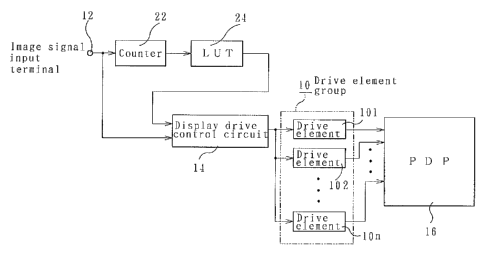
AC type PDP display device has plural drive elements (101,
102, ~~~ lOn) as shown in Figure 2. The respective drive
elements 101, 102, ~~~ lOn drive the plural pixels of PDP16 by
the drive control signal from a display drive control circuit
14 based on the image signal as input into the image signal
- 2/25 -
,~ ' 2i81~11
input terminal 12. This type of method was however
problematical in that the load as against the drive element
and the emission luminance differ when the drive voltage
(sustaining voltage and address voltage, for instance) is
applied to all the plural pixels whose drive is taken charge
of by one drive element, that is when the pixels are
discharged, and when it is supplied only to a part of the
pixels.
Conventionally attempts had been made to solve such a
problem by enhancing the capacity of the individual drive
elements or by mitigating the load to individual drive
elements through an increase of the number of the drive
elements. However, this conventional approach was
disadvantageous in that though the event of differential
emission luminance characteristic can be moderated, it cannot
be annihilated and that a large capacity of drive elements had
to be prepared. Further the number of drive elements
required was too large.
The conventional method was also problematical in that
when such display device as shown in Figure 2 displays a multi-
tone image by the ADS subfieId method, the tonal
characteristic worsens. Let us consider, for example, an
image where the most of displayed image is composed of the
image level "127" (01111111 by 8-bits binary notation) and the
small remaining area is composed of an image level "128"
(10000000 by 8-bits binary notation). V9hen the display load
factor of MSB (Most Significant Bit) subfield is compared with
- 3/25 -
L
L ~
that of the subfield other than MSB, the former is smaller
than the latter. It was unsustainable because this
difference in load factor raised the emission luminance
characteristic and worsened the tonal characteristic.
To solve such problematical points as above, the
applicant has already proposed such a circuit as shown in
Figure 3. That is, a display area detect circuit 20 is
inserted between an image signal input terminal 12 and a
display drive control circuit 14. The display area detect
circuit 20 detects the display area for every certain duration
(for e$ample, one frame or one subfield) based on the image
signal as input into the image signal input terminal 12 to
control the number of the sustaining pulses (drive pulses) in
response to the detected area.
More concretely, the display area detect circuit 20
comprises a display load factor detect circuit (a counter, for
instance) that detects the display load factor for a certain
duration and the sustaining pulse control circuit [LUT (Look
Up Table), for instance] that controls the number of
sustaining pulses, sustaining voltage or sustaining current
based on the output detected by the display load factor detect
circuit. The emission luminance characteristic can thus be
maintained constant irrespectively of the display load factor
of the display panel. This configuration further prevents
the deterioration of the tonal characteristic due to the
subfield drive method
However, the circuit as shown in Figure 3 was somewhat
- 4/25 -
.
' ~ 2181211
problematical in that the configuration of the display area
detect circuit 20 becomes complicated when one frame of the
PDP16 is time-shared into eight display durations (subfields)
corresponding to 8-bits display tones and the number of the
sustaining pulses of the respective divided display durations
are weighted to display 256 tones of image. This is because
we need eight display load factor detect circuits and eight
sustaining pulse control circuits for as many subfields. In
Figure 3, the numeral 10 indicates the group of drive elements
representing all the drive elements 101, 102,~~~ lOn as shown
in Figure 2.
BRIEF SUI~M~ARY pF THE INVENTION
The first purpose of the present invention is to provide
a drive circuit for the display device that allows for an
image display with constant emission luminance characteristic
despite the largeness of the display Ioad factor. In this
context the display load factor means the proportion of the
drive pixel number (number of lighted up pixels) occupies in
the total number of pixels for certain duration (for example,
one frame, one subfield or one line).
The second purpose of this invention is to prevent the
degradation of the tonal characteristic due to the subfield
drive method when it is used in a display device that displays
multi-tone image.
The third purpose of the invention is to provide a drive
circuit for a display device that can simplify the
- 5/25 -
1
configuration of the display area detect circuit.
In a display device intended to achieve the first purpose
of the invention where plural drive elements take respectively
charge of the driving of the plural pixels and the display
luminance changes as changes the number of the sustaining
pulses provided from each drive element to the display panel
based on the input image signal, provided are the display load
factor detect means that detects the display load factor for
certain duration based on the input image signal, the
sustaining pulse control means that controls the sustaining
pulse number based on the detecting output of said display
load factor detect means that detects the display load factor
(number of drive pixels, for instance) for every certain
duration (for example, one frame or one subfield), said
sustaining pulse control means controlling the number of
sustaining pulses based on said detecting output thereby
maintaining constant the luminance characteristic of the
display panel. This control increases the number of
sustaining pulses when the display load factor is large since
the load against the drive element is large, while it
decreases the same number when the same factor is small since
the same load is small.
In order to achieve the second purpose, this invention
adopts, as the display device, such display device as displays
multi-tone image by subfield drive method; as the display load
factor detect means, the counter that counts up the number of
drive pixels for one of every display duration out of one
- 6/25 -
218111
screen display duration (for example, one frame) and one
division display duration (for example, one subfield) ; and as
the sustaining pulse control means, the sustaining pulse
control circuit that controls the number of sustaining pulses
based on the counted value of the counter. The counter
accumulates the number of the drive pixels for every display
duration based on the counted value, and the sustaining pulse
control circuit controls the number of sustaining pulses to be
provided to the display panel.
Such configuration as above of this invention allows to
display image with constant luminance characteristic despite
the variation of the display load factor; that is, the
luminance characteristic of the display panel can be
maintained constant by the sustaining pulse control means that
controls the number of sustaining pulses based on the
detecting output of the display load factor detect means, and
further by the sustaining voltage and current control means
that controls the sustaining voltage or current based on the
detecting output of he display load factor detect means.
If this display device as adopted can display the multi-
tone image by the subfield drive method, then the
deterioration of tonal characteristic due to the subfield
drive method can be prevented; that is, the luminance
characteristic of the display panel is maintained constant by
the control, by the sustaining pulse control means, of the
sustaining pulse number based on the detecting output of the
display load factor detect means.
- T/25 -
a
i
Let us consider, for example, an image where the most of
displayed image is composed of the image level "127" (01111111
by 8-bits binary notation and the small remaining area is
composed of an image level "128" (10000000 by 8-bits binary
notatiox~. Under these conditions the control is made so
that the number of sustaining pulses is reduced for the
subfield of MSB that has a small display load factor, and it
is increased for any subfield other than MSB that has a large
display load factor. Or else the control reduces the number
of sustaining pulses for MSB subfield without changing it for
any subfield other than MS18. The degradation of the
luminance characteristic because of the subfield drive method
can thus be prevented
A display device intended to achieve the third purpose of
the invention, has plural drive elements, the respective drive
elements taking charge of the driving of plural pixels, one
screen display duration of the display panel being time-shared
into such display duration as corresponding to the display
tone, the multi-tone image being displayed by weighting the
sustaining pulse of respective divided display duration, n-
bits (n being any integer not Less than 2) of input image
signal is converted into m-bits (m5n-1) of image signal, and
at the same time provided are an intermediate display means
that looks for intermediate level from neighboring drive level
and a display area detect means that controls the sustaining
pulses so that the display area is detected for every constant
duration based on the m-bits image signal of the half tone
- 8/25 -
218111
display means and that the luminance characteristic of said
display panel is maintained constant on the basis of this
detecting output.
Said display area detect means maintains constant the
luminance characteristic of the display panel by detecting the
display load factor (for example, the number of drive pixels)
for every certain duration (one frame or one subfield, for
instance) and controlling the sustaining pulses
correspondingly, and prevents, at the same time, the
deterioration of the tone characteristic due to the subfield
drive method. Because the halftone display means concerts
the n-bits input image signal into m-bits one (m=n-1), and
looks for the intermediate level from neighboring drive level
to output it at the display area detect means, the
conventional number n can be reduced to m of the display load
factor detect circuits (counter, for instance) that constitute
the display area detect means and of the sustaining pulse
control circuit (BUT (Look Up Table), for instance].
This invention provided, by means of such a configuration
as above, a display area detect means that detects the display
area for every certain duration (one frame, for instance) and
controls the sustaining pulses so that the luminance
characteristic of the display panel can be maintained constant
based on the detecting output, the image display can be made
with constant luminance characteristic despite the changing
display load factor (number of drive pixels) and that the
deterioration of tone characteristic due to the subfield drive
- 9/25 -
21~1~13
method (ADS subfield, for instance) can be prevented.
Since further the halftone display means that converts
the n-bits input image signal into m-bits (m5n-1) one and
obtains the intermediate level from the neighboring drive
level, can convert the display area detect means from n-bits
into m-bits, the configuration of the display area detect
means can be simplified consequently. When, for example, the
display area detect means are made to comprise the display
load factor detect circuit (for example, counter) that detects
the display load factor for every certain duration and the
sustaining pulse control circuit (for example, LUT), the
number of the display load factor detect circuits and that of
the sustaining pulse control circuit can be reduced from n to
m (for example, for so many subfields).
Other and further objects of this invention will be
obvious upon am understanding of the illustrative embodiments
about to be described.
BRIEF DESCRIPTION OF THE DRAWINGS
Figure 1 (a) represents a drive sequence of the ADS
subfield method
Figure 1 (b) depicts a drive waveform of the ADS subfield
method.
Figure 2 is a block diagram showing a conventional drive
circuit of display device.
Figure 3 is a block diagram of the drive circuit of the
display device previously proposed by the applicant.
- 10/25 -
~
z~s~z~ ~
Figure 4 is a block diagram showing the first embodiment
of the drive circuit of the display device according to this
invention.
Figure 5 is another block diagram showing the second
embodiment of the drive circuit of the display device
according to this invention.
Figure 6 is a block diagram showing an example of the
sustaining voltage/current switching circuit as shown in
Figure 5.
Figure 7 is another block diagram showing the third
embodiment of the drive circuit of the display device
according to this invention.
Figure 8 (a) another block diagram showing the fourth
embodiment of the drive circuit of the display device
according to this invention.
Figure 8 (b) is a block diagram the error variance
circuit, an example of the halftone display circuit as shown
in Figure 8 (a).
DETAILED DESCRIPTION
Now the first embodiment of this invention will be
illustrated referring to Figures 4. In Figure 4, parts
corresponding with in Figure 2 designate same reference symbol.
The numeral 12 represents an image signal input terminal.
Sequentially connected to the terminal 12 are a display drive
control circuit 14, a drive element group 10 (101, 102, ~~~ lOn)
and PDP 16 in this order. As is the case with the
- I1/25 -
z~s~z> >
conventional one, said display drive control circuit 14 drives
and controls the drive element group 10 based on the image
signal (image data) input in the image signal input terminal
12, and displays the multi-tone image by ADS subfield.That is,
it time-divides one frame of PDP 16 into plural (8, for
instance) subfields and weights the sustaining pulse number of
each subfield to display the multi-tone image (for example, 8-
bits 256 tone image).
Coupled to said imagesignal input terminal 12 is a
counter 22 as an example of display load factor detect means,
which counts the number of drive pixels (display area) for
every frame or subfield to output the counted value.
Connected on the output side of said counter 22 is the
LUT (Look Up Table) 24 as an example of the major element
constituting the sustaining pulse control means, which is made
up of ROM (Read Only Memory) for example. The LUT 24 stores
beforehand in memory the number of sustaining pulses for the
drive pixels for every one frame or one subfield in order to
maintain constant the luminance characteristic of said PDP 16
irrespectively of the largeness of display load factor, the
content of which can be output with the counted value of said
counter 22 as address (heading). The data to be stored
beforehand in said LUT 24 is obtained from the characteristic
data measured of the relationship between the image signal and
the emission luminance of the~PDP 16 that displayed the multi-
tone image by ADS subfield, with each of the drive element
group 10 taking charge, for instance, of the driving of
- 12/25 -
2181211
plural pixels of the PDP 16.
Said display drive control circuit 14 drives and controls
the drive element group 10 using the sustaining pulse number
as output from said LUT 24, and maintains always constant the
luminance characteristic of the PDP 16 despite the largeness
of the display load factor.
Now the action of the drive circuit in Figure 4 will be
explained
(a) Based on the image signal as input into the image
signal input terminal 12, the counter 22 counts up the number
of drive pixels (display area) for every one frame or one
subfield and outputs the counted value to the LUT 24.
Let us consider, for example, an image where the most
of displayed image is composed of the image level '127"
(01111111) and the small remaining area is composed of an
image level '128' (10000000). The MSB subfield has a small
counted value because its drive pixel number, consequently the
display load factor is small, while the subfield other than
MSB has a great counted value because its drive pixel number,
consequently the display load factor is great.
(b) The display drive control circuit 14 receives, from
the LUT 24, the number of sustaining pulses to maintain
constant the luminance characteristic with the counted value
of the counter 22 as an address, controls the drive element
group 10 using this sustaining pulse number, and maintains
constant the luminance characteristic of the PDP 16. Let us
consider, for example, an image where the most of displayed
- 13/25 -
'~, .
image is composed of the image level "127" (01111111 by 8-bits
binary notation) and the small remaining area is composed of
an image level "128" (10000000 by 8-bits binary notation).
Since the counted value of the MSB subfield is smaller than
that of the subfield other than MSB, it is so controlled that
the number of the sustaining pulses of the MSB subfield is
reduced and the number of the sustaining pulses other than MSB
subfield is increased. Another control is that the
sustaining pulse number of MSB subfield is reduced without
changing that of the subfield other than MSB. Thus, the
luminance characteristic of the PDP 16 can be maintained
constant irrespectively of the display load factor.
Figures 5 and 6 explain the second embodiment of this
invention, where the numeral 22 represents the counter as an
example of the display load factor detect means. The counter
22 is so designed as to count the drive pixel number (display
area) for every one frame or subfield based on the image
signal as input into said image signal input terminal 12 to
output the counted value.
Coupled on the output side of said counter 22 is a
sustaining voltage/current set circuit 26 as an example of the
sustaining voltage/current control means, which sets and
outputs either the sustaining voltage or sustaining current to
the drive pixels for every one frame or one subfield to
maintain constant the luminance characteristic of the PDP 16
irrespectively of the largeness of the display load factor
based on the counted value of said counter 22.
- 14/25 -
21812_11
For these set data, the respective drive element groups
take charge of the driving of the plural pixels of PDP 16,
and the characteristic representing the relationship between
the image signal and emission luminance is measured for the
PDP 16 that displayed the multi-tone image by ADS subfield
method. The set data is obtained from these data measured
Said sustaining voltage/current set circuit 26 has been
so designed that it does output by setting different voltage
levels of voltage 1, voltage 2,~~~ voltage n, for instance,
based on the counted value of said counter 22.
Connected to the output side of said sustaining voltage/
current set circuit 26 is a-display drive control circuit 14,
on the other input side of which is connected the image signal
input terminal 12. The display drive control circuit 14
switches, drives and controls the sustaining voltage/current
switch circuit group 30 (301, 302,~~~ 30n) based on the image
signal as input into said signal input terminal 12 and the
sustaining voltage or current as set by the sustaining voltage
/current set circuit 26, and drives and control the drive
element group 10. At the same time it performs the multi-
tone image display by ADS subfield method with the PDP 16 (not
shown) as coupled with the output side of the drive element
group 10, and maintains always constant the luminance
characteristic of the PDP 16 without regard to the largeness
of the display load factor.
The foregoing sustaining voltage/current switch circuit
30 consists, for example, of such analog switch as shown in
- 15/25 -
'~ 218111
Figure 6. It has been so built up that the switching action
based on the sustaining voltage set signal and the drive
control signal from said display drive control circuit 14 sets,
at the sustaining voltage/current set circuit 26, and switches
the different voltage levels of voltage 1, voltage 2,~~~
voltage n as input through the intermediary of said display
drive control circuit 14.
Referring now to Figure 5 the function of the second
embodiment of this invention will be described now.
(a) The counter 22 will count the drive pixel number for
every one frame or one subfield based on the image signal as
input into the image signal input terminal 12, and output the
counted value to the sustaining voltage/current set circuit 26.
Let us consider, for example, an image where the most of
displayed image is composed of the image level "127" (01111111
by 8-bits binary notation) and the small remaining area is
composed of an image level "128" (10000000 by 8-bits binary
notation). The MSB subfield has a small counted value
because its drive pixel number, consequently the display load
factor is small, while the subfield other than MSB has a great
counted value because its drive pixel number, consequently the
display load factor is great.
(b) The sustaining voltaae/current get cirr"it 7a rar
and outputs the sustaining voltage or sustaining current based
on the counted value of the counter 22. The display drive
control circuit 14 switches, drives and controls the
sustaining voltage/current switch circuit group 30 based on
- 16/25 -
the image signal as input into the image signal input terminal
12 and the set data as set by the sustaining voltage/current
set circuit 26, and drives and control the drive element group
10. At the same time it conducts the multi-tone image
display at the PDP 16 by ADB subfield method, and maintains
constant the luminance characteristic of the PDP 16.
Let us consider, for example, an image where the most
of displayed image is composed of the image level "127"
(01111111) and the small remaining area is composed of an
image level "128" (10000000). Since the counted value of the
MSB subfield is smaller than that of the subfield other than
MSB, it is so controlled that the number of the sustaining
pulses of the MSB subfield is reduced and the number of the
sustaining pulses other than MSB subfield is increased
Another control is that the sustaining voltage or sustaining
current of MSB subfield is reduced without changing that of
the subfield other than MSB. Thus, the luminance
characteristic of the PDP 16 can be maintained constant
irrespectively of the display load factor.
when, for instance, the luminance characteristic of PDP
16 is made constant by the control of sustaining voltage
irrespectively of the display load factor, the sustaining
voltage of the MSB subfield is changed over from the voltage 3
as shown in Figure 6 into smaller voltage 2.
Figure 7 explains the third embodiment of this invention.
The numeral 22 symbolizes the counter group as an example
of the display load factor detect means, The forgoing
- 19/25 -
respective counters 221, 222, ~~~ 22n count up the drive pixel
number (display area) for every one line based on the image
signal as input in said image signal input terminal 12 to
output the counted value.
Connected to the respective output sides of said counter
group 22 is the sustainingvoltage/current set circuit group
26 (261, 262, ~~~ 26n) as an example of the sustaining voltage
/current control means, which sets and outputs the sustaining
voltage or current for the drive pixels For every one line in
order to maintain constant the luminance characteristic of PDP
16 irrespective of the largeness of the display Load factor.
These set data are obtained from the measurements of the
characteristic representing the relationship between the image
signal and emission luminance of the PDP 16 that displayed the
multi-tone image by the-ADS subfield method with the
respective elements of the drive element group 10 taking
charge of the driving of the 1-line pixels of PDP I6.
Coupled to the respective output sides of the aforesaid
sustaining voltage/current set circuit 26 is the display drive
control circuit group 14 (141, 142, ~~~ 14n), to the input
sides of which is coupled the image signal input terminal 12.
Each of the display drive control circuit group 14
switches, drives and controls- the sustaining voltage/current
switch circuit group 30 (301, 302, ~ ~ ~ 30n) on the basis of
the image signal as input in said image signal input terminal
12 and the sustaining voltage or sustaining current as set by
the sustaining voltage/current set circuit group 26. At the
- 18/25 -
2181211
same time it drives and controls the drive element group 10,
and displays multi-tone image by ADS subfield method at the
PDP 16 as coupled with the output side of the drive element
group 10 to maintain always constant the luminance
characteristic of the PDP 16 irrespectively of the largeness
of the display load factor.
The function of the third embodiment of this invention
will be explained now referring to Figure 7.
(a) The counter group 22 counts up the number of drive
elements for every one linebased on the image signal as input
in the image signal input terminal 12, and outputs the counted
value to the sustaining voltage/current set circuit group 26.
Let us consider, for example, an image where the most
of displayed image is composed of the image Level '127"
(01111111) and the small remaining area is composed of an
image level "128" (10000000). The MSB subfield has a small
counted value because its drive pixel number, consequently the
display load factor is small, while the subfield other than
MSB has a great counted value because its drive pixel number,
consequently the display load factor is great.
(b) The sustaining voltage/current set circuit group 26
sets and outputs the sustaining voltage or sustaining current
based on the counted value of the counter group 22. The
display drive control circuit group 14 switches, drives and
controls the sustaining voltage/current switch circuit group
30 based on the image signal as input into the image signal
input terminal 12 and the set data as set by the sustaining
- 19/25 -
2181211
voltage/current set circuit group 26, and drives and controls
the drive element group 10. At the same time it conducts the
multi-tone image display at the PDP 16 by ADB subfield method,
and maintains constant the luminance characteristic of the PDP
16.
Let us consider, for example, an image where the most
of displayed image is composed of the image level "12T
(01111111) and the small remaining area is composed of an
image level "128" (10000000). Since the counted value of the
MSB subfield is smaller than that of the subfield other than
MSB, it is so controlled that the number of the sustaining
pulses of the MSB subfield is reduced and the number of the
sustaining pulses other than MSB subfield is increased.
Another control is that the sustaining pulse number of MSB
subfields is reduced without changing that of the subfield
other than MSB. Thus, the luminance characteristic of the
PDP 16 can be maintained- constant irrespectively of the
display load factor.
In the foregoing first, second and third embodiments, an
explanation was made on the case where this invention is used -
for the display device that displays multi-tone image by the
ADS subfield method, but the invention is not limited to this
type of embodiment. The present invention can be used at
least and also to a display device where the respective drive
elements take charge of the driving of plural pixels whose
display luminance changes as changes the number of sustaining
pulses, sustaining voltage or sustaining current.
- 20/25 -
i I
Now the fourth embodiment of this invention will be
explained referring to Figures 8 (a) and 8 (b).
Connected to the image signal input terminal 12 is the
display area detect circuit group 20 (20I, 202,~~~ 20m)
through the intermediary of the half tone display circuit 31,
while the display drive control circuit 14, the drive element
group 10 and PDP 16 are sequentially connected in this order
to the output side of the display area detect circuit group
20m.
Figure 8 (b) shows up an error variance circuit as an
example of aforesaid half tone display circuit 31. The error
variance circuit consists of a vertical adder 32 that adds
vertical reproduced error to n-bits input image signal as
input into the image signal input terminal 12, a horizontal
adder 34 that adds a horizontal reproduced error to the output
signal of this vertical adder 32, an error detect circuit 36
that outputs an error weighting signal by detecting and
weighting the difference between the output signal of the
horizontal adder 34 and the correction data as preset at ROM,
among others, a h-line delay circuit 38 that delays by h-lines
the error weighting signal as output from the error detect
circuit 36 and outputs it to the vertical adder 32, d-dot
delay circuit 40 that delays by d-dots the error weighting
signal as output from the error detect circuit 36 and outputs
it as reproduced error to the horizontal adder 34, and a bit
convert circuit 44 that converts the n-bits image signal as
output from the horizontal adder 34 into m-bits (men-1) image
- 21/25 -
.,
2
signal and outputs it to the aforesaid display area detect
circuit 20 through the intermediary of the output terminal 42.
Said display area detect circuit 20 comprises a display
load factor detect circuit (counter, for instance) that
detects the display load factor for every certain duration
(one frame, one subfield or one line) and sustaining pulse
control circuit (for example, LUT [Look Up Table]} that
controls the sustaining pulse (for example, pulse number,
sustaining voltage or sustaining current) so that the
luminance characteristic of PDP can be maintained constant on
the basis of the detect output of the display load factor
detect circuit. More materially, the LUT as an example of
the sustaining pulse control circuit stores beforehand in
memory the data of sustaining pulse (for example, pulse number,
sustaining voltage or sustaining current) for the drive pixels
for every one frame, one subfield or one line in order to
maintain constant the luminance characteristic of PDP 16
irrespectively of the largeness of the display load factor
with the counted value of the counter as an example of the
display load factor detect circuit, as an address,
The foregoing display drive control circuit 14 drives and
controls the drive element group 10 using the data of
sustaining pulse (for example, pulse number, sustaining
voltage or sustaining current) as obtained from said display
area detect circuit 20 and maintains always constant the
Luminance characteristic o~ PDP 16 irrespective of the
largeness of the display load factor.
- X2/25 -
' ~ 2181211
Now the function of the embodiment shown in Figure 8 will
be explained.
(a) The half tone display circuit 31 adds vertical and
horizontal reproduced errors to the n-bits input image signal
as input, by the adders 32 and 34 into the image signal input
terminal 12, while the error detect circuit 36 detects and
weights the difference between the output signal of the
horizontal adder 34 and the correction data. The delay
circuits 38 and 40 delay by h lines and d dots the error
weighting signal as output from the error detect circuit 36 to
output it to the adders 32 and 34. The bit convert circuit
44 converts the n-bits signal into m-bits (msn-1} image signal
and outputs it to the display area detect circuit 20 through
the intermediary of the output terminal 22.
Thus the half tone display circuit 31 takes as an error
the difference between the image level to be displayed and the
drive level as displayed to disperse it over the image in both
horizontal and vertical directions. The half tone display by
such error variance will reduce the number of the subfields as
driven by the downstream subfield driving method (for example,
ADS subfield method) and compensates for the tones
corresponding to this reduction by the half tone, that is,
maintains the number of tones to be displayed.
(b) The display area detect circuit 20 detects the
display load factor for every certain duration (for example,
one frame) based on the m-bits image signal as output from the
half tone display circuit 31, counts up the number of drive
- 23/25 -
. ~ zas~z~ ~
pixels by the counter and controls the sustaining pulse so
that the luminance characteristic of PDP 16 can be maintained
constant with this counted value as, for example, an address
on the basis of the detect output (for example, outputs the
number of sustaining pulses, the content of the address from
the LITi~ .
Let us consider, for example, an image where the mast
of displayed image is composed of the image level "12T
(01111111) and the small remaining area is composed of an
image level "128' (10000000). Since the display loaf factor
(counted value, for instance) of the MSB subfield is smaller
than that of the subfield other than MSB, it is so controlled
that the number of the sustaining pulses of the MSB subfield
is reduced and the number of the sustaining pulses other than
MSB subfield is increased Another control is that the
sustaining voltage or sustaining current of MSB subfield is
reduced without changing that of the subfield other than MSB.
Thus, the luminance characteristic of the PDP 16 can be
maintained constant irrespectively of the display load factor.
(c) The display drive control circuit 14 controls the
drive element group 10 using the sustaining pulses as output
from the display area detect circuit 20, displays multi-tone
image by the subfield drive method (ADS subfield method) at
the PDP 16, and maintains constant the luminance
characteristic of the PDP 16.
The foregoing fourth embodiment has been described
adopting a vase where an error variance circuit is used as an
- 24/25 -
29~~~1;1
example of the half tone display means, but this invention is
not limited to this embodiment. Any embodiment will do if n-
bits input image signal can be converted into m-bits (m~n-i)
one and the intermediate level thereof can be obtained from
the neighboring drive level. For instance, the configuration
of the embodiment may use such means as FRC Frame Rate
Control).
In the foregoing embodiments, the first to the fourth, we
explained the case where the display panel of the display
device is PDP, but this invention is not limited to this. The
invention may include such a case where the display panel is
LCDP display device.
- 25/25 -