Note: Descriptions are shown in the official language in which they were submitted.
2181316
-2- C-CCD-0153
BACKGROUND OF THE INVENTION
IC cards, which are of about the same width and length as a
typical credit card, have dimensions defined by PCMCIA (Personal
Computer Memory Card International Association). Such cards have a
width and length of 54 mm and 85.6 mm, respectively, with three different
types having thicknesses of 3.3 rnm, 5 mm, and 10.6 mm. Recent cards
allow connection of the card to a local area network (LAN) by providing a
receptacle connector at the rear of the IC card. An adapter cable
assembly has a plug connector at its front end that plugs into the
receptacle connector at the rear of the card. U.S. patents 5,387,110 and
5,411,402 describe plug connectors of this type, which have latches at their
middles.
Newer IC cards require greater numbers of contacts. A
latching mechanism for retaining a plug connector to the rear of the card,
may occupy space that otherwise could hold several contacts, which
makes even less space available. When the plug and receptacle contacts
mate, electrical ground planes or grounds of the plug and receptacle
connectors and/or their corresponding circuit boards must be connected.
tf grounding is to occur through regular pin and socket contacts, then such
grounding contacts may not have sufficient current-carrying capacity, and
they waste space that could otherwise be occupied by signal contacts.
Also, there may be a substantial buildup of static electricity in the plug or
receptacle, and a spark created as contacts closely approach each other,
could damage adjacent contacts, especially in the case of pin contacts
wherein there is no insulation between the free ends of adjacent pins. Plug
and receptacle connectors which facilitated grounding to each other while
minimizing the amount of space required for the grounding connections
<vPfiO~)Tf'.CCr.C0153.PCT Jvne 1t. 1986
CA 02181316 1999-11-04
- 3 -
and while isolating any sparks created during mating from
signal-carrying contacts, would be of value.
SUMMARY OF THE INVENTION
In accordance with one embodiment of the present
invention, plug and receptacle connectors and their combination
are provided with means for connecting together the grounds of
the connectors and/or corresponding circuit boards in a manner
that minimizes space required for mating grounding terminals
while protecting signal contacts from sparks. The receptacle
connector includes a grounded sheet metal shield surrounding
the dielectric receptacle housing, while the plug connector has
a grounded member that engages the receptacle shield during
mating. The receptacle shield has a tab that is joined, as by
soldering, to a grounded trace on its corresponding circuit
board, while the plug grounded member has a tab that is joined
to a grounded trace on its corresponding circuit board. The
plug grounded member has a terminal portion that lies in a
groove at a side of the plug dielectric housing, with the plug
terminal portion having a part that projects slightly from the
groove to engage the shield. The shield includes an elongated
strip that is bent about 180' and which engages the projecting
part on the plug ground member.
The invention may be summarized according to one
broad aspect as a plug connector for mating with a receptacle
connector, comprising: a dielectric plug connector housing
which is elongated in a lateral direction and which has
laterally spaced opposite side walls; a plurality of plug
contacts arranged in at least one laterally extending row and
mounted on said housing; a circuit board attached to said
housing, said circuit board having a board front portion and
having at least one laterally-extending row of conductive
contact traces on said board front portion, said contacts
CA 02181316 1999-11-04
- 3a -
having tails joined to said contact traces, said circuit board
also having at least one ground trace; each of said housing
opposite side walls has a recess facing away from said row of
contacts, and including a pair of plug ground members each
having a forward terminal portion lying in one of said housing
recesses with each of said forward terminal portions having a
contact part extending in a bend that projects laterally beyond
adjacent portions of the corresponding housing side wall, and
with each plug ground member having a rear portion joined to
one of said circuit board ground traces.
According to another broad aspect the invention
provides a receptacle connector comprising: a dielectric
receptacle housing having a hollow rear end, a top, a bottom,
and laterally-spaced opposite sides; a plurality of receptacle
contacts arranged in at least one laterally extending row, said
contacts being mounted on said housing and having pin-like free
rear ends lying in said hollow rear end; a circuit board
connected to said housing, said circuit board having a rear
portion and having at least one laterally-extending row of
conductive contact traces at said rear portion, with said
contacts having tails joined to said contact traces, said
circuit board also having a ground trace, of greater lateral
width than any of said contact traces, said housing having a
latch-receiving middle region, said row of traces being
interrupted at said middle region with said ground trace lying
at the same lateral position as said interruption in said row
of traces; a sheet metal shield extending on the top, bottom
and laterally-spaced opposite sides of said housing, said
shield having a middle lying about halfway between said
opposite sides and having a portion joined to said ground trace
on said circuit board.
According to yet another aspect the invention
provides a receptacle connector for mating with a plug
CA 02181316 1999-11-04
- 3b -
connector that has a grounded member, comprising: a dielectric
receptacle housing which is elongated is a lateral direction
and which has a hollow rear end, a top, a bottom, and
laterally-spaced opposite sides; a plurality of receptacle
contacts arranged in at least one laterally extending row, said
contacts being mounted on said housing and having free rear
ends lying in said housing hollow rear end; a circuit board
connected to said housing, said circuit board having a rear
portion and having at least one laterally-extending row of
conductive contact traces at said rear portion, with said
contacts having tails joined to said contact traces, said
circuit board also having a ground trace; a sheet metal shield
extending on the top, bottom and opposite sides of said
housing, said shield having a portion electrically connected to
said ground trace on said circuit board; said sheet metal
shield including a strip-shaped sheet metal portion lying in
vertical planes at a location which is primarily laterally
spaced from an end of said row of contacts, said strip-shaped
sheet metal portion being electrically connected to said ground
trace on said circuit board, and said strip-shaped sheet metal
portion forming a grounding terminal positioned to engage said
plug connector grounded member.
The novel features of the invention are set forth
with particularity in the appended claims. The invention will
be best understood from the following description when read in
conjunction with the accompanying drawings.
2181316
-4- C-CCD-0153
BRIEF DESCRIPTION OF THE DRAWINGS
FIG. 1 is an exploded isometric view of a portion of a
connector system which includes a plug connector that is mateable with
a receptacle connector that lies at the rear of an IC card.
FIG. 2 is an exploded sectional top view of a portion of the
system of FIG. 1.
FIG. 3 is an exploded isometric view of a portion of the
connector system of FIG. 1, showing portions of the dielectric housings
and circuit boards of the connectors.
FIG. 4 is an enlarged plan view of a portion of the plug
connector of FIG. 2.
FIG. 5 is a side elevation view of an upper shield member of
the receptacle shield of FIG. 3.
FIG. 6 is a sectional side view of the lower shield member of
the receptacle shield of FIG. 3.
FIG. 7 is a partial plan view of the lower shield member of FIG.
6.
FIG. 8 is a partial isometric view of the dielectric receptacle
housing of the receptacle of FIG. 3.
FIG. 9 is a view of a portion of the lower shield member of
FIG. 6, and showing a portion of the plug ground member of the plug
connector of FIG. 4, in the course of connector mating.
DESCRIPTION OF THE PREFERRED EMBODIMENTS
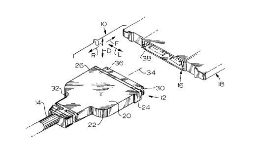
FIG. 1 illustrates a connector system i0 that includes a plug
connector 12 lying at the front of a cable 14, and a receptacle connector
16 lying at the rear of an IC card 18 of the PCMCIA type. Such IC cards
WP6011TT'CCCD0153.PCT June tt, 1986
2181316
-5- C-CCD-0153
generally have a width of 54 mm and length of 85.6 mm, and a thickness
that may range between 3.3 mm and 10.5 mm, with the particular card
illustrated being a type II card which has a thickness of 5 mm. The plug
connector has laterally opposite sides 24, 26 front and rear ends 30, 32
and a top and bottom 20, 22, and is mated to the receptacle connector by
moving the plug connector forvvardly in the direction F along a plug
connector axis 34. The connectors are symmetrical about a vertical plane
extending through the axis 34. During mating, socket contacts 36 of the
plug connector mate with pin contacts 38 of the receptacle connector.
Forward and rearward directions are indicated by arrows F, R, up and
down directions are indicated by arrows U, D, and lateral directions are
indicated by arrow L.
As shown in FIG. 2, each connector has a latch region 50, 52,
which is designed to contain a latch mechanism. A variety of latch
i5 mechanisms are available, such as those shown in U.S. patents 5,387,110
and 5,411,402. Fig. 2 indicates a latch mechanism in phantom lines, by
a latch 40 on the plug connector and a latch-receiving recess 42 on the
receptacle connector.
The plug connector 12 has a dielectric plug housing 54 with
front and rear portions 56, 58 and laterally opposite side walls 57, 58. The
rear portion 58 is connected to a plug circuit board 60. The plug
connector has two Laterally-extending rows of socket-type plug contacts 36.
The circuit board has a front portion 64 that holds a laterally (n direction
L) extending row of conductive traces 66 on both its upper and lower
faces, with the socket contacts having tails 70 that are joined to the traces
as by soldering.
WP6WTPCCCC0153.PCT Juna ii. W
2181316
-6- C-CCD-0153
The receptacle connector 16 has a dielectric receptacle
housing 80, and the card 18 includes a receptacle circuit board 82. The
receptacle connector has a row of receptacle contacts 38 with pin-type rear
ends 86. Each receptacle contact has a middle 90 anchored in the
receptacle housing 80 as by being molded in place, and has a tail 92 at its
front end. The circuit board 82 has a row of electrically conductive traces
94 to which the contact tails are joined, as by soldering. The circuit board
is shown having two rows of traces 94, 96, one for contacts of the upper
row and one for contacts of the lower row.
As shown in FIG. 3, the receptacle connector 16 includes a
sheet metal shield 100 that lies immediately above, below, and on laterally
opposite sides of the receptacle housing 80. As also shown in FIG. 8, the
receptacle housing 80 has a top and bottom 102, 104 and opposite sides
106. Referring to FIG. 3, it can be seen that the receptacle housing forms
a hollow region or hollow 110 at its rear end, and the pin-type free ends 86
of the receptacle contacts lie within the hollow. The presence of the shield
is especially important where higlh frequency signals are carried.
Applicant forms the shield with a ground receptacle terminal
or terminal portion 120 in the form of a bent elongated strip of the sheet
metal of which the shield is formed. As shown in FIGS. 6 and 7, the strip
extends from a rear edge 122 of the shield and has a substantially 180°
bend 124 near where it emerges from the end, with the rest of the strip 125
extending substantially forwardly and lying within the rest of the shield. As
indicated in FIG. 8, the dielecUic receptacle housing 80 has a slot or
groove 130 that receives the benr< elongated strip shown in FIG. 7 at 120.
The bent strip or receptacle ground terminal provides a smooth surface
WP6PITT'CCC00153.PCT June 1 t, t986
~ 2181316
-7- C-CCD-0153
and also adds resilience to aid in contacting a grounded terminal portion
of the plug connector.
As shown in FIG. 3, the plug connector housing 54 has a top
and bottom and opposite sides, and has a recess or groove 140 in each
of its sides. A plug ground member 142 has a forward terminal portion
144 lying in the groove, with a bent contact part 146 thereof projecting
sidewardly out of the groove. The sheet metal of the forward terminal
portion 144 lies in substantially vertical planes, and has a greater vertical
height than its thickness. When the connectors mate, the plug housing 54
fits within the hollow 110 at the rear of the receptacle connector housing.
During such mating, the projecting part 146 of the plug ground member
engages the bent strip 120 formed on the shield of the receptacle
connector. Such engagement occupies very little of the lateral width of the
connector, which is usually less than the space that would be occupied by
a pin-type terminal 84 (plus the space required around it). Also, any
sparks created during mating of the projection 146 with the bent strip 120
is largely shielded from the signal-carrying contacts by the dielectric plug
housing 54. The grounded terminal portions 144, 120 have a large cross-
section which is usually greater than that of the pin free ends 86 to carry
large grounding currents. Furthermore, the grounding of the receptacle
occurs at the strip 120 which is ',part of the rest of the sheet metal shield
100, so that it is not necessary to provide a connection between a pin type
contact and the shield or to make any solder or weld joints therealong.
The receptacle circuit board has an electrically grounded
receptacle trace 160. The sheet metal shield 100 has a middle that is
provided with a tab 162 which is bent and which has a ground terminal
portion 164 that is joined to the grounded trace 160 as by soldering
wPSwrncccoo,s3.acr ~~~e ". ,sss
~ 2181316
-8- C-CCD-0153
thereto. As can be seen in FIG. 2, the grounded trace 160 lies immediately
forward of the latch region 52 that would be occupied by a cavity 42 to
which a latch on the plug connector would latch. Accordingly, the space
at the trace 160 could not otherwise be occupied by contact pads so long
as a latch-receiving cavity lies at the middle of the connectors. By
applicant providing the grounded trace 160 on this location, the grounded
trace 160 does not occupy space that otherwise would be used, and a
wide large current-carrying capacity tab can connect to the grounded
trace.
As shown in FIG. 3, the plug ground member 142 has a rear
portion 170 that forms a tab 172 which is joined to an electrical ground
plug trace 174 on the plug circuit board 60. The tab can lie at 172A to
connect to the bottom face of a higher circuit board.
It can be seen from FIG. 3, that the shield 100 has upper and
lower shield members 170, 172. The upper shield member is provided
with a pair of locking ears 175 that project into locking slots formed in the
lower member. As a result, the shield can be readily placed around the
receptacle connector housing 80 by moving the lower shield up and the
upper shield down, until the ears 175 snap into the slots 176, at which time
the tab ground portion 164 will lie against the circuit board ground trace
160.
Both the plug housing 54 and receptacle housing 80 are of
largely parallelepiped shape, with largely parallel top and bottom surfaces
and largely parallel laterally-spaced opposite sides. The hollow 110 is
preferably formed so that it has a narrow upper end 180 and a slightly
wider lower end 182, to form a polarizing keyway that receives a
correspondingly polarized plug connector housing 54. Applicant prefers
WP60JTTGCC00153.PCT Jmro t t. 1996
2181316
-9- C-CCD-0153
to make the grounding connection at the opposite ends of the wider lower
housing ends, where the grounding contacts are spaced slightly more from
the signal-carrying contacts.
In a system that applicant has designed, the shield 100 had
a lateral width of 1.14 inch, a height of 0.17 inch, and a front-to-rear
length
(not including tab 162) of 0.314 finch. The upper and lower interrupted
rows of contacts each included eighteen contacts spaced at a 0.050 inch
pitch.
Although terms such as "upper", "lower", etc. are used to aid
t0 in the description of the parts as illustrated, the connectors and other
parts
can be used in any orientation with respect to Earth's gravity.
Thus, the invention provides plug and receptacle connectors
and the combination of the connectors and circuit boards of a plug and an
electronic device such as an IC card, with an enhanced electrical
grounding arrangement. The receptacle connector is provided with an
electrically grounded sheet metal shield, while the plug connector is
provided with a plug grounding member for engaging the shield. The
engaging portions preferably lie at opposite sides of the respective
housings, and preferably within the wider keyways or keys thereof. The
shield has a tab that is joined to a grounded conductive trace on a circuit
board associated with the receptacle connector. The plug grounding
member has a rear portion forming a tab that is joined to a grounded trace
on the plug circuit board. The plug grounding member preferably has a
forward terminal portion lying in a groove at the side of the dielectric plug
housing, and has a bent laterally projecting portion. The shield of the
receptacle connector preferably has an elongated strip that is bent about
2181316
-10- C-CCD-0153
180° to form a terminal for engaging the corresponding terminal formed
by
the plug grounding member.
Although particular embodiments of the invention have been
described and illustrated herein, it is recognized that modifications and
variations may readily occur to those skilled in the art, and consequently,
it is intended that the claims be interpreted to cover such modifications and
equivalents.
WPfi0UT1tC~00153.PCT Jug t t. t986