Note: Descriptions are shown in the official language in which they were submitted.
CA 02181336 2002-02-08
WO 95/20772 2181336 PCT/GB95/00141
Optical Backplane Interconnect
FIELD OF THE INVENTION
s This invention relates to an optical backplane interconnect that has
particular
but not- exclusive application to optical telecommunication networks.
BACKGROUND
In order to connect all the nodes of a network to one another, a large number
ro of connections is usually required, which becomes impractical if individual
optical fibres are used to make the connections. In order to simplify the node
connections, an optical bus architecxure has been proposed in "Optical
Interconnect based on a Fibre Bus" F. MacKenzie et al - Optical and Quantum
Electronics 24 (1992) S 491-S 504. This discloses an optical bus consisting of
a
13 plurality of parallel D-section optical fibres. Connections are made to the
optical fibres by means of further D-section fibres that overlay the fibres of
the bus at a predetermined angle. As explained in the paper, the angle of
intersection determines the degree of coupling between the fibres and the
arrangement permits signals to be selectively coupled into and from the bus.
2o The connections can be anmaged in groups, to provide a modular structure.
The circuitry is arranged on separate cards that carry both optical and
electrical circuits, which are connected to the optical fibre bus and the
cards
can be arranged in a racked amngement in a similar manner to conventional
electrical printed circuit boards in a telephone exchange. Reference is also
25 directed to EP-A-0382430 which shows a similar arrangement.
However, problems have been encountered in designing an interconnect
which provides a consistent and reliable coupling to the optical fibre bus and
as a result, when cards are removed and reinserted, or inserted in different
so locations in the rack, the optical coupling to the bus may change
undesirably.
The present invention seeks to overcome these problems.
CA 02181336 2007-04-17
-2-
SUMMARY OF THE INVENTION
Accordingly, in one aspect of the present invention there is provided n
optical
backplane interconnect comprising a backplane including a plurality of optical
bus
waveguides, a connecting block provided with a plurality of optical paths to
be
aligned in a predetermined angular relationship with the bus waveguides of the
backplane so as to form optical couplings therewith and coupling means acting
between the backplace and connecting block. The coupling means is operative in
such a manner that as the connecting block is moved in a forward direction
towards
the backplane, the connecting block is caused automatically to rotate so as to
produce
self-alignment of the waveguides and the paths in said predetermined angular
relationship.
The interconnect may include a card, a support on which the backplane is
mounted,
and mounting means on the support for the card, the coupling means being
resiliently
mounted on the card and operative so that as the card is moved in the forward
direction into the mounting means the connecting block moves relative to the
card to
produce said self alignment.
The backplane may include a plurality of D-section optical fibres which in the
region
of the connecting block are generally parallel to one another, and the optical
paths in
the connecting block may include portions that are generally parallel and
spaced for
coupling with respective ones of the optical fibres, said coupling means
holding the
optical path portions at a predetermined angle relative to the optical fibres.
The card can carry optical components connected to said plurality of optical
paths.
The optical paths may themselves be defined by further D-section optical
fibres. The
coupling means may comprise a groove in the backplane and projection means on
the
connecting block, that fits into the groove. The projection means may comprise
an
elongate member that runs longitudinally of the groove, so as to hold the
connecting
block at a predetermined angle to
CA 02181336 2002-02-08
WO 9S/20772 PC'T/cB95/00141
21813,.38
-3=
the backplane. Alternatively, the projection mcans may comprise one or
more spaced members that fit into the groove. The or each spaced member
may comprise a ball received in a recess in the connecting block.
s In an alternative configuration, the channel in the backplane may be wider
than the aforesaid groove, with the optical fibres being arranged in the
channel.
The card may comprise a network card that carries both optical and electrical
io circuit components, in which case the mounting means for the card can
comprise an electrical edge connector mounted on the support to receive the
network card. The edge connector can itself be connected to an electrical bus.
In another aspect the invention includes an optical network interconnect
rs comprising: a support, a backplane mounted on the support, the backplane
including a plurality of optical fibres, a network card, an edge connector
mounted on the support to receive the network card, a connecting block
mounted on the network card and provided with a plurality of optical paths
to be coupled to the optical fibres in the bswckplane respectively, and
coupling
20 means comprising a mutually cooperating coupling member and receptacle
arruigement which provides a coupling betweea the connecxing block and the
backplane in a predetermined configuration, whereby to couple the optical
paths of the connecting block to the optical fibres in the backplane, such
that
upon insertion of the card into the edge connector, the coupling means is
25 operative to couple the connecting block to the backplane in said
predetermined configuration.
BRIEF DESCRIPTION OF THE DRAWINGS
In order that the invention may be more fully understood, embodiment
3o thereof will now be described by way of example with reference to the
accompanying drawings in which:
__....~._._._._.~...~..,~........_._.._~,_.__.__ __..._...._. _._..._.....- ---
CA 02181336 2002-02-08
WO 95/20772 218 13 36 PCT/GB95/00141
.4.
Figure 1 illustrates a known MONET optical fibre architecture;
Figure 2 shows a schematic illustration of a D-fibre cross point;
Figure 3 is a schematic illustration of an array of fibre couplings;
Figure 4 is a schematic perspective view of a rack interconnect in accordance
s with the invention;
Figure 5 is a schematic perspective view of a connecting block and backplane
for use in an interconnect in accordance with the invention;
Figure 6 is an enlarged sectional view of one of the balls shown in Figure 5;
Figure 7 is a schematic perspective view of an alternative connecting block
io configuration in which the balls are replaced by a half-rod;
Figure 8 is a schematic sectional view of an alternative optical backplane
interconnect in accordance with the invention;
Figure 9 is a sectional view of yet another embodiment of the invention;
Figure l0a is a plan view of a further embodiment of interconnect in
rs accordance with the invention;
Figure l0b is a sectional view of the interconnect shown in Figure 10a;
Figure 11 is a schematic perspective view of an alternative coupling between
the connecting block and the backplane;
Figure 12 is a schematic perspective view illustrating an alternative method
of
20 fabricating the backplane;
Figure 13 illustrates schematically mouldings which can be used to form the
backplane and connecting block for an interconnect in accordance with the
invention.
25 DETAILED DESCRIPTION
Referring to Figure 1, an optical bus architecture is shown that consists of a
bus 1 of optical fibres. An interface to the optical bus is provided by means
of network cards which carry optical and electronic sub-systems. In Figure 1,
a transmitter card 2 and a receiver card 3 are shown. This general
3o configuration is known as a MONET system (Multi-dimensional Optical
Network) and reference is directed to D. W. Smith et al, Globecon '89 Vol 1,
Paper 1.2.1, Dallas, USA. The transmitter card 2 contains a number of
CA 02181336 2002-02-08
WO 95l20772 .- PGT/GB95/00141
~.._
2181336
.S.
wavelength sourc,els 4, typirally semiconductor lasers, that provide optical
source signals to a wavelength division multiplexer (WDM) 5 which supplies
optical signals to a modulator 6 that receives control signals on line 7. An
optical space switch 8 supplies output signais to four optical paths, in the
form of optical fibres 9 that are coupled to respective fibres of the bus 1.
Similarly, the receiver card 3 includes a plurality of optical fibres 10 that
receive signals from the bus 1, connected to a space switch 11 connected to a
demodulating optical circuit 12, 13.
As will be explained in more detail hereinafcer, the cards can be selectively
connected and removed from the bus, providing for an extremely flexible
system which can be expanded and mod;ified as required. Interchangeable
cards can be designed to achieve wavelength filtering, wavelength re-routing,
1s wavelength translation (receive X1 and retransmuit data at X2) drop and
insert
(retransmit at selective channel wavelength X1) and protection switching
either
by wavelength re-routing or by wavelength tmnslation.
In order to allow the cards to be changed or reconfigured, a suitable coupling
2o between the optical fibres 9, 10 and the fibres of the bus 1 needs to be
achieved This will now be explained with reference to Figures 2 and 3. As
described in MacKenzie et al supra, optical coupling can be achieved between
adjacent lengths of so-called D-fibre that are laid in contact with one
another.
D-fibre is produced by removing the fibre cladding at the preform stage so as
25 to leave a D-shaped cross section. The preform is then drawn under special
conditions so that its geometry is maintained - see Davey ST, "High Quality
D-Fibre for Optical Telecommunications" BTTJ, Vol. No. 4 pp 3-9 1990. If
two D-fibres are arranged to overlie one another, in contact, as shown in
Figure 2, optical coupling occurs between the fibres and the degree of
3o coupling is dependent upon the angle of intersection, which in turn
controls
the coupling length. Thus, different degrees of coupling can be achieved by
setting a different angle between the fibres. As shown in Figure 3, an arrayed
~_.__.~.._._...,~ _....... .__.._,.... _ __.. _.. _.... ..._~~-- ....._ _ _
........ .. --
CA 02181336 2002-02-08
WO 95/20772 21 81336 PCT/GB95/00141
=6-
connector can be formed. The D-fibres 11, 12, 13, can be laid in parallel,
equally spaced, preformed grooves in a substrate 15, typically formed of
plastics material and are then press formed into the substrate by applying a
heated moulding plate over the D-fibres, as described in US Patent No. 5 231
682. The fibre spacing is typically 500 m. In this way, a backplane can be
formed containing the bus. Fibres 23 may similarly be formed into a
connecting block, as will be explained in more detail hereinafter.
Although arrangements of this general design have been proposed hitherto -
see F. MacKenzie et al supra, difficulties have been encountered in designing
a
io practical form of connector in which the angle of intersection of the
groups of
fibres can be maintained in a predictable and controllable way so that when
individual cards are changed, the same optical coupling occurs.
The optical backplane interconnect shown in Figure 4 provides a solution to
rs these problems. As shown in Figure 4, an optical backplane 15 which
contains four optical D-section fibres 1 which are spliced to conventional
fibres 16, 17 at opposite ends of the backplane, the splices being buried in
the
plastics material 15 of the backplane by way of protection. The backplane is
manufactured as described in our US Patent No. 5 231 682 aforesaid. The
2o backplane is also provided with an elongate channel in the form of a groove
27 that runs parallel to the D-fibres 1. The structure of the backplane can be
seen in more detail in Figure 5a.
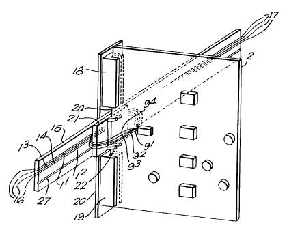
As shown in Figure 4, the card 2 is mounted adjacent the optical backplane
25 by means of a conventional electrical connectors 18, 19 mounted on a
support
bar 20 that also receives the backplane 15. The connectors 18, 19 thus grip
the card 2 and hold it physically in place. The connectors 18, 19 form
electrical contacts with electrical connections on the card 2 (not shown). The
connectors 18, 19 .;nay themselves be connected to an electrical bus (not
3o shown).
Optical connection to the optical bus fibres 1 is achieved by means of the
CA 02181336 2002-02-08
WO 95120772 rcr/cB95/OO141
21-81336
.,_
fibres 9 and a connector block 21 which is niounted transversely on edge 2a of
the cad by means of a resilient mounting clip 22. The connector block 21 is
formed in a similar manner to the backplane 15, and is shown in more detail
in Figure 5b. The optical fibres 9, which are connected to circuit components
s on the card 2, extend in a loop, as shown in Figure 4 from one side of the
card to the other through the connecting block 21. Referring now to Figure
5b, the connecting block 21 includes four parallel, equally spaced D-fibres 23
mounted in grooves (not shown) in the block 21 in the manner previously
described, having the fibres 9 spliced thereto at opposite ends, the splices
ro being buried into the block 21 to provide physical protection for the
joints.
In order to provide a predetermined alignauent of the fibres 23 of the
connection block with the fibres 1 of the backplane 15, projections in the
form of two ball bearings 25, 26 are mounted on the connecting block 21 to
15 be received into the groove 27 of the backplane 15. As shown in Figure 5b,
the baU bearings 25, 26 are arranged in a line, makes a small angle t with the
longitudinal direction of the parallel fibres 23 of the connecting block.
Thus,
this angle 46 constitutes the angle of intersection between the two sets of D-
fibres 1, 23 and thus defines the optical coupling between them.
Referring to Figure 4, it will be seen that the card 2 can be removed and
replaced by another and furthermore, additional cards can be connected to the
backplane by the provision of further card mountings (not shown). When the
card 2 is to be mounted on the backplane, the card, together with the
connecting block 21, which is mounted on the edge 2a of the card by the
resilient mountiag 22, is pushed into the electrical connectors 18, 19 to be
received in situ. As a result, the connecting block 21 is pressed in a forward
direction towards the backplane 15 and the ball bearings 25, 26 become
aligned in the groove 27 thus accurately alignin- the D-fibres 1, 23 of the
io backplane 15 and the connecting block 21. The resilience provided by the
mounting 22 urges the block 21 towards the backplane 15 to provide a reliable
contact. It has been found that when the card is removed and reinserted
_ ._.___~.......__._.. _.-..,......_....._._..__.._...~~.. ....._... .. _...
.....__...,
CA 02181336 2002-02-08
WO 95n0772 PCT/GB95/00141
2181336
8-
several times, the optical connection to the bus 1 remains substantially
constant i.e. substantially invariant of the number of times that the card is
inserted and removed. Furthermore, if the card is inserted into a further
mounting at a different location on the bus, a substantially constant optical
coupling occurs, irrespective of the location.
Figure 6 shows the action of one of the ball bearings 25 or 26 shown in
Figure 5b. The ball 25 is received in a recess 24 in the connecting block 21
and is appropriately located therein. When the connecting block 21 is pressed
io in the forward direction towards the backplane 15, the ball presses into
the
groove 17 and it can be seen that the ball will centre itself within the
groove
and the centre line of the ball is so arranged as to be below the surface of
the
backplane 15 and as a result, an accurate alignment of the connecting block 21
and the backplane 15 will occur. Furthermore, if the backplane 15 and block
is 21 are misaligned as they are pressed together, the ball will tend to seek
the
groove 27 and self-align automatically, so as to achieve the desired
alignment,
the resilience of the mount 22, allowing relative movement of the connecting
block 21 and the card 2 laterally of the forward direction, so that the
desired
alignment can be achieved.
Referring now to Figure 7, this shows a modification in which the balls 25, 26
are replac,ed by an elongate rod 28 received in the connecting block 21. This
functions in much the same way as the pair of balls 25, 26 but is received in
the entire length of the grooves 27 in the backplane 15. The rod 28 may
comprise a glass rod received in a channel in the connecting block 21 or
alternatively may comprise a moulded protrusion integrally formed into the
block 21.
Referring now to Figure 8, this shows a sectional view through the block 21
3o and the backplane 15 in which, the channel, instead of being a narrow
groove
27 is somewhat wider, forming a trough 29 with a bottom surface 30 and
inclined sidewalls 31. The connecting block 21 is provided with a mesa 32
CA 02181336 2002-02-08
PGT/GB9S/00141
wo 95120772 2 1 8 1 ~ ~ 6
'
=9-
which is of a shape to fit into the trough 30. The D-fibres 23 are formed on
the surface 33 so as to contact the fibres 1. Sidewalls 34 of the mesa 32
cooperate with the sidewalls 31 of the trough 29 so as to align the D-fibres
with the desired intersection angle fi. The connecting block 21 and backplane
s 15 may be formed into an appropriate shape by micromachining andlor
moulding.
Referring to Figure 9, this shows an alternative embodiment in which the
backplane 15 is triangular in cross section and the connecting block 21 is
io formed with a cooperating complementary groove which is also triangular in
cross section. The D-fi.bres 1, 23 are mounted in parallel sets on sidewalls
of
the triangular channel and the triangtilu projeccion. The fibres on the
connecting block 21 are arranged parallel to one another but are inclined on
the sidewall of the channel so as to produce the desired intersection angle 0
rs with the fibres of the backplane.
Referring to Figure 10 in this arrangeiaent the backplane 15 is provided with
a step-channel, defined by a step 34. The connecting block 21 rests against
the
step 34 through two balls 35, 36, with the bai136 being of larger diameter
zo than ball 35. As a result, the optical D-fibres 23 are located at the
desired
angle -6 to the fibres 1.
As shown in Figure 11, alternative way to mount the connecting block 21 on
the backplane 15 is to provide upstanding projections 37 on the connecting
25 block 21, which fit into bores 38 on the backplane 15. The D-fibres not
shown are arranged in parallel sets as previously described, and the
projections
37 cooperate with holes 38 to hold the fibre sets at a predetermined angle 4
in
order to achieve the desired coupling.
3o Figure 12 shows an alternative way of forming the backplane 15 and the
connector block 21. Instead of using pre-formed D-fibres that are pressed into
the plutics substrate, conventional fibres may be mounted in pre-formed V-
CA 02181336 2002-02-08
WO 95120772 218 13 3 6 PCT/GB95/00141
10-
grooves 39 formed in the substrate; one fibre 40 is shown schematically. The
resulting structure is then polished so as to form a flat upper surface,
thereby
removing the outer cladding of the fibres to produce the desired D-section.
Figure 13 shows schematically blocks which may be used to form the
connecting block 21 on the backplane 15. The blocks are formed by
moulding and are illustrated prior to the insertion of the D-fibres 1, 23. The
backplane 15 is provided with grooves 27 that receives a projection 41
integrally moulded into the connecting block 21. The projection 21 is
lo provided with inclined side faces 42 in order to guide the projection into
the
groove 27 as the connecxing block is moved into engagement with the
backplane 15. V-shaped grooves 43, 44 are formed in the backplane 15 are
block 21 in order to receive the D-fxbres 1, 23 which, as previously
explained,
are located by hot pressing. The blocks are conveniently formed of plastics
1s material, for example Noryl although other materials can be used.
It will be seen that with all of the described examples of interconnect, as
the
card 2 is pushed in the forward direction into the electrical connectors 18,
19,
the connecting block 21 automatically self-aligns with the backplane 15, a
zo transverse or rotational shift of the block 21 being permitted by the
mounting
22 for the connecting block, so that a reliable and predictable optical
coupling
occurs.
A range of interconnects, with different intersection angles 4~ can be
produced,
25 for different cards, so that different levels of optical coupling can be
achieved
from card to card.
In the described example, a single card 2 is shown. However, a pair of
parallel cards can be used, with the connectinr, block 21 bridging the space
jo between them.
As a modification, the optical D-fibres in the connecting block, could be
CA 02181336 2002-02-08
WO 95/20772 - PCT/GB95/00141
2181336
-11-
replaced by other optical paths, for example oxide structures in a silicon
substrate.
The racked structure described herein has particular application to telephone
exchanges or like data transmission networks, but also can be used in other
applications, such as optical data processing systems.