Note: Descriptions are shown in the official language in which they were submitted.
W0 95/196~5 2 1 8 1 3 3 9 r~ 7
ME~HODS AND APPARATUS FOR PRODUCING INTEGRATED
CIRCUIT DEVICES
FIELD OF THE INVENTION
The present invention relates to methods and
apparatus for producing integrated circuit devices and to
integrated circuit devices produced thereby.
Fl~( K(;Y~IIINI~ OF THE INVENTION
An essential step in the manufacture of all
integrated circuit devices is known as "packaging" and
involves mechanical and environmental protection of a
silicon chip which is at the heart of the integrated
circuit as well as electrical interconnection between
prede~Prmi ned locations on the silicon chip and external
el ectri cal terminal s .
At present three principal technologies are
employed for packaging semiconductors: wire bonaing, tape
automatic bonding (TAB~ and flip chip.
Wire bonding employs heat and ultrasonic energy
to weld gold bonding wires between bond pads on the chip
and contacts on the package.
Tape automatic bonding (TAB) employs a copper
foil tape instead of bonding wire. The copper foil tape
is configured for each specific die and package combina-
tion and ~ n~ 5 a pattern of copper traces suited
thereto. The individual leads may be connected individu-
ally or as a group to the various bond pads on the chip.
Flip chips are integrated circuit dies which
have solder bumps formed on top of the bonding pads, thus
allowing the die to be "flipped~ circuit side down and
directly soldered to a substrate. Wire bonds are not
reguired and considerable savings in package spacing may
be realized.
The above-described technologies each have
W0 9~/196~5 2 1 8 1 3 3 ~
certain limitations. Both wire bonding and TAB bonding
are prone to ]~ad bond formation and subject the die to
relatively high temperatures and mechanical pressures.
Both wire bond and TAB technologies are problematlc from
a package size viewpoint, producing integrated circuit
devices having a die-to-package area ratio ranging from
about 10~ to ~0%.
The flip-chip does not provide packaging but
rather only in ,erconnection . The interconnection encoun-
ters problems of uniformity in the solder bumps as well
as in thermal expansion mismatching, which limits the use
of available substrates to silicon or materials which
have thermal expansion characteristics similar to those
of silicon.
-
~ W095/196~5 2~813~q P ~ o~ ,
SUMNARY OF THE INVENTION
The present invention seeks to provide appara-
tus and techniques for production of integrated circuit
device overcome many of the above limitations and provide
integrated circuits of relatively smaller size and weight
and enhanced electrical performance.
There is thus provided in accordance with a
preferred embodiment of the present invention a method
for producing integrated circuit devices including the
steps of;
producing a plurality of integrated circuits on
a wafer having first and second planar surfaces, each of
the integrated circuits including a multiplicity of pads;
waferwise attaching to both said surfaces of
the wafer a layer of protective material;
thereaf ter partially cutting into the waf er and
the protective material attached thereto, there~y to
define notches along outlines of a plurality of prepack-
aged integrated circuit devices;
forming metal contacts onto the plurality o~
prepackaged integrated circuit devices while they are
still joined together on the wafer, at least a portion of
said metal contacts extending into the notches; and
thereafter separating the plurality of prepack-
aged integrated circuit devices into individual devices.
Throughout the specification and claims, the
terms "cutting" and "cut" shall have broader than usual
meaning and shall refer to removal of material or sepa-
rating along a line by any suitable technique, such as,
for example, etching, sawing, ~An~hlA~ting and milling.
It is noted that the term "waferwise" does not
require that a whole wafer be so processed at a given
time. "Naferwise" applies equally to steps applied to
multiple dies prior to dicing thereof.
In accordance with a preferred ~mho~li nt of
W09aJ1964a P~111,~7_ ,1
2181339
the present invention the step of partially cutting
exposes sectional surfaces of the multiplicity of pads.
Preferably the step of partially cutting cuts
pads so as to simultaneously define electrical contact
regions for both of a pair of adjacent integrated cir-
cuits .
Additionally in accordance with a preferred
pmho~li nt of the present invention there is provided a
method for producing integrated circuit devices including
the steps of:
producing a plurality of integrated circuits on
a wafer, each of the integrated circuits including a
multiplicity of pads; and
thereafter partially cutting the wafer, thereby
to define notches along outlines of a plurality of inte-
grated circuit, and wherein the step of partially cutting
exposes sectioD,al surfaces of the multiplicity of pads.
Preferably the step of partially cutting cuts
a plurality of pads including some which communicate with
a one of a pair of adjacent integrated circuits and
others with communication with another of the pair of
adjacent integrated circuits, thereby to define electri-
cal contact regions ior both of said pair of ad~acent
integrated circuits.
In accordance with a preferred ~mho~ nt of
the present invention there are also provided steps of
providing a conductive layer over notched edges of the
integrated circuits in electrical communication with the
exposed edges of the pads and wherein portions of the
conductive layer communicating with separate ones of the
multiplicity of pads are electrically separated from one
another .
In accordance with a pre~erred ,~mho~ nt of
the present in~ention, the step of providing a conductive
layer comprises forming a conductive coating also over
non-edge portions of the integrated circuit.
WO 9S/196~S 2 1 8 1 ~ 3 9 r~ Dos l
Preferably the partially cutting step is car-
ried out at locations whereby the silicon substrate ls
not exposed at the notched edges of the resulting inte-
grated circuits.
In accordance with a preferred Dmho~ t of
the present lnvention, prior to the partially cutting
step, the integrated circuits are surrounded on thelr
planar surfaces by protective insulation layers and on
their edges by epoxy.
Preferably a thermal bonding pad is formed onat least one outer planar surface of said integrated
circuit devices.
Additionally in accordance with a preferred
embodiment of the present invention there is also provid-
ed the step of providing an integrally formed ground
plane in said integrated circuit devices.
Preferably, the protective layer is transparent
to radiation which is used for erasing EP~OM devices.
Additionally in accordance with a preferred
emh~1i ~rt of the present invention there is provided
apparatus for producing integrated circuit devices in-
cluding:
apparatus for producing a plurality of inte-
grated circuits on a wafer having opposite planar sur-
faces, each of the integrated circuits including a multi-
plicity of pads;
apparatus for waferwise attaching to both said
surfaces of the wafer a layer of protective packaging
material; and
partially cutting apparatus for thereafter
partially cutting the wafer and the protective material
attached thereto, thereby to define notches along out-
lines of a plurality of prepackaged lntegrated circuit
devices;
metal coating apparatus for forming metal
contacts onto the plurality of prepackaged integrated
_ _ _ _ _ _ ,, ... .... .. _ . _ .
Wo9~196~5 2 t 8 t ~3q P~
circuit devices while they are still joined together on
the wafer, at least a portion of the metal contacts
extending into ~he notches; and
separating apparatus for thereafter separating
the plurality of prepackaged integrated circuit devices
into individual devices.
Preferably the partially cutting apparatus
exposes sectional surfaces of the multiplicity of pads
and cuts pads w11ich communicate with adjacent integrated
circuits, thereby to simultaneously define electrical
contact regions for the adjacent integrated circuits.
Further in accordance with a preferred em-hodi-
ment of the lnvention there is provided apparatus for
producing integrated circuit devices including:
apparatus f or producing a plurality of inte-
grated circuits on a wafer, each of the integrated cir-
cuits including a multiplicity of pads; and
partially cutting apparatus for thereafter
partially cutting the wafer, thereby to deflne notches
along outlines of a plurality of integrated circuit
elements which expose sectional surfaces of the multi-
plicity of pads.
Preferably, the partially cutting apparatus
cuts a plurality of pads including some which communicate
with a one of a pair of ad~acent integrated circuits and
others with communication with another of the pair of
adjacent integrated circuits, thereby to define electri-
cal contact regions for both of said pair of adjacent
integrated circuits.
In accordance with a preferred Pmho~l;r--nt of
the present invention there is also provided apparatus
for providing a conductive layer over notched edges of
the integrated circuit in electrical communication with
the edges of the pads and for electrically separating
portions of the conductive layer communicating with
separate ones of the multiplicity of pads.
WO95/196~ 2 ~ 8 1 ~ P~ 1,5 - ,l
Pref erably, the conductive layer comprises a
conductive coating over more than the edge of the inte-
grated circuit.
Preferably the partially cutting apparatus is
operative at locations whereby the silicon substrate is
not exposed at the notched edges of the resulting inte-
grated circuits.
Preferably the apparatus of the present inven-
tion is operative to carry out any and all of the above-
mentioned method steps.
In accordance with a preferred embodiment of
the invention there is provided an integrated circuit
device constructed according to a method or using appara-
tus having any of the foregoing features.
Additionally in accordance with a preferred
Pmho~ nt of the present invention there is provided an
integrated circuit device comprising:
an integrated circuit die having top and bottom
surfaces formed of electrically insulative and mechani-
cally protective material and electrically insulative
edge surfaces having exposed sections of conductive pads
and being inclined with respect to the top and bottom
surf aces .
Additionally in ~ccor~l~n~e with a preferred
embodiment of the present invention, the integrated
circuit device includes an integrally formed thermal
contact to a heat sink on an outer planar surface of the
device and an integrally formed ground plane.
Preferably conductive strips are formed on the
outside surface of the integrated circuit device for
interconnecting the exposed sections of conductive pads
at a plurality of edges.
WO 9S/19645 2 ~ 3 9 p~
BRIEF DESCRIPTION OF TI~E DRAWINGS
The present invention will be understood and
appreciated more fully from the following detailed de-
scription, taken in con~unction with the drawings in
which:
Fig. 1 is a simplified pictorial illustration
of an integrated circuit device constructed and operative
in A~corflAn~-e with a preferred embodlment of the present
invention;
Fig. 2 is a simplified pictorial illustration
of the attachment of a protective packaging layer to a
wafer containing a plurality of integrated circuit dies;
Fig. 3 is a simplified pictorial illustration
of scribing of the wafer to define individual dies,
following the attachment of a protective packaging layer
to the wafer;
Figs. 4A, 4B, 4C, 4D and 4E are sectional
illustrations of various stages in the manufacture of
integrated circuit devices in accordance with a preferred
pmhoflim~nt of the present invention;
Fig. 5 is a partially cut away detailed picto-
rial illustration of an integrated circuit device pro-
duced from the wafer of Fig. 4E;
Figs. 6, 7 and 8 are sectional illustrations
of various stages in the manufacture of the integrated
circuit device shown in Figs. 1 & 5;
Figs. 9 and 10 together provide a simplified
block diagram illustration of apparatus for carrying out
the method of the present invention;
Fig. 11 is a simplified pictorial illustration
of an integrated circuit device constructed and operative
in A~corflAnce with another preferred pmhofli - t o~ the
present invention and having multiple rows of pads ar-
ranged on a planar surface thereof;
Fig. 12 is a simplified pictorial illustration
of an integrated circuit device constructed and operative
WO 951196~5 ~ ,5, . , I
2 1 ~
in accordance with yet another preferred Pmhotli ~nt of
the present invention and pads extending to edge surfaces
thereof; and
Figs. 13, 14 and 15 are sectional illustrations
of various stages in the manufacture of the integrated
clrcuit device shown in Fig. 12.
W095/19615 ~ 39 r~ 51
DETAILED DESCRIPTION OF PREFERRED EMBODIMENTS
Reference is now made to Figs. 1 - 15, which
illustrate the production of integrated circult devices
in accordance with a preferred embodiment of the present
invention .
Fig. 1 illustrates a preferred Pmho~iir^nt of
integrated circuit device constructed and operative in
accordance with a preferred embodiment of the present
invention and includes a relatively thin and compact,
environmentally protected and mechanically strengthened
integrated circuit package 10 having a multiplicity of
electrical contacts 12 plated along the edge surfaces 14
thereof. In accordance with a preferred F~mho~i;m~nt of the
invention, contacts 12 extend over edge surfaces onto the
planar sur~aces 16 of the package. This contact arrange-
ment permits both flat surface mounting and edge mounting
of package 10 oLto a circuit board. It is noted that the
integrated circuit package 10 may include an integrally
formed ground plane (not shown) as well as ground plane
contacts 18.
In accordance with a preferred Pmho~i1 nt of
the present invention, the integrated circuit package 10
may also include one or more thermal bonding pads l9
formed on one or both of the planar surfaces 16 thereof.
The provision of such thermal bonding pads 19 is option-
al .
In accordance with a preferred ~mho~ t of
the present invention, and as illustrated in Fig. 2 and
Fig. 4A, a complete silicon wafer 20 having a plurality
of finished dies 22 formed thereon by conventional tech-
ni(Iues, is bonded at its active surface 24 to an insulat-
ing cover plate 26 via a layer 28 of epoxy. The insulat-
ing cover plate 26 typically comprises glass, alumina,
beryllia, sapphire or any other suitable insulative
substrate .
WO9S/196~5 21 al ~ 9 r~ J5,~ 0,~
Cover plate 26 may be transparent to radiation
in a spectral region useful for optical or infrared
alignment .
It is appreciated that certain steps in the
conventional fabrication of silicon wafer 20 may be
eliminated when the wa~er is used in accordance with the
present lnvention. These 6teps include the provision of
via openings above pads, wafer back grinding and wafer
back metal coating.
The complete silLcon wafer 20 may be formed
with an integral ground plane by conventional lithography
techniques at any suitable location therein. Alternative-
ly prior to the bonding step of Fig. 4A, a ground plane
may be deposited and configured by conventional tech-
niques over the active surface 24, such that the ground
plane lies between active surface 24 and the epoxy layer
28 .
Following the bonding step described hereina-
bove, the silicon wafer is preferably ground down to a
decreased thickness, typically 200 microns, as shown in
Fig. 4B. This reduction in wafer thickness is enabled by
the additional mechanical strength provided by the bond-
ing thereof of the insulating cover plate 26.
Following the reduction in thickness of the
wafer, which is optional, the wafer is scribed along its
back surface along predetermined dice lines which sepa-
rate the individual dies. The scribed ch~nnP1~ 30 are of
sufficient depth to reduce the wafer thickness thereunder
to typically lO0 microns. The scribed wafer is shown in
Fig. 3 and in Fig. ~ 4C.
The scribed wafer is then etched in a conven-
tional silicon etching solution, such as a combination of
- 2.5% hydrofluoric acid, 50% nitric acid, 10% acetic acid
and 37.5% water, so as to etch the silicon down to the
field oxide layer, as shown in Pig. 4D.
The result of the silicon etching is a plurali-
wo ss/196~s ~ C . /
2~8~339
12
ty of separated dies 40, each of which includes siliconof thicXness about 100 microns.
As seen in Fig. 4E, following the silicon
etching, a secor~d insulating packaging layer 42 is bonded
over the dies 40 on the side thereof opposite to insulat-
ing packaging layer 26. A layer 44 of epoxy lies between
the dies 40 and the layer 42 and epoxy also fills the
interstices between dies 40.
The sandwich of the etched wafer 20 and the
first and second insulating packaging layers 26 and 42 is
then partially cut along lines 50, lying along the inter-
stices between adjacent dies 40 to define notches along
the outlines of a plurality of pre-packaged integrated
circuits. It is a particular feature of the invention
that lines 50 are selected such that the edges of the
dies along the notches are distanced from the outer
extent of the silicon 40 by at least a distance d, as
shown in Figs. ~E and 5, to which reference is now addi-
tionally made.
It is a particular feature of the present
invention that partial cutting of the sandwich of Pig. 4E
along lines 50 exposes edges of a multiplicity of pads 34
on the wafer 20, which pad edges, when so exposed, define
contact surfaces 51 on dies 40. Partial cutting of the
sandwich of Fi.g. 4E also exposes edge portions of the
ground plane 38 which define ground plane contact sur-
faces 52.
Referring now particularly to Fig. 5, at least
one insulating ].ayer, including the field oxide layer, is
shown at reference numeral 32 and metal pads are shown
at reference numeral 34. An over-metal insulating layer
is shown at reference numeral 36. The ground plane is
shown at ref erence numeral 3 8 .
It is seen that the notch produced by partial
cutting as in Flg. 4E typically as inrline~ sidewalls, as
illustrated in Fig. 5. This need not necessarily be the
WO 95/19645 2 ~ q F~ .'aC ,/
13
case, however.
Reference is now made to Figs. 6, 7 and 8,
which illustrate further steps in the manufacture of
integrated circuit devices in accordance with a preferred
embodiment of the present invention.
Fig. 6 il'L~strates at reference numeral 54, a
preferred cross sec;_onal configuration of a notch pro-
duced by partially cutting as described hereinabove in
connection with Fig. 4E. Vertical lines 56 indicate the
intersection of the notch 54 with the pads 34, defining
exposed sectional pad surfaces 51. Vertical lines 58
indicate the location of a subsequent final cut which
separates the dies into individual integratcd circuits at
a later stage.
Fig. 7 illustrates the formation of metal
contacts 12 along the i nrl i necl edges 14 and part of the
top surface 16. These contacts, which may be formed by
any suitable metal deposition technique, are seen to
extend inside notch 54, thus establishing electrical
contact with surfaces 51 of pads 34.
It is a particular feature of the present
invention that metal contacts are formed onto the dies in
electrical contact with surfaces 51 of pads 34 without
first separating the dies into individual chips.
Fig. 8 illustrates subsequent dicing of the
individual dies on the wafer, subsequent to metal contact
formation thereon, into individual pre-packaged integrat-
ed circuit devices.
Reference is now made to Figs. 9 and 10, which
together illustrate apparatus for producing integrated
circuit devices in accordance with a preferred ~rnho~l~ -t
of the present invention. A conventional wafer fabrica-
tion facility 180 provides complete wafers 20. Individu-
al wafers 20 are bonded on their active surfaces by
bonding apparatus 182, preferably having facilities for
rotation of the wafer 20, the layer 26 and the epoxy 28
WO 95/19615 p~
2~ 3q
14
so as to obtain even distribution of the epoxy.
The bonded wafer (Fig. 3) is thinned at its
non-active surface as by grlnding apparatus 184, such as
Model 32BTGW using 12.5A abrasive, which is commercially
available from Speedfam Machines Co. Ltd. of England.
The wafer is then scribed at its non-2ctive
surface by scribing apparatus 186 such as a Rulicke &
Soffa 775 dicing saw employing an Ni plated diamond
loaded blade, producing a result which is shown in Fig.
4C.
The scribed wafer of Fig. 4C is then etched in
a temperature controlled bath 188 containing a silicon
etch solution 190. Commercially available equipment for
this purpose include a Chemkleen bath and an WHRV circu-
lator both of which are manu~actured by Wafab Inc. of the
U.S.A.. A suitable conventional silicon etching solution
is Isoform Silicon etch, which is commercially available
from Micro-Image Technology Ltd. of England. The wafer is
conventionally rinsed after etching. The resulting etched
wafer is shown in Fig. 4D.
The etched wafer is bonded on the non-active
side to another protective layer 42 by bonding apparatus
192, which may be essentially the same as apparatus 182,
to produce a doubly bonded wafer sandwich as shown in
Fig. 4E.
Notching apparatus 194, which may be identical
to apparatus 186, partially cuts the bonded wafer sand-
wich oi Pig. 4E to a configuration shown in Fig. 5.
The notched wafer is then subjected to anti-
corrosion treatment in a bath 196, containing a chromat-
ing solution 198, such as described in any of the follow-
ing U.S. Patents: 2,507,956; 2,851,385 and 2,796,370, the
disclosure of which is hereby incorporated by reference.
Conductive layer deposition apparatus 200,
which operates by vacuum deposition techniques, such as a
Model 903M sputtering machine manufactured by Material
WO 951196~5 2 ~ 3 q
Research Corporation of the U. S .A., is employed to pro-
- duce a conductive layer on one or more surfaces of each
die of the wafer as shown in Fig. 7.
- Configuration of contact strlps, as shown in
Fig. 7, is carried out preferably by using conventional
electro-deposited photoresist, which is commercially
available from DuPont under the brand name Primecoat or
from Shipley, under the brand name Eagle. The photoresist
is applied to the wafers in a photoresist bath assembly
202 which is commercially available from DuPont or Ship-
ley .
The photoresist is preferably laser configured
by a suitable laser scanner 204 to define suitable etch-
ing patterns. The photoresist is then developed in a
deYelopment bath 206, and then etched in a metal etch
solution 208 located in an etching bath 210, thus provid-
ing a conductor configuration such as that shown in Pig.
1.
The exposed conductive strips shown in Fig. 7
are then plated, preferably by electroless plating appa-
ratus 212, which is commercially available from Okuno of
Japan .
The wafer is then diced into individual pre-
packaged integrated circuit devices. Preferably the
dicing blade 214 should be a diamond resinoid blade of
thickness 4 - 12 mils. The resulting dies appear as
illustrated generally in Fig. 1.
Reference is now made to Fig. 11, which illus-
trates a preferred ~mhol1i nt of integrated circuit
device constructed and operative in accordance with
another preferred embodiment of the present invention and
includes a relatively thin and compact, environmentally
protected and mechanically strengthened integrated cir-
cuit package 310 having a multiplicity of electrical
contacts 312 plated along the edge surfaces 314 thereof.
Similarly to the embodiment of Fig. 1, contacts 312
_ _ _ .. . . _ . . . .
W0 9sll9645 r~ . "
~t81~9
16
extend over edge surfaces onto the planar surfaces 316 of
the package. It is a particular feature of the embodiment
of Fig. 11, that a relatively large number of contacts
312 is provided on planar surface 316, preferably by
arranging them in multiple rows as illustrated. It is
seen that the cumulative width of the contacts 312 may be
greater than the overall edge length of the chip, without
violating design rules. This is accomplished by stagger-
ing the placement of the contacts 312 as shown.
The package may include ground plane contacts
318 as well as one or more thermal bonding pads 319
formed on one or both of the planar surfaces 316 thereof.
The provision of such thermal bonding pads 319 is option-
al .
Reference is now made to Fig. 12, which illus-
trates a preferred embodiment of integrate~ circuit
device constructed and operative in accor~nce with
another preferred ~mho~ nt of the present invention and
includes a relatively thin and compact, environmentally
protected and mechanically strengthened integrated cir-
cuit package 330 having a multiplicity of electrical
contacts 332 plated along the edge surfaces 334 thereof.
Similarly to the ~mho~i -nt of Fig. 11, contacts 332
extend over edge surfaces onto the planar surfaces 336 of
the package. A relatively large number of contacts 332
may be provided on planar surface 336, preferably by
arranging them in multiple rows as illustrated. In this
illustrated ~-mhofll t, it is a particular feature that
the contacts 332 extend beyond edge 334 onto perpendicu-
lar edge surfaces 338, which extend perpendicular to
planar surface 336.
The package may include ground plane contacts
340 as well as one or more thermal bonding pads 342
formed on one or both of the planar surfaces 336 thereof.
The provision of such thermal bonding pads 342 is option-
al .
WO 95/l9645 2 1 8 1 3 3 9
17
Reference is now made to Figs. 13, 14 and 15,
which illustrate further steps in the manufacture of the
integrated circuit devices of Fig. 12 in accordance with
a preferred embodiment of the present invention.
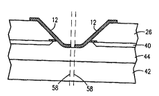
Fig. 13 illustrates at reference numeral 350, a
preferred cross sectional configuration of a notch 352
produced by partially cuttlng as described hereinabove in
connection with Fig. 4E. In contrast to the embodiment
illustrated in Fig. 6, where vertical lines 56 indicate
the intersection of the notch 54 with the pads 34, defin-
ing exposed sectional pad surfaces 51, in the present
emho~li ~nt, the notch 352 does not engage pads 354.
Fig. 14 illustrates a subses[uent manufacturing
step wherein a straight cut 356 is formed at the center
of notch 352 and exposes edges of pads 354.
Fig. 15 illustrates the formation of metal
contacts 358 along the inc~lined edges 360, part of the
top surface 362 and part of perpendicular side walls 364,
whlch extend perpendicularly to top surface 362. These
contacts, which may be formed by any suitable metal
deposition technique, are seen to extend inside notch 352
and inside straight cut 356, thus establishing electrical
contact with edge surfaces 366 of pads 354.
Here, the metal contacts are formed onto the
dies in electrical contact with surfaces 366 of pads 354
af ter separating the dies into indiYidual chips .
It will be apparent to persons skilled in the
art that the present inventio~ is not limited to what has
been particularly shown and described hereinabove. Rather
the scope of the present invention is defined only by the
claims which follow: