Note: Descriptions are shown in the official language in which they were submitted.
218I379
NONOLITHIC CRY8TAL 8TRIP FILTER
8PBCIFICATION
Technical Field:
The present invention relates to a monolithic filter
utilizing a strip of quartz crystal. The monolithic filter is
particularly useful in miniaturized electronic equipment where
low profile and minimum circuit board real estate are a concern.
Background:
A primary objective of electronics today is the
miniaturization of equipment while maximizing performance per
unit price. This objective is especially important in electronic
communications equipment where size and weight are a concern.
Cellular telephones and radios for aircraft and land vehicles are
but a few examples of devices wherein miniaturization is a major
objective. An important component in many communications devices
is a monolithic filter that allows a desired signal at a specific
frequency to pass into the electronic device while filtering out
unwanted signals.
2181379
Figures 1 and 2 illustrate a standard two-pole monolithic
crystal filter package containing a crystal blank, a base upon
which the crystal blank is mounted and a can or cover for
enclosing the crystal blank. As should be understood, the
crystal blank is relatively large and round and resembles the
shape of a circular-like disk. The crystal disk is mounted in a
substantially perpendicular orientation relative to the base so
that the resulting height dimension of the filter package is
greater than the diameter of the disk. Input and output
electrodes are formed near the center of one surface of the disk.
Ground electrodes are formed on an opposite surface of the disk
and are disposed in substantial registry with the input and
output electrodes. Ground and mounting contacts are formed at
specific locations along the perimeter of the disk. The
electrodes are electrically connected to the contacts by thin
"flags" formed on the surface of the disk. Commercially
available monolithic crystal disk filters are available in
multiple pole designs, such as two-pole, four-pole, six-pole,
eight-pole, etc.
Many factors must be taken into account when designing a
monolithic filter having a specific output signal performance.
Monolithic filters are typically designed to have an output
signal with a specific center frequency and bandwidth. The
filters are also designed to produce an output signal with
218137~
predetermined levels of ultimate attenuation, insertion loss
(loss of output signal strength) and spurious responses (unwanted
output signal responses). For example, electrical devices
operating on a principle of amplitude modulation (AM) require a
narrower bandwidth than devices operating on a principle of
frequency modulation (FM). Similarly, devices operating on FM
require a narrower bandwidth than devices operating on pulse
modulation (PM).
Bandwidth or bandpass is a function of electrode separation,
length of electrode and thickness of the crystal blank and plated
elements. The closer the electrodes are together, the wider the
bandwidth of the output signal. The thicker the crystal blank,
the lower the center frequency and the wider the bandwidth of the
output signal. Insertion losses are typically greater for output
signals with narrow bandwidths due to the increase in Q of the
circuit. Spurious responses are typically more active for output
signals with wide bandwidths. A more complete discussion of
crystal filter design can be found in the book entitled Crystal
Filters - Design, Manufacture, and Application authored by Robert
G. Kinsman and published by John Wiley & Sons, Inc. in 1987, the
substance of which is incorporated by reference herein.
The size and shape of the crystal blank are important
limitations when designing a miniaturized monolithic crystal
filter. The closer the electrodes are to the contacts or the
2181379
edges of the blank, the greater the insertion losses and spurious
responses will typically be. In standard crystal filter designs,
the electrodes are typically no closer to the edge of the blank
than ten times the thickness of the blank. As noted above, the
output signal bandwidth is also a function of the distance
between the input and output electrodes. The electrode pairs
must be spaced apart the most for low frequency, narrow bandwidth
filters. The size of the electrodes must also be taken into
consideration. The larger the area of the electrodes, typically
the lower the center frequency of the output signal. The longer
the electrodes, typically the narrower the bandwidth.
One problem with commercially available monolithic filter
designs is the size and shape of the crystal disk. The large
size and round shape of the disk contained in conventional
crystal filters is detrimental to the miniaturization of
electronic devices. This specific problem has become even more
pronounced in recent years given the trend in the electronics
industry to split a single circuit board containing a large
number of components into several separate circuit boards
containing a portion of the components. These separate circuit
boards are then stacked, one on top of the other, to effectuate
the miniaturization of the electronics devices. As should be
appreciated, the distance between the circuit boards is often
dictated by the height of the monolithic crystal filter.
2181379
Many attempts have been made to reduce the height of
monolithic filters. More specifically, the electronics industry
has attempted to install monolithic crystal disk filters in
ceramic chip carriers. However, even after substantial research
and capital expenditures, the amount of circuit board space or
real estate consumed by the ceramic chip carriers continues to be
too large. As should be understood, circuit board real estate is
the surface area of the circuit board consumed by a given
component, such as the monolithic filter and similar assemblies.
The combined cost of the ceramic chip carrier and the increase
in real estate consumed by the ceramic chip carrier more than
offsets the costs and benefits obtained by the reduction in
height for commercial production purposes.
The electronics industry also attempted to substitute
monolithic crystal disk filters with surface acoustic wave (SAW)
filters. However, SAW filters are proving to be unsuitable for
many purposes. For example, the center frequency of a standard
SAW filter drifts with changes in temperature. These filters are
generally used in applications experiencing a narrow temperature
range of between 20~C to 50~C. Commercial applications typically
require filter output stability between a larger range of
temperature -30~C to 70~C, and military applications require a
temperature stability between -40~C to 85~C.
2181379
The electronics industry has also attempted to reduce the
height of monolithic crystal disk filter packages themselves. As
best shown in Figure~ 1 and 2, these filter packages have input
and output posts or leads that project from the lower surface of
the base. These posts can be bent so that both the crystal disk
and the filter package lay flat against or parallel to the
circuit board. Unfortunately, these same designs are not readily
mountable to circuit boards, especially by conventional surface
mount pick-and-place machines which are widely employed in this
industry segment. Other designs have included a crystal disk
mounted in a substantially parallel orientation relative to the
filter base. An example of such a design is shown in United
States Patent No. 5,281,935, the disclosure of which is
incorporated by reference herein. The most noteworthy problem
associated with these designs, however, is that the monolithic
crystal disk filter packages take up a great deal of circuit
board real estate when the large crystal disk is positioned in a
substantially parallel orientation relative to the circuit board.
Again, the costs and associate benefits of the reduction in
filter height is viewed as being offset by the costs attendant to
the increase in real estate consumed by the individual filters.
Other attempts in the art were made to modify commercially
available end mounted, discrete crystal strip resonators
illustrated in Figure~ 3 and 4 to produce an end mounted,
2181379
monolithic crystal strip filter shown in Figures 5 and 6.
Although commercially unsuccessful, these end mounted or tubular
monolithic filters would have reduce the real estate consumed by
the base of the filter when mounted in an upright orientation on
the circuit board. Unfortunately, while commercially acceptable
discrete crystal strip resonators are available in both end
mounted designs similar to that shown in Figure~ 3 and 4 and low
profile designs similar to that illustrated in Figure 7, to date,
no monolithic crystal strip filter exists in either an end
mounted or low profile designs.
Another problem encountered with miniaturized monolithic
crystal filters is the amount of spurious responses and insertion
loses which are associated with the output signal. One reason
for increases in spurious responses and insertion loses is
believed to be the close placement of the electrodes relative to
the mounting and ground contacts as a result of the reduced size
of the crystal blank. As should be understood, small crystal
blanks simply do not provide a great deal of surface area within
which to position various components when designing specific
monolithic filters which are intended for particular
applications.
A further problem faced by the electronics industry is
maintaining a competitive price for miniaturized crystal filters.
This requires particular attention to the costs associated with
2181379
manufacturing the individual miniaturized filters. To minimize
manufacturing expenses, monolithic crystal filter designs should
utilize standard bases, such as HC-45, HC-49 or UM-l base
designs. The miniaturized filter should further be mountable on
the base without extensive modification of the base or to the
machines employed to manufacture the base. Filter designs that
require substantial retooling of these manufacturing machines
prior to commercial production result in dramatic increases in
the cost of the miniaturized filters which normally renders the
filters impractical for commercial purposes.
A still further problem faced by the electronics industry is
that miniaturized crystal filters should be adapted for
installation on existing circuit boards without significant
redesign of the component layout of the circuit boards. As would
be expected, modifications to the existing circuit board designs
can dramatically increase the cost of employing the miniaturized
filter, and thus the cost of the electronic devices utilizing the
filter.
The present invention is provided to solve these and other
problems.
Summary of the Invention:
The present invention relates to a low profile monolithic
crystal strip filter and filter package. More specifically, the
218I379
filter includes an AT-cut rectangular strip of quartz crystal
having a length of about 1/3 to 1/4 of an inch; a width of about
1/10 to 1/20 of an inch; and a thickness of about S/10,000 to
100/10,000 of an inch. The filter includes input, output, and
ground electrodes formed symmetrically on the strip. Each
electrode is connected to its respective mounting or ground
contact by means of flag. The electrodes, contacts and flags
have a predetermined size and shape, and are arranged in a
predetermined configuration on the crystal strip to minimize
spurious responses and insertion losses. The crystal strip is
mounted to an HC-45 or HC-49 base to minimize production costs.
A low profile can or cover forms a hermetic seal with the base,
thereby enclosing the crystal strip. A ground wire connects the
filter ground contact to the base. A ground post projects from a
lower surface of the base. The filter can take the form of a
two-pole design with a single set of input, output and ground
electrodes located symmetrically upon the crystal strip; or a
four-pole design with two sets of input, output and ground
electrodes located symmetrically on the crystal strip. The
output signal has a center frequency of about 4 to 500 MHz, a 3
dB bandwidth of about 3 to 250 kHz, an ultimate of normally
better than 60 dB, st~n~rd insertion losses for the number of
poles in the filter and commercially viable spurious responses.
2181379
-
A major advantage of the present monolithic crystal strip
filter invention is that it dramatically reduces the height of
commercially available monolithic crystal filter packages without
substantially increasing the circuit board real estate consumed
by the filter packages. For example, the height of a monolithic
crystal filter utilizing a stAn~Ard HC-45 or UM-l base design is
reduced from about 0.30 inches to about 0.15 inches, or
approximately one-half the original height. The height of a
filter utilizing a standard HC-49 filter design is reduced from
about 0.45 inches to about O.lS inches, or approximately one-
third the height. This low profile design with reduced height
enables the circuit boards in electronics devices to be stacked
significantly closer together, thereby reducing the overall size
and weight of the resulting electronic device employing the
filter.
An additional advantage of the present invention is that the
relatively small monolithic crystal strip filter produces an
output signal having a thermally stable center frequency with a 3
dB bandwidth of about 3 to 250 kHz through center frequencies of
about 4 to 500 MHz. The filter also produces standard insertion
losses for the number of poles in the filter and spurious
responses which are commercially acceptable. This performance is
achieved despite the fact that the electrodes have a width of
about one-half the width of the strip, and are positioned within
2181379
distances in the range of five to ten times the thickness of the
blank when measured from the edges of the blank. This
performance is also achieved despite the fact that the ground
contacts are positioned about 0.02 inches from the electrodes,
and about 30 to 40 percent of the entire surface of the strip is
plated or metalized with electrodes, contacts and flags.
A further advantage of the present invention is that most of
the machinery used to manufacture discrete crystal strip
resonators can be employed effectively to manufacture the present
monolithic crystal strip filter invention in a low profile
package. For example, a conventional pick-and-place machine can
be used to install the crystal strip filter to the mounting posts
of the base.
A still further advantage of the present monolithic crystal
strip filter is that it may be installed on an existing HC-45,
HC-49 or UM-l base without requiring the redesign of the base or
modification of the equipment employed to install the crystal
strip filter on the base. As earlier discussed, the use of the
HC-45, HC-49 or UM-l bases dramatically reduces the costs which
are attributable to retooling production equipment, and therefore
reduces the manufacturing expenses related to miniaturized
monolithic crystal filters.
A still further advantage of the present invention is that
the low profile design enables the lower surface of the base to
2181379
be mounted in substantially parallel relation to an associated
circuit board. This mounting orientation is very important from
a commercial standpoint because the respective filters can be
readily installed on a circuit board by again utilizing a
S conventional pick-and-place machine after the individual posts of
the base are bent or otherwise deformed for surface mounting
applications. As should be understood, the use of pick-and-place
machines permits rapid, automated, and cost efficient
installation of the filter package to an associated circuit
board.
A still further advantage of the present invention is that
it provides a monolithic crystal strip filter that can be
installed in current circuit board designs without significant
redesign of the circuit board component layout. This, of course,
reduces the costs attendant to incorporating the invention into
existing electronics devices and further reduces the final cost
of the miniaturized electronic device.
Other features and advantages of the present invention will
become readily apparent from the following specification, taken
in combination with the following drawings.
Brief DescriPtion of Drawinqs:
Figure 1 is a perspective, enlarged, exploded, front
elevation view of a standard two-pole monolithic crystal disk
218137~
filter which is mounted on an HC-49 base and which has a standard
height can.
Figure 2 is a perspective, enlarged, rear elevation view of
the monolithic crystal disk filter of Figure 1.
Figure 3 is a perspective, enlarged, exploded, front
elevation view of a standard end mounted discrete crystal strip
resonator, and which is mounted on a glass base and includes a
tubular can.
Figure 4 is a perspective, enlarged, rear perspective view
of the discrete crystal strip resonator of Figure 3.
Figure 5 is a perspective, enlarged, exploded, front
elevation view of an earlier attempt to manufacture an end
mounted, monolithic crystal strip filter, and which is mounted on
a glass base and includes a tubular can.
lS Figure 6 is a perspective, enlarged, rear elevation view of
the monolithic crystal strip filter of Figure 5.
Figure 7 is a perspective, enlarged, exploded, plan view of
a standard, low profile discrete crystal strip resonator mounted
on the HC-49 base and which employs a low profile can.
Figure 8 is an enlarged exploded, plan view of the present
low profile, two-pole monolithic crystal strip filter package
invention.
Figure 9 is an enlarged, exploded, side sectional view of a
first embodiment of the two-pole, monolithic crystal strip filter
13
2181373
invention mounted on the prior art HC-49 low profile base and
having a low profile can.
Figure 10 is an enlarged, top plan view of the two-pole
monolithic crystal strip filter of Figure 9.
Figure 11 is an enlarged top plan view of the two-pole
monolithic crystal strip of Figure 9 showing the placement of the
signal electrodes, flags and mounting and ground contacts.
Figure 12 is an enlarged bottom view of the two-pole,
monolithic crystal filter of Figure 9 showing the placement of
the ground electrode, flags and mounting and ground contacts.
Figure 13 is a graphical representation of a sample output
signal for the two-pole filter of Figures 9-12.
Figure 14 is a plot of a sample output signal for two two-
pole filters of Figures 9-12 connected in series.
figure 15 is an enlarged exploded side sectional view of a
second embodiment of the two-pole, monolithic crystal filter
invention mounted on an HC-45 low profile base and having a low
profile can.
Figure 16 is a top view of the two-pole, monolithic crystal
strip filter of Figure 15.
Figure 17 is a top view of the two-pole monolithic crystal
strip filter of Figure 15 showing the placement of the signal
electrodes, flags and mounting and ground contacts.
14
2181379
Figure 18 is a bottom view of the two-pole, monolithic
crystal strip filter of Figure 15 showing the placement of the
ground electrode, flags and mounting and ground contacts.
Figure 19 is an enlarged exploded side sectional view of the
present low profile, four-pole monolithic crystal strip filter
package invention.
Figure 20 is an enlarged exploded perspective view of a
first embodiment of the present four-pole monolithic crystal
strip filter invention mounted on the HC-49 low profile base and
having a low profile can.
Figure 21 is a top view of the four-pole monolithic crystal
strip filter of Figure 20.
Figure 22 is a top view of the four-pole monolithic crystal
strip filter of Figure 20 showing the placement of the signal
electrodes, flags, ground shield and mounting and ground
contacts.
Figure 23 is a bottom view of the four-pole monolithic
crystal strip filter of Figure 20 showing the placement of the
ground electrode, flags, ground shield and mounting and ground
contacts.
Figure 24 is a geographical representation of a sample
output signal for the four-pole filter of Figures 20-23.
Figure 25 is an enlarged exploded side sectional view of a
second embodiment of the present four-pole monolithic crystal
2181379
filter invention mounted on the HC-45 low profile base and having
a low profile can.
Figure 26 is a top view of the four-pole monolithic crystal
strip filter of Figure 25.
Figure 27 is a top view of the four-pole monolithic crystal
strip filter of Figure 25 showing the placement of the signal
electrodes, flags, ground shield and mounting and ground
contacts.
Figure 28 is a bottom plan view of the four-pole monolithic
crystal strip filter of Figure 25 showing the placement of the
ground electrode, flags, ground shield and mounting and ground
contacts.
Figure 29 is an enlarged side view of the present filter
package invention showing the mounting and ground posts bent for
surface mount applications.
Figure 30 is a bottom view of the filter package of Figure
29.
Figure 31 is an enlarged plan view showing two low profile,
two pole monolithic crystal strip filters connected in series.
Detailed Description:
While this invention is susceptible of embodiments in many
different forms, there is shown in the drawings and will herein
after be described, several forms of the invention with the
16
218I379
understanding that the present disclosure is to be considered as
an exemplification of the principles of the invention, and is not
intended to limit the broad aspects of the invention to the
several embodiments illustrated.
The present invention relates to a low profile monolithic
crystal strip filter package which is generally designated by the
numeral 10; and a monolithic crystal strip filter which is
generally designated by the numerals 100, 200, 300 and 500,
respectively, and which may be mounted in the package 10. As
should be understood, Figures 8-12 illustrate the two-pole strip
filter 100 mounted on a st~ rd HC-49 through-hole base; Figure
13 and 14 show plots of sample output signals responses produced
by this two-pole filter; Figure~ 15-18 show the two-pole strip
filter 200 mounted on a st~n~rd HC-45 through-hole base; Figure~
19-23 show the four-pole strip filter 300 mounted on the HC-49
through-hole base; Figure 24 shows a sample output signal
response produced by this four-pole filter; and Figures 25-28
show the four-pole strip filter 500 mounted on the HC-45 base.
Each of these forms of the invention is discussed in greater
detail below.
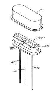
As best seen in Figure 9 and 10, the filter package 10
includes a housing 15 formed by a base 20 and a low profile can
70. The base 20 includes a main body 21 that is relatively long
in comparison to its width. The main body 21 has an upper
2I81379
surface 22 and a lower surface 23. The main body 21 also has
first and second ends 24 and 25 and first and second sides 26 and
27 that define its perimeter 28. The base 20 includes a flange
30 that projects outwardly relative to the perimeter 28. The
flange 29 is oriented in substantial flush relation with the
lower surface 23 of base 20, and thereby creates a surface for
matingly engaging the can 70 as will be discussed later. The
base 20 is preferably manufactured from an electrically
conductive and ferrous metal and is coated with a corrosion
resistant nickel coating. This is similar to the standard,
commercially available HC-45 or HC-49 base designs which are
manufactured pursuant to United States Military Specification No.
MIL-H-10056. It should be understood that individual filters 100
and 300 could be installed on a base equivalent to the HC-49
base, and that filters 200 and 500 could be installed on a base
equivalent to the HC-45 base, an example of an equivalent HC-45
base is the UM-l base.
The main body 21 of the base 20 contains a pair of openings
located substantially midway between its sides 26 and 27. Each
of the respective openings individually matingly receives an
electrical insulator 31 or 32, such as the glass insulators as
employed in the HC-45 or HC-49 base designs. Insulator 31
matingly receives an input mounting post 40, and insulator 32
matingly receives an output mounting post 50. A ground post 60
18
2181379
is welded to the lower surface 23 of base 20 at a location
substantially midway between mounting posts 40 and 50. A lower
portion 41 of input post 40 and a lower portion 51 of output post
50 are aligned in substantially parallel orientation to ground
post 60. Posts 40, 50 and 60 project substantially
perpendicularly outwardly from the lower surface 23 of base 20,
and are electrically conductive and preferably made of kovar with
a tin plating as in HC-45 and HC-49 base designs.
Each of the mounting-posts 40 and 50 has an upper portion 42
or 52. The upper portions 42 and 52 are substantially flat and
are bent or otherwise deformed in a predetermined step-like
fashion. As best seen in Figure 9, the upper portion 42 is bent
toward the base end 24 so that its end 44 is located inside base
end 24. Upper portion 52 is bent toward the base end 25 so that
its end 54 is located inside the base end 25.
The low profile can 70 matingly interfits with the base 20
to form the hermeticly sealed housing 15 that contains the
individual monolithic crystal strip filters 100, 200, 300 or 500.
The can 70 has individual side walls 71-74 that define the inside
of the can. The can 70 is closed at one end by an end wall 75,
and is open at its opposite end 76. The open end 76 of can 70 is
shaped to matingly engage or interfit with the upper surface of
the flange 29 to form a hermetic seal which encloses the
respective monolithic strip filter 100, 200, 300 or 500. Side
19
218I379
walls 71-74 have a predetermined height dimension which prevents
end wall 75 from physically contacting the individual monolithic
strip filters 100, 200, 300 or 500 or post ends 44 and 54.
As earlier discussed, Figures 9-12 illustrate a first form
of a low profile two-pole monolithic crystal strip filter 100
which contains a piezoelectric AT-cut quartz crystal strip 110.
The crystal strip 110 is substantially rectangular in shape, and
further has substantially parallel, upper or first surface 112
and lower or second surface 113. The crystal strip 110 has first
and second ends 114 and 115, and first and second sides 116 and
117, that define an outer perimeter or periphery 118. Each end
114 and 115 of the strip 110 is mounted on the upper most step of
its respective post 40 or 50. The strip 110 is further oriented
or aligned in substantially parallel relation to the upper
surface 22 of the base 20. The strip 110 is substantially
centered or positioned over the upper surface 22 of the base 20,
and the perimeter 118 of the strip is located within the
perimeter 28 of the surface 22 such that the edges 114-117 of the
strip do not physically engage the individual side walls 71-74 of
the can 70. In this form of the invention, the length dimension
of the strip 110 is roughly three times greater than its width
dimension. The crystal strip 110 preferably has a length
dimension of about 0.320 inches and a width dimension of about
2181379
0.102 inches to facilitate installation of the filter on the
associated HC-49 base.
As best seen in Figures 11 and 12, the crystal strip 110 has
a center line 120 which extends from one end 114 of the strip to
the other 115. The center line 120 is located approximately
midway between the sides 116 and 117 of the crystal strip, and
thereby divides the crystal strip 110 into substantially equal
halves. The crystal strip 110 also includes a dividing line, or
line of symmetry 130 which extends from one side 116 of the strip
to the other 117. The line of symmetry 130 is located
approximately midway between the individual ends 114 and 115, and
thereby divides the crystal strip 110 into two substantially
equal portions 131 and 132.
The monolithic filter 110 includes one set of input and
output or signal electrodes 141 and 151 which are individually
formed on the upper surface 112 of the crystal strip 110. This
is best illustrated by reference to Figure 11. The individual
input and output electrodes 141 and 151 are substantially the
same size and shape, and further have respective length and width
dimensions of about 0.050 inches each. Each of the electrodes
141 and 151 is oriented in a predetermined location on center
line 120 and located a given distance of about 0.002 inches from
the line of symmetry 130. Electrode 141 is electrically
connected to a mounting contact 142 located on one end 114 of the
218137~
strip by a flag 145. Electrode 151 is electrically connected to
a mounting contact 152 located on the other end 115 of the strip
by a flag 155.
Mounting contact 142 has a portion 143 formed on the upper
surface 112 of the strip and a portion 144 formed on the lower
surface 113. Similarly, mounting contact 152 has a portion 153
formed on the upper surface 112 of the strip and a portion 154
formed on lower surface 113. The lower portions 143 and 153 are
aligned in substantial registry with their respective upper
portions 144 or 154. Each of the upper mounting contact portions
143 or 153 is electrically coupled to its respective lower
mounting contact portion 144 or 154 by electrically conductive
cement applied when securing the filter 100 to the mounting posts
40 and 50. Each of the respective mounting contact portions 143,
lS 144, 153 and 154 is substantially the same size and shape, and
has a given length of about 0.040 inches and width of about 0.050
inches. The individual mounting contacts 142 and 152, are
substantially symmetrically oriented about center line 120, and
are further located at locations proximal the strip ends 114 or
115, respectively. Mounting contacts 142 and 152 have a width
substantially the same as electrodes 141 and 151. The individual
flags 145 and 155 are substantially the same size and shape, with
a given length dimension of about 0.068 inches and a given width
dimension of about 0.015 inches.
22
2181379
A pair of ground electrodes 161 and 171 are formed on the
lower surface 113 of the crystal strip 110, as shown in Figure
12. Each of the ground electrodes 161 and 171 is electrically
coupled to a ground contact 165 by means of a ground flag 162 or
172. The ground electrodes 161 and 171 are substantially the
same size and shape and are aligned in substantial registry with
the input and output electrodes 141 and 151, respectively. Each
of the ground electrodes 161 or 171 also includes a symmetry flag
163 or 173, respectively. The individual symmetry flags 163 and
173 are substantially the same size and shape and are aligned in
substantial registry with the individual flags 145 or 155,
respectively. The symmetry flags 163 and 173 are shorter than
the individual flags 145 and 155 and do not physically contact
the lower portions 144 and 154 of the individual mounting
contacts 142 and 152. The ground electrodes 161 and 171 and the
symmetry flags 163 and 173 are positioned substantially
symmetrically about center line 120. The ground electrodes 161
and 171; the flags 162 and 172; and the symmetry flags 163 and
173 are also located substantially symmetrically about line~130.
Although the ground electrodes 161 and 171 have been shown and
described as being two separate electrodes, it should be
understood that they could be joined to form a single ground
electrode which is oriented in substantial registry with both the
input and output electrodes 141 and 151.
23
218137~
Ground contact 165 has a portion 166 formed on upper surface
112 of the strip and a portion 167 formed on lower surface 113.
Lower portions 167 is aligned in substantial registry with upper
portions 166. Upper ground contact portion 166 is electrically
connected to its lower ground contact portion 167 by electrically
conductive cement applied when securing the ground member which
is preferably a wire 180 to the filter 100. Ground contact 165
is substantially centered about line of symmetry 130 and is
located proximal strip side 116.
The individual electrodes 141, 151, 161 and 171; contacts
142, 152 and 165, and the flags 145, 155, 162, 163, 172 and 173
are conductive elements which are arranged in a predetermined
configuration on the surfaces 112 and 113 of the crystal strip
110 to produce a commercially viable two-pole filter. The
specific configuration of the plated elements can be defined by
designating side 116 or center line 120 as an x-axis and end 114
as a y-axis, and describing the position of each element in
relation to these axes. The x-axis extends from one end 115 of
the strip to the other or from 0.0 to 1Ø Similarly, the y-axis
extends from one side 116 of the strip to the other 117 or from
0.0 to 1Ø As should be understood, the individual elements are
arranged on the upper and lower surfaces 112 and 113 of the
crystal strip 110 in roughly the following configurations:
24
2181379
.
Configuration of Two-Pole StriP Filter 100
PLATED ELEMENT X-AXIS Y-AXIS
Upper 8urface 112
Mounting Contact 1430.00 to 0.13 0.25 to 0.75
Electrode Flag 1450.13 to 0.34 0.43 to 0.57
Electrode 141 0.34 to 0.49 0.25 to 0.75
Electrode 151 0.51 to 0.66 0.25 to 0.75
Electrode Flag 1550.66 to 0.87 0.43 to 0.57
Mounting Contact 1530.87 to 1.00 0.25 to 0.75
Ground Contact 1660.40 to 0.60 o.00 to 0.06
Lower ~urface 113
Mounting Contact 1440.00 to 0.13 0.25 to 0.75
Symmetry Flag 1630.19 to 0.34 0.43 to 0.57
Ground Electrode 1610.34 to 0.49 0.25 to 0.75
Ground Electrode 1710.51 to 0.66 0.25 to 0.75
Symmetry Flag 1730.66 to 0.81 0.43 to 0.57
Mounting Contact 1540.87 to 1.00 0.25 to 0.75
Ground Contact 1670.42 to 0.58 0.00 to 0.06
Ground Flag 1620.42 to 0.45 0.06 to 0.25
Ground Flag 1720.55 to 0.58 0.06 to 0.25
Figure 13 illustrated a graphical depiction of a sample
output signal produced by crystal filter 100 when the above
elements are plated onto the crystal strip 110 in the above
configuration and to the approximate dimensions shown in Figures
11 and 12. To achieve a center frequency of about 21.4 MHz,
strip 110 should have a thickness of about 0.003000 inches and
the plated elements should have a thickness of about 0.000028037
inches on each side of the strip. Other center frequencies
between the range of about 4 to 500 MHz should be obtainable by
varying the thickness of the strip and plated elements. Other
bandwidths between the range of 3 to 250 kHz should be obtainable
218I379
-
by varying the electrode separation, length of the electrodes and
thickness of the strip and plated elements.
The depiction shown in Figure 13 is for a constant 0.419 dBm
input signal through a frequency span of 600 kHz. The crystal
filter 100 produces a 3 dB bandwidth of about 30 kHz, a 15 dB
bandwidth of about 80 kHz and a potential 30 dB bandwidth of
about 200 kHz. The crystal filter 100, has an insertion loss of
about 1.2 dB. For the sample filter graphically depicted in
Figure 13, the spurious responses occur at high side frequency
offsets of about 110 kHz to a level of about 6 dB; 170 kHz to a
level of about 12 dB: and 250 kHz to a level of about 4 dB. The
filter 100 has a low side ultimate attenuation of about 55 dB and
a high side ultimate of about 55 dB. It should be understood
that the output signal will vary somewhat for each filter made to
the above configuration and dimensions due to manufacturing
tolerances.
Figure 14 shows a plot of a sample output signal produced by
two filter packages 10 placed in series, each package containing
one filter 100. The plot is for a constant 0.429 d8m input
signal through a frequency span of 600 kHz. The two combined
filters 100 produce an output signal with a 3 dB bandwidth of
about 30 kHz; a 15 dB waveband of about 50 kHz; and a 30 dB
bandwidth of about 70 kHz; and a potential 60 dB bandwidth of
about 160 kHz. The two crystal filters 100, which are
26
218I379
electrically coupled in series, have a combined insertion loss of
about 1.8 dB. Spurious responses occur at frequency offsets of
about approximately 108 kHz to a level of about 25 dB; 160 kHz to
a level of approximately i5 dB; and 250 kHz to a level of
approximately 31 dB. These spurious responses are believed to be
commercially acceptable for a wide range of applications. The
filter 100 has a low side ultimate of about 90 dB and a high side
ultimate of about 90 dB.
Figures 15-18 illustrate a second form of the low profile
two-pole monolithic crystal strip filter 200. This form of
invention includes a piezoelectric AT-cut quartz crystal strip
210. The crystal strip 210 is substantially rectangular in shape
and has substantially parallel, upper or first surface 212 and
lower or second surface 213. The crystal strip 210 has first and
second ends 214 and 215, and further has first and second sides
216 and 217, respectfully, that define an outer perpendicular
perimeter 118. Each end 214 and 215 of the strip 210 is mounted
on the upper most step of its respective post 40 or 50. The
crystal strip 210 is aligned or otherwise oriented in
substantially parallel relative relation to the surface 22 of the
base 20. The crystal strip 210 is substantially centered or
otherwise oriented in a predetermined position on the surface 22
of base 20. The perimeter 218 of the strip is within the
perimeter 28 of surface 22 such that the edges 214-217 of the
2181379
strip do not physically engage the individual side walls 71-74 of
the can 70. In this form of the invention, the length dimension
of the strip 210 is roughly four times greater than its width
dimension. The crystal strip 210 prefera~ly has a length
dimension of about 0.229 inches and a width dimension of about
0.052 inches to facilitate mounting on the HC-45 base.
The crystal strip 210 has a center line which is designated
by the numeral 220 which extends from one end 214 of the crystal
strip to the opposite end 215. The center line 220 is located
about midway between the sides 216 and 217 of the crystal strip
and divides the crystal strip 210 into substantially equal
halves. The crystal strip 210 also includes a dividing line or
line of symmetry which is distinguished by the numeral 230 and
which extends from one side 216 of the strip to the other side
217. The line of symmetry 230 is located approximately midway
between the respective ends 214 and 215, and divides the strip
210 into two substantially equal portions 231 and 232,
respectively.
The monolithic filter 110 includes one set of input and
output or signal electrodes 241 and 251, respectively, which are
formed on the upper surface 212 of the crystal strip 210. This
is best seen by reference to Figure 17. The input and output
electrodes 241 and 251 are substantially the same size and shape,
and have a length dimension of about 0.020 inches, and a width
28
218I379
dimension of about 0.027 inches. Each of the electrodes 241 and
251 is oriented substantially symmetrically about the center line
220 and further located a given distance of about 0.002 inches
from the line of symmetry 230. Electrode 241 is electrically
coupled to a mounting contact 242 by an electrode flag 245.
Electrode 25 is electrically connected to a mounting contact 25
by a similar electrode flag 255.
Mounting contact 242 has a portion 243 formed on upper
surface 212 of the strip and a portion 244 formed on lower
surface 213. Mounting contact 252 has a portion 253 formed on
upper surface 212 of the strip and a portion 254 formed on the
lower surface 213. The individual lower portions 243 and 253 are
aligned in substantial registry with the corresponding upper
portions 244 and 254, respectively. Each of the respective upper
mounting contact portions 243 or 253 is electrically coupled with
its corresponding lower mounting contact portion 244 or 254 by
electrically conductive cement. Each of the respective mounting
contact portions 243, 244, 253 and 254 is substantially the same
size and shape, and further has a length dimension of about~0.033
inches and a width dimension of about 0.027 inches. The mounting
contacts 242 and 2S2 are oriented in predetermined location about
the center line 220 and are located proximal strip ends 214 or
215, respectively. The mounting contacts 242 and 252 have a
width substantially the same as electrodes 241 and 251. The
29
2181~79
-
flags 245 and 255 have substantially the same size and shape, and
further have a length dimension of about 0.060 inches and a width
dimension of about 0.015 inches.
A pair of ground electrodes 261 and 271 are formed on the
lower surface 213 of crystal strip 210 as shown in Figure 18.
Each of the ground electrodes 261 and 271 is electrically
connected to a corresponding ground contact 265 by means of a
ground flag 262 or 272. The ground electrodes 261 and 271 are
substantially the same size and shape and aligned in spaced,
substantially parallel registry with the input and output
electrodes 241 and 251, respectively. Each of the ground
electrodes 261 or 271 includes a symmetry flag which is
identified by the numerals 263 or 273, respectfully. The
individual symmetry flags 263 and 273 are substantially the same
size and shape as the respective input and output electrode flags
245 and 255 and are further aligned in substantial registry with
the individual input and output electrode flags 245 or 255,
respectively. The symmetry flags 263 and 273 are shorter in
relative comparison than the input and ou~u~ electrode flags 245
and 255 and do not contact the lower portions 244 and 254 of the
individual mounting contacts 242 or 252. The ground electrodes
261 and 271 and their respective symmetry flags 263 and 273 are
positioned in a substantial symmetrically orientation about the
center line 220. The ground electrodes 261 and 271; ground flags
2181379
262 and 272 and symmetry flags 263 and 273 are also located in a
substantial symmetrical orientation about the line of symmetry
230. Although the ground electrodes 261 and 271 have been shown
and described as being two separate electrodes, it should be
understood that they could be joined in a fashion to form a
single ground electrode which is disposed in substantial
registry with both the input and output electrodes 241 and 251.
Ground contact 265 has a portion 266 formed on upper surface
212 of the strip and a portion 267 formed on lower surface 213.
Lower portions 267 is aligned in substantial registry with upper
portions 266. Upper ground contact portion 266 is electrically
connected to its lower ground contact portion 267 by electrically
conductive cement applied when securing the ground member which
is preferably a wire 280 to the filter 200. Ground contact 265
is substantially centered on line of symmetry 230 and is located
proximal strip side 216.
The individual electrodes 241, 251, 261 and 271; the
respective contacts 242, 252 and 265, and the individual flags
245, 255, 262, 263, 272 and 273 form a series of elements which
are arranged in a predetermined configuration or pattern on the
individual surfaces, 212 and 213 of the crystal strip. These
patterns or configurations produce a commercially viable two-pole
crystal filter having a minimum amount of spurious responses and
insertion losses. The elements are arranged on the upper and
2I81379
-
lower surfaces 112 and 113 of the crystal strip 110 in roughly
the following configurations:
Confiquration of Two-Pole StriP Filter 200
ELEMENT X-AXIS Y-AXIS
Upper 8urface 212
Mounting Contact 243 0.00 to 0.14 0.24 to 0.76
Electrode Flag 2450.14 to 0.40 0.36 to 0.64
Electrode 241 0.40 to 0.49 0.24 to 0.76
Electrode 251 0.51 to 0.60 0.24 to 0.76
Electrode Flag 2550.60 to 0.86 0.36 to 0.64
Mounting Contact 253 0.86 to 0.10 0.24 to 0.76
Ground Contact 2660.45 to 0.55 0.00 to 0.12
Lower Surface 213
Mounting Contact 244 0.00 to 0.14 0.24 to 0.76
Symmetry Flag 2630.23 to 0.40 0.36 to 0.64
Ground Electrode 261 0.40 to 0.49 0.24 to 0.76
Ground Electrode 271 0.51 to 0.60 0.24 to 0.76
Symmetry Flag 2730.60 to 0.77 0.36 to 0.64
Mounting Contact 254 0.86 to 0.10 0.24 to 0.76
Ground Contact 2670.45 to 0.55 0.00 to 0.12
Ground Flag 2620.45 to 0.48 0.12 to 0.24
Ground Flag 2720.52 to 0.55 0.12 to 0.24
To achieve a center frequency of about 21.4 MHz, strip 110
should have a thickness of about 0.003000 inches and the plated
elements should have a thickness of about 0.000028037 inches on
each side of the strip. Crystal filter 200 achieves an output
signal performance similar to that which was earlier discussed
with respect to crystal filter 100. Again, different center
frequencies and bandwidths should be obtainable between the
ranges of 4 to 500 MHz and 3 to 250 kHz, respectively, by varying
32
2181379
the thickness of the strip and plated elements, and the
separation between and length of the electrodes.
Figures 19-23 illustrate a third form of the invention that
as a low profile four-pole monolithic crystal strip filter 300.
The crystal strip filter includes a piezoelectric AT-cut quartz
crystal strip 310. The crystal strip 310 is substantially
rectangular in shape with substantially parallel upper or first
surface 312 and lower or second surface 313. Crystal strip 310
has first and second ends 314 and 315, and first and second sides
316 and 317, that define an outer perimeter 318. Each end 314
and 315 of crystal strip 310 is mounted on the upper most step of
its respective post 40 or S0. The crystal strip 310 is oriented
or otherwise aligned substantially parallel to the surface 22 of
base 20. The crystal strip 310 is substantially centered or
otherwise oriented in a predetermined location on the surface 22
of base 20 so that the perimeter 218 of the strip is located
within the perimeter 28 of the base 20, and the edges 314-317 of
the crystal strip do not physically engage any of the side walls
71-74 of the can 70. The length dimension of the crystal strip
310 is roughly three times greater than its width dimension. The
crystal strip 310 preferably has a length dimension of about
0.320 inches and a width dimension of about 0.102 inches. These
physical dimensions facilitate the mounting on the HC-49 base.
2181~79
The crystal strip 310 has a center line 320 which extends
from one end 314 of the crystal strip to the opposite end 315.
The center line 320 is located about midway between the sides 316
and 317 of the crystal strip and divides the strip 310 into
substantially equal halves. The crystal strip 310 also includes
a dividing line or line of symmetry 330 which extends from one
side 316 of the crystal strip to the opposite side 317. The line
of symmetry 330 is located about midway between the individual
ends 314 and 315, respectively, and thereby divides the crystal
strip 310 into two substantially equal portions 331 and 332.
The four-pole monolithic filter 300 includes two sets of
signal electrodes 340 and 360. The first set of electrodes 340
includes an input electrode 341 an output electrode 351 and a
ground electrode 381. The second set of electrodes 360 includes
an input electrode 361 output electrode 371 and a ground
electrode 391. As best shown in Figure 22, the input and output
electrodes 341, 351, 361 and 371 are formed or otherwise borne by
the upper surface 312 of the crystal strip 310. These electrodes
are of substantially the same size and shape, and are oriented in
predetermined locations about the center line 320. Each of the
individual electrodes 341, 351, 361 and 371 has a length
dimension of about 0.033 inches, and a width dimension of about
0.043 inches. The individual electrodes 341 and 351 are spaced
about 0.004 inches apart. Electrodes 361 and 371 are also spaced
34
2181379
.,
the same distance apart. The first and second sets of electrodes
340 and 350 are located in a predetermined symmetrical pattern
about line of symmetry 330. The output and input electrodes 351
and 361 are electrically joined or coupled by a connection flag
352 which has a given width dimension of about 0.015 inches. The
connecting flag 352 has a first portion 353 which extends at
about a 45~ angle relative to the side 317 of crystal strip 310;
a second portion 354 which extends in an orientation which is
substantially parallel to, and along side 317; and a third
portion 355 which extends at a 45~ angle relative to the input
electrode 361. The input and output electrodes 341 and 371 are
electrically connected or coupled to a mounting contact 342 or
352 by flags 345 or 375, respectively.
The mounting contact 342 has a portion 343 formed on upper
lS surface 312 and a portion 344 formed on lower surface 313. The
mounting contact 372 has a portion 373 formed on upper surface
312; and a portion 374 formed on lower surface 313. The lower
portions 343 and 373 are aligned in substantial registry with
upper portions 344 and 374, respectively. The upper portions 343
or 373 of each of the mounting contacts is electrically connected
or coupled to its respective lower portion 344 or 374 by
electrically conductive cement. Further, each of the mounting
contact portions 343, 344, 373 and 374 is substantially the same
size and shape, and further has a length dimension of about 0.025
2181379
. ~ .
inches and a width dimension of about 0.043 inches. The mounting
contacts 342 and 372 are oriented in a pattern about the center
line 320 and otherwise positioned at their respective ends 314 or
315 of crystal strip 310. The mounting contacts 342 and 272 have
a width substantially the same as electrodes 341 and 371. The
flags 345 and 375 are substantially the same size and shape, and
further have with a length dimension of about 0.068 inches, and a
width dimension of about 0.015 inches. Each of the flags 345 and
375 extends from its respective electrode 341 or 371 to its
respective mounting contact 342 or 372.
Ground electrodes 381 and 391 are formed or otherwise borne
on the lower surface 313 of crystal strip 310. This is best
shown by reference to Figure 23. Each of the ground electrodes
381 and 391 is electrically connected or coupled to a ground
contact 400 by means of a ground flag 382 or 392, respectively.
The ground electrodes 381 and 391 have substantially the same
size and shape. Further, each of the ground electrodes 381 and
391 is also substantially aligned and otherwise disposed in
registry with its corresponding set of input and output
electrodes 340 and 360. Each of the ground electrodes 381 or 391
includes a symmetry flag 383 or 393. The individual symmetry
flags 383 and 393 have sizes and shapes that are substantially
equivalent to their respective input and output electrode flags
345 and 375. The symmetry flags are aligned or otherwise
36
2181379
disposed in substantial registry with the respective input and
output electrode flags. The symmetry flags 383 and 393 are
shorter, in relative comparison to the input and output electrode
flags 345 and 375 and do not physically contact the lower portion
344 and 354 of mounting contacts 342 or 352, respectively. The
ground electrodes 381 and 391 and their respective symmetry flags
383 and 393 are oriented or otherwise positioned in a symmetrical
pattern about the center line 320. The ground electrodes 381 and
391; the ground flags 382 and 392; and the pattern symmetry flags
383 and 393 are also located in a symmetrical pattern about the
line of symmetry 330. Although each of the ground electrodes 381
and 391 has been shown and described as being an integral
electrode which is positioned in substantial registry relative to
both of its respective input and output electrodes 341 and 351 or
lS 361 and 371; it should be understood that each of the ground
electrodes 381 or 391 could be split to form four separate ground
electrodes. In this regard, each of the ground electrodes would
be positioned in substantial registry with one input or output
electrode.
The ground contact 400 includes an upper portion 401 formed
on or otherwise borne by the upper surface 312 of the crystal
strip; and a lower portion 402 formed on or borne by the lower
surface 313 of the crystal strip. Lower portions 402 is aligned
in substantial registry with upper portions 401. Upper portion
2181379
401 is electrically connected to lower portion 402 by
electrically conductive cement applied when securing the ground
member which is preferably a wire 420 to the filter 300 as
discussed below. Ground contact 400 is substantially centered on
line of symmetry 330 and is located proximal strip side 316.
A ground shield 410 extends from ground contact 400 and is
oriented along the line of symmetry 330. The ground shield 410
includes an upper portion 412 which is formed on the upper
surface 312 of the crystal strip, and a lower portion 413 which
is formed on the lower surface 313 of the strip and which further
is disposed in substantial registry with the corresponding upper
portion 412. Ground shield 410 is substantially centered on line
of symmetry 330 and is located proximal strip side 316.
The monolithic filter 300 includes crystal strip 310 and
plated elements designated by the numerals 340-413, respectively.
These elements are arranged in a predetermined configuration or
pattern on the surfaces 312 and 313 of the crystal strip 310 to
produce a four-pole filter having a minimum amount of spurious
responses and insertion losses. The elements borne by the upper
and lower surfaces 312 and 313 of the crystal strip 310 are
arranged in roughly the following configurations:
38
2181379
Configuration of Four-Pole Strip Filter 300
ELEMENT X-AXIS Y-AXIS
~pper 8urface 312
Mounting Contact 3430.00 to 0.80 0.29 to 0.71
Electrode Flag 3450.80 to 0.16 0.43 to 0.57
Electrode 341 0.16 to 0.26 0.29 to 0.71
Electrode 351 0.27 to 0.38 0.29 to 0.71
Connector Flag 352
Angled portion 3530.38 to 0.44 0.71 to 0.80
Linear strip 3540.44 to 0.56 0.80 to 0.10
Angled portion 3550.56 to 0.62 0.71 to 0.80
Electrode 361 0.62 to 0.73 0.29 to 0.71
Electrode 371 0.74 to 0.84 0.29 to 0.71
Electrode Flag 3750.84 to 0.92 0.43 to 0.57
Mounting Contact 3730.92 to 0.10 0.29 to 0.71
Ground Contact 4010.25 to 0.75 0.00 to 0.60
Ground Shield 4120.48 to 0.52 0.60 to 0.71
Lower Surface 313
Mounting Contact 3440.00 to 0.80 0.29 to 0.71
Symmetry Flag 3830.13 to 0.16 0.43 to 0.57
Ground Electrode 381-0.16 to 0.38 0.29 to 0.71
Ground Electrode 3910.62 to 0.84 0.29 to 0.71
Symmetry Flag 3930.84 to 0.87 0.43 to 0.57
Mounting Contact 3740.92 to 0.10 0.29 to 0.71
Ground Contact 4020.25 to 0.75 0.00 to 0.60
Ground Flag 3820.25 to 0.28 0.60 to 0.29
Ground Flag 3920.72 to 0.75 0.60 to 0.29
Ground Shield 4130.48 to 0.52 0.60 to 0.71
Figure 24 graphically illustrates a plot of a sample output
signal produced by the crystal filter 300 when the above elements
are plated or otherwise applied to the crystal strip 110 in the
above configuration or orientations and to the relative
dimensions as shown in Figures 22 and 23. To achieve a center
frequency of about 72.45 MHz, the strip 310 is about 0.002691
inches thick and the plated elements are about 0.000009705 inches
thick on each side of the strip. Other center frequencies
39
2181379
-
between the range of 4 to 500 MHz and bandwidths between the
range of 3 to 250 kHz should be obtainable by varying the
thickness of the strip and plated elements, and the separation
between and length of the electrodes.
The graphical depiction is for a constant 0.717 dBm input
signal. Filter 300 produces a 6 dB bandwidth of about 30 kHz, a
30 dB bandwidth of about 54 kHz, and a 45 dB bandwidth of about
73 kHz. The crystal filter 100 has an insertion lose of about
3.26 dB. Again, it should be understood that the output signal
will vary somewhat for each crystal filter produced to the above
teachings due to manufacturing tolerances. For the particular
crystal filter 300 shown in Figures 22 and 23, spurious responses
occur at frequency offsets of about 70 kHz to a level of about 55
dB; about 90 kHz to a level of about 40 dB; about 110 kHz to a
level of about 35 dB; and about 220 kHz to a level of 17 dB. The
filter 300 has low and high side ultimate attenuations of about
65 dB.
Figures 25-28 shows a fourth form of a low profile four-pole
monolithic crystal strip filter 500. The crystal strip filter
includes a piezoelectric AT-cut quartz crystal strip 510. The
crystal strip 510 is substantially rectangular in shape, and has
substantially parallel, upper or first surface 512 and lower or
second surface 513. The crystal strip 510 has first and second
ends 514 and 515, and first and second sides 516 and 517, define
2181379
an outer peripheral edge or perimeter 518. Each of the ends 514
and 515 of strip 510 is mounted on the upper most step of its
respective post 40 or 50. The crystal strip 510 is aligned or
oriented in substantially parallel relation relative to the
surface 22 of base 20. The crystal strip 510 is positioned in a
predetermined location relative to the surface 22 of base 20 so
that the perimeter 518 of the strip is located within the
perimeter 28 of the base 20, and the edges 514-517 of the strip
do not physically engage the individual side walls 71-74 of can
70. The length dimension of the crystal strip 510 is
approximately four times greater than its width dimension. The
crystal strip 510 preferably has a length dimension of about
0.229 inches, and a width of about 0.052 inches to facilitate
mounting of the crystal filter on the HC-45 base.
The crystal strip 510 has a center line 520 which extends
from one end 514 of the crystal strip to the opposite end 515.
The center line 520 is located about midway between the sides 516
and 517 of the crystal strip and divides the crystal strip 510
into substantially equal halves. The crystal strip 510 also
includes a dividing line or line of symmetry 530 which extends
from one side 516 of the crystal strip to the opposite side 517.
The line of symmetry 530 is located about midway between the
individual ends 514 and 515, and thereby divides the crystal
strip 510 into two substantially equal portions 531 and 532.
41
2181379
The four-pole monolithic filter 500 includes two sets of
signal electrodes 540 and 560, respectively. The first set of
electrodes 540 includes an input electrode 541 an output
electrode 551 and a ground electrode 581. The second set of
electrodes 560 includes an input electrode 561 an output
electrode 571 and a ground electrode 591. As shown Figure 27,
the input and ouL~uL electrodes 541, 551, 561 and 571 are formed
on or otherwise borne by the upper surface 512 of crystal strip
510. These elements are of substantially the same size and
shape, and additionally are oriented in a predetermined pattern
about the center line 520. Each of the electrodes 541, 551, 561
and 571 has a length dimension of about 0.020 inches and a width
dimension of about 0.027 inches. The electrodes 541 and 551 are
spaced 0.008 inches apart, as are electrodes 561 and 571. The
first and second sets of electrodes 540 and 550 are located in a
symmetrical pattern about the line of symmetry 530. The output
and input electrodes 551 and 561 are electrically joined or
coupled by a connection flag 552 which has a width dimension of
about 0.010 inches. The connection flag 552 has a first portion
553 which extends at about a 45~ angle relative to the side 517
of crystal strip 510; a second portion 554 which extends
substantially parallel orientation relative to, and along the
side 517; and a third portion 555 which extends at a 45~ angle
relative to the input electrode 461. The input and output
42
2181379
electrodes 541 and 571 are electrically connected or complied to
a mounting contact 542 or 552 by means of a flag 545 or 575,
respectively.
The mounting contact 542 has a portion 543 formed on upper
surface 512 and a portion 544 formed on lower surface 513. The
mounting contact 542 has a portion 543 formed on upper surface
512 and a portion 544 formed on lower surface 513. The lower
portions 543 and 573 are aligned or otherwise disposed in
substantial registry with upper portions 544 and 574,
respectively. The upper portions 543 or 573 of each of the
mounting contacts are electrically connected or coupled to its
respective lower portion 544 or 574. Each of the mounting
contact portions 543, 544, 573 and 574 are substantially the same
size and shape, and have a given length dimension of about 0.020
inches and a given width dimension of about 0.027 inches. The
mounting contacts 542 and 572 are oriented in a predetermined
pattern about the center line 520 and are otherwise positioned at
their respective ends 514 or 515 of crystal strip 510. The flags
545 and 575 are substantially the same size and shape, and ~
further have, a given length dimension of about 0.018 inches and
a given width dimension of about 0.015 inches.
The ground electrodes 581 and 591 are formed on or otherwise
borne by the lower surface 513 of crystal strip 510. This is
best shown by reference to Figure 28. Each of the ground
43
2181379
electrodes 581 and 591 is electrically connected or coupled to a
ground contact 600 by means of a ground flag 582 or 592,
respectively. The ground electrodes 581 and 591 are
substantially the same sized and shape. Each of the ground
electrodes 581 and 591 is also aligned or otherwise disposed in
substantial registry relative to its input and output electrodes
540 and 560. Each of the ground electrodes 581 or 591 includes a
symmetry flag 583 or 593. Symmetry flags 583 and 593 have nearly
identical sizes and shapes and are substantially equivalent to
input and output electrode flags 545 and 575. The symmetry flags
are substantially aligned or otherwise disposed in substantial
registry with the respective input and output electrode flags.
The symmetry flags 583 and 593 are shorter than input and output
electrode flags 545 and 575 and do not physically contact the
lower portions 544 and 554 of mounting contacts 542 or 552. The
ground electrodes 581 and 591 and their respective symmetry flags
583 and 593 are positioned in a substantial symmetrical pattern
about the center line 520. The ground electrodes 581 and 591;
the flags 582 and 592; and the symmetry flags 583 and 593 are
also located in a substantial symmetrical pattern about the line
of symmetry 530. Although each ground electrode 581 and 591 has
been shown and described as being an integral electrode
positioned in substantially spaced parallel registry relative to
both of its respective input and output electrodes 541 and 551 or
44
2181379
561 and 571, it should be understood that each ground electrode
581 or 591 could be split or otherwise divided to form four
separate ground electrodes, each separate ground electrodes being
positioned or otherwise located in substantial registry relative
to one input or output electrode without departing from the
invention.
The ground contact 600 includes an upper portion 601 which
is formed on the upper surface 512 of the crystal strip and a
lower portion 602 which is formed on the lower surface 513 of the
crystal strip and which is oriented in substantial registry
relative to the upper portion 601. The lower portion 602 is
aligned in substantial registry with upper portion 601. The
upper portion 601 is electrically connected to lower portion 602
by electrically conductive cement applied when securing the
ground member which is preferably a wire 620 to the filter 500 as
discussed below. Ground contact 600 is substantially centered on
line of symmetry 530 and is located proximal strip side 516.
A ground shield 610 extends from ground contact 600 and
extends along the line of symmetry 530. The ground shield 610
includes an upper portion 612 which is formed on the upper
surface 512 of the crystal strip and a lower portion 613 which is
formed on the lower surface 513 of the strip in substantial
registry with upper portion 612. The ground shield 610 is
2181379
substantially centered on line of symmetry 530 and is located
proximal strip side 516.
The monolithic filter 500 as described above includes a
crystal strip 410 and various elements which have been
S numerically designated by the numbers 540-613. These elements
are arranged in a predetermined configuration or pattern across
the surfaces 512 and 513 of the crystal strip 510 to produce a
four-pole filter having a minimum amount of spurious responses
and insertion losses. The elements disposed on the upper and
lower surfaces 512 and 513 of the crystal strip 510 are arranged
in roughly the following configurations:
Configuration of Four-Pole Strip Filter 500
ELEMENT X-AXIS Y-AXIS
Upper gurface 512
Mounting Contact 543 0.00 to 0.90 0.24 to 0.76
Electrode Flag 5450.90 to 0.17 0.36 to 0.64
Electrode 541 0.17 to 0.25 0.24 to 0.76
Electrode 551 0.29 to 0.38 0.24 to 0.76
Connector Flag 552
Angled portion 553 0.38 to 0.44 0.76 to 0.81
Linear strip 5540.44 to 0.56 0.81 to 0.10
Angled portion 555 0.56 to 0.62 0.76 to 0.81
Electrode 561 0.62 to 0.71 0.24 to 0.76
Electrode 571 0.75 to 0.83 0.24 to 0.76
Electrode Flag 5750.83 to 0.91 0.36 to 0.64
Mounting Contact 573 0.91 to 0.10 0.24 to 0.76
Ground Contact 6010.22 to 0.78 0.00 to 0.10
Ground Shield 6120.47 to 0.53 0.10 to 0.76
46
2I81379
-
ELEMENT X-AXIS Y-AXIS
Lower 8urface 513
Mounting Contact 544o.00 to 0.90 0.24 to 0.76
Symmetry Flag 5830.12 to 0.17 0.36 to 0.64
Ground Electrode 581-0.17 to 0.38 0.24 to 0.76
Ground Electrode 5910.62 to 0.83 0.24 to 0.76
Ground Symmetry Flag 593 0.83 to 0.88 0.36 to 0.64
Mounting Contact 5740.91 to 0.10 0.24 to 0.76
Ground Contact 6020.22 to 0.78 0.00 to 0.10
Ground Flag 5820.22 to 0.26 0.10 to 0.24
Ground Flag 5920.74 to 0.78 0.10 to 0.24
Ground Shield 6130.42 to 0.58 0.10 to 0.76
To achieve a center frequency of about 72.45 MHz, the strip
310 is about 0.002691 inches thick and the plated elements are
about 0.000009705 inches thick on each side of the strip. It is
believed that filter 500 will achieve an output signal
performance similar to filter 300 except that it will have a 3 dB
bandwidth of about 15 kHz given the 0.008 spacing of signal
electrodes 541 and 551, and 561 and 571. Again, other center
frequencies between the range of 4 to 500 MHz and bandwidths
between the range of 3 to 250 kHz should be obtainable by varying
the thickness of the strip and plated elements, and the
separation between and length of the electrodes.
Manufacture of Filter and Filter Package
One method of manufacturing the respective crystal strips
110, 210, 310 and 510 is to cut a number of similarly shaped
strips from a single large plate of crystal. A mask may then be
used to apply a plated silver coating to surfaces 112 and 113 to
47
2181379
form filters the elements. However, it should be understood that
other metalized coatings such as gold, aluminum, etc., could be
used. Another way to manufacture crystal strips filters lOo,
200, 300 and 500 is to employ a photolithographic process to cut
and metalize the discrete crystal strip filters.
The monolithic crystal strip filter package 10 is assembled
by mounting the individual strip filters 100, 200, 300 or 500 on
the individual posts 40 and 50 of base 20, securing the ground
wire 180, 280, 420 or 620 and attaching the can 70 to form the
hermetic seal around the filter. First strip filter 100, 200,
300 or 500 is secured to mounting posts 40 and 50 by use of a
conductive cement. The cement is applied to the highest
horizontal step of posts 40 and 50. The crystal filter 100, 200,
300 or 500 is then centered over the upper surface 22 of the base
20, and each end of the filter is placed on its respective
mounting post step 40 and 50. Cement may then be applied over
the upper portion of each mounting contact. The cement is flowed
to connect the crystal strip 110, 210, 310 or 510 to the mounting
posts. Although crystal strips 110, 210, 310 or 510 have been
shown and described as having signal electrodes on the upper or
first surface 112, 212, 312 or 512 and ground electrodes on the
lower or second surface 113, 213, 313 or 513, it should be
understood that the crystal strip could be turned over so that
48
218I379
.
the upper surface becomes the lower or second surface, and the
lower surface becomes the upper or first surface.
Ground wire 180, 280, 420 or 620 can now be installed. This
is done by cementing, soldering or spot welding one end 181, 281,
421 or 621 of the ground wire to the upper or lower surface 22 or
23 of the base 20 at a point between mounting posts 40 and 50.
Once secured to the base 20, the other end 182, 282, 422 or 622
of the ground wire is cemented to the lower portion 166, 266, 366
or 566 of ground contact 165, 265, 365 or 565. The can 70 is
then secured to the flange 29 of base 20 to form a hermetic seal
enclosing strip filter 100, 200, 300 or 500. This can be done by
compression fitting the can 70 to base 20 or by use of a standard
solder or cement product.
Although the low profile monolithic crystal strip filters
100, 200, 300 and 500 have been shown and described as being
sized to fit inside an HC-45 or HC-49 base, it should be
understood that other bases could be used, and that as the length
and width of the surface of the base increase or decrease the
length and width of the crystal strip 110, 210, 310 or 510 may
increase or decrease. In addition, although the present
invention is shown and described as having a base with a through-
hole design wherein the lower portions 41 and 51 of posts 40 and
50 and the ground post 60 extend perpendicularly from the lower
surface 23 of base 20, it should be understood that the base may
49
218I3 79
incorporate a surface mount design as in Figures 29 and 30
wherein the lower portions 41 and 51 of posts 40 and 50 are bent
to lay flat against a strip of insulation tape 33 applied to the
lower surface of the base. The ground post 60 may take any of a
S variety of forms grounding the base to the circuit board.
It will be understood that the invention may be embodied in
other specific forms without departing from the spirit or central
characteristics thereof. The present examples and embodiments,
therefore, are to be considered in all respects as illustrative
and not restrictive, and the invention is not to be limited to
the details given herein.