Note: Descriptions are shown in the official language in which they were submitted.
~ WO 95120253 2 ~ 8 ~ r ~"~. c ~
.
USING LASERS TO FABRICATE DIAMOND, DIAMOND-LIKE
CARBON, AND OTHER MATERIAL COATINGS ON SUBSTRATES
CROSS--R~ N~.:,15 TO T~T`T.A ~En I~PPL Tt'A'l'IONs
This application is a continuation-in-part of coml[~only-
owned, cop~n~l;n~ U.S. Patent Application No. 08/241,930, filed
May 12, 1994 by Mistry and Turchan ("PARENT-III"; status:
pending) .
This application is a continuation-in-part of commonly-
owned, copF~n~;n~ U.S. Patent Application No. 08/184,041, filed
January 21, 1994 by Mistry and Turchan (!'PA~ENT-II"; status:
pending) .
This application is a continuation-in-part of commonly-
owned, cop-~n-l;n~ U.S. Patent Application No. 08/182,978, filed
January 18, 1994 by Turcha~n and Mistry ("PARENT-I"; status:
pending).
SUBSTITUTE SHEET (RIJLE 26~
W095l20253 ~q~6~
TECHNIt'AT FIELD OF THE INVENTION
The present invention relates to the surf ace treatment of
substrates, for example metal substrates, the surface treatment
~ nr~ i n~ fabricating materials such as diamond and diamond-
5 like carbon on the surface of the substrate.
RAr~RT~oUND OF TT~T-. INVENTION
The present invention relates to the fabrication of
coatings such as diamond, li; ' like carbon (DLC), Cubic Boron
Nitride (CBN), B4C, SiC, TiC, Cr3C2, TiN, TiB2, si3N4 and cCN, on
10 substrates. In the main hereinafter, the fabrication of a
diamond coating on a tungsten carbide cutting tool insert
(substrate) is ~ cllc~u~ but the invention is not limited
thereto .
It is generally well known that coating a substrate, such
15 as applying a diamond or diamond-like carbon (DLC) coating to
a substrate, can enhance the substrate ' s properties . For
example, a diamond (or DLC) coated cutting tool insert will
generally facilitate greater tool speed, feed rate and depth of
cut, will generally exhibit longer tool life, will result in a
20 superior finish on the workpiece, and will facilitate dry (no
lubrication required) r--hinin~ of workpieces. Round tools such
as drills and end mills will exhibit similar advantages when
coated with diamond (or DLC).
CVD DEPOSITION PROCESSES
There are a number of chemical vapor deposition (CVD)
deposition processes currently in use, for depositing diamond
coatings. Generally, these processes involve the dissociation
and ionization of llydlo~ll and methane precursor gases, which
are then passed over and deposited te.g., precipitated) onto a
SUBSTlTUrE SHEET (RULE 26:)
-
~ WO 951~02~3 2181~ ~ 3 r~
heated substrate. Generall~, these processes involve the
use of plasma, microwave, h~t filament, ion beam, and electron
beam as energy sources, and the use of a mixture of 0.596 to 2.096
methane and the balance hydrogen gas as a carbon source
(precursor gas). Generally, proc~sses which employ one or
another form of CVD are inherently limited in that they require
the use of a vacuum chamber (thereby complicating the process
and limiting the size of the substrate that can be coated) and
involve significant controlled heating and subsequent cooling
of the substrate. (thereby limiting its efficacy to certain
types of substrates). The need to heat the substrate in order
to apply the coatings is, in many ways, counterproductive. Such
application of heat to the erltire substrate (mass heating of the
substrate) can cause distortion of the substrate, and the loss
of any temper (neat treatment) that had previously been present
in the substrate. For example, in the heated filament CVD
method, a tungsten or tant2l1um filament is used to heat the
p~e~:ULCIOL gases to about 2000C. Substrate temperature ranges
from 600-1100C. Another disadvantage of CVD processes is that
the cycle time is generally on the order of hours, for coating
a limited number of parts. Generally, deposition rates are low,
on the order of 1-10~m per hour (using 11~dL uy~ll and methane
precursors). Other deposition processes, similar to CVD, are
6imilarly limited.
In DC pla6ma CVD, a DC (direct current) arc is used to
dissociate the precursor gases, and can provide higher gas
volumes and velocities than other prior art processes.
Microwave (or micro~ave-plasma Pnh Inr~d) CVD uses
mi~L ~ ..vc:S to excite the ~L 'UUL ~UL gases, resulting in
30 deposition rates of sever~l microns per hour. Coatings
deposited u6ing this method tend to be of very high purity.
Another coating process, closely related to CVD, is
SIJ13~ITUTE SHEET alULE 263
Wo gs/202s3 ~ 2
Physical Vapor Deposition, (~PVD). In PVD, a target in a vacuum
chamber is evaporated, as opposed to introducing a gas to the
vacuum chamber with CVD.
In CVD and PVD (e.g., deposition-type) processes:
there is a need to significantly elevate the temperature
of the substrate. (Note that high temperatures are not n~C~cc;~ y
in PVD to produce DLC-type coatings. )
there is a significant (2-5 hour) cooling time, during
which time residual precursors (ga6 or ~v~puLclted target
materials) deposit, like snowflakes, on the surface being
coated. This results in a coating which has a very rough
surface, as compared to the ~L~_ coated surface, and which
typically reS~uires post-processing to achieve a smoother
surf ace .
when depositing a diamond (or DLC) coating, an amorphous
coating is typically formed, containing either SP2-bonded carbon
or SP2-bonded carbon and SP3-bonded carbon, with higher
cu~ el,LL ~tion of IIY;1L Ug~ll .
both CVD and PVD processes are directed to depositing a
material on the surface of a substrate, and rely on molecular
bonding, and typically on some mechanical keying.
PVD coatings tend to be porous. CVD coatings tend to be
somewhat less porous than PVD coatings.
both CVD and PVD ~Locesses are generally limited in
~uitability to coating flat surfaces, or simple (non-complex
g~ LL y ) round surf aces .
the size of the substrate that can be coated is limited
by the size of the vacuum chamber in whicll the process is
carried out; the size of the substrate is typically less than
eight inches in diameter.
~ ;nAFm~l~ h as these processes tend to rely primarily on a
precipitation-type ( i . e., generally directional deposition)
r?ch IniFm, the "other" side of the substrate may exhibit
shadowing or uneven deposition;
SHEET ~ULE 26~
~W095l20~53 21 814~ ~
CVD processes may also require substrate preparation
(prior to coating), includirlg surface chemistry modification,
seeding, and the like.
USP 5,308.661 ("FENl2r": 5/94: 427/535), entitled
pR~R~A~M~MT PROCESS FOR FOR~MING A SNOOTH SURFACE DIAMOND FILM
ON A CARBON-COATED SUBSTRATE, incorporated by ref erence herein,
is indicative of CVD processes, and discloses applying a carbon-
containing coating to the surface of a substrate, said carbon-
containing coating having a cv..~ ellLL~tion and thickness
10 sufficient to provide a uniform density or Cv~lC~ LatiOn of
carbon atoms in the resultan~ coating on the substrate surface
of at least 10 atoms/~m2. Tlle caLI,v.. _vated substrate is then
exposed to a microwave plc~sma in a vacuum chamber, in a
mi~:L.,. ~_ plasma ~nhAnc-~d chemical vapor deposition (MECVD)
system. Methane and IIYdLVY~:II gas is introduced into the system.
After these pre-treatment steps, a diamond layer is grown on the
coated substrate, using conv~ntional processing, such as MECVD
at a higher pressure (than tlle pre-l Lea, ~) and with reduced
methane flow (ratio of methane to ~IydLu~:ll 0.159~ - 4.0% methane,
preferably from 0.5% -1.096 methane). FENG differs from the
present invention, inter alia, in that the surface treatment
technique of the present invention does not require f irst
coating the substrate with a carbon-containing coating, the
Qurface treatment t~rhn;que of the present invention does not
require a CVD process, and the surface treatment technique of
the present invention advantageously employs laser energy to
fabricate a coating on a substrate. FENG does, however, suggest
that the "conventional" (i.e, accepted) method of applying a
diamond coating to a substra1:e is to use a CVD process.
COBALT POISONTNG
A problem which manifests itself in coating processes
generally, and particularly in CVD (and related) processes, is
Sll~IME SHEEl IRULE 2~
W095/20253 12~ a~
evident when forming a diamond (or DLC) coating on a tungsten
carbide substrate. Carbide (tungsten carbide grains in a cobalt
binder) has long been an established choice for use in cutting
tools and inserts, ~crec;~lly for cutting (r--h;n;n~) ferrous,
5 nonferrous or abrasive materials such as aluminum and its
alloys, copper, brass, bronze, plastics, ceramics, titanium,
fiber-reinforced composites and graphite. Various forms of
carbide are known f or tools and inserts, such as cobalt-
consolidated tungsten carbide (WC/Co~. The presence of ~cobalt
10 in the substrate, tends to present a problem when seeking to
apply a diamond coating to a tool insert. The cobalt binder
phase found in carbide tools essentially "poisons" the diamond
nucleation and growth process, resulting in formation of
graphitic carbon rather than diamond (or DLC).
SUBSTlTlriE SHEET ~RUI.E 263
~ w0 95~0253 2 1 g l~
T ACER~ T~T~n c ~TING PROCESSES
Recently, it has become known to use energy supplied from
a laser in con~unction with forming a diamond coating or film
on a substrate. A number of techniques employing laser energy
~re rl i ~c~ below as exemplary of such techniques, and are
incorporated by reference herein for the purpose of providing
ba~l~yLuul.d information. The citation format is "USP"
(indicating US Patent Number), followed by ("FIRST NAMED
lNVl~ ùK~ ; date of issue; l~lass/sllhrl ~c), all of which are
underlined.
USP 5.154.945 ~"RAT.r TIN~I 10/92: 427/596) discloses two
techniques of depositing diamond thin films onto a substrate.
In one c-mhorlir-nt t"BALDWIN-I"), the deposition of the film is
from a gas mixture of CH4 (methane) and H2 (hydLuyGn) that is
introduced into a CVD chamber and caused to f low ovér the
sur~ace of the substrate to be coated while a laser is directed
onto the surface. This embodiment generally suffers from all
of the inherent limitations of conventional CVD proces6es. In
another ~mhoAi---nt ("BALDWIN-II"), pure carbon in the form of
soot is delivered onto the surface to be coated, and the laser
beam is directed onto the surface in an atmosphere that prevents
the carbon from being burned to CO2. In BALDWIN-II. a CO2 gas
laser beam is directed at normal 1nri~ nre onto the surface to
be coated. Il~ betwee~ the substrate and the laser beam
causes momentary heating of a very small area of the substrate
surface with minimum energ'~ input, resulting in a diamond
deposit on the surface with almost no disturbance of the
substrate .
The "conventional wisdom" of not affecting the substrate
while applying laser energy is also set forth in USP 5 273 78~
("yU": 12/93: 427/554), entitled PREPARATION OF DIAMONDS AND
DIAMOND-LIKE THIN FILMS, which discloses applying a layer of a
~SlQS`rlME SHEET (01~
Wo 95/20253 ~ 0 ~ C /~
hydrocarbon molec,ule to a substrate by the T~ngmll;r-Blodgett
technique, and irradiating the surface with a laser to ~le _5C
the layer of molecules at the surface without influencing the
substrate .
USP 4.981.717 ("THALER": 1/1/91: 427/53.1). entitled
DIAMOND LIKE COATING AND METHOD OF FORMING, discloses a method
o~ depositing diamond-like films from a plasma of a hydrocarbon
gas precursor. The plasma is generated by a laser pulse which
is fired into the gas and is absorbed in an "initiator" mixed
with the gas. The resulting detonation produces a plasma of
ions, radicals, molecular fragments and electrons which i5
propelled by the detonation pressure wave to a substrate and
deposited thereon. This, and any technique like it, is
analogous to rain (diamond particles) falling on a pond (the
substrate being coated), and tends to result in a coating which
is not adhered well to the substrate and which requires post-
f;n;h;ng to achieve a desired surface finish on the coated
substrate .
~ ; Cc~lccoc the use of precursor gases such as a
hydrocarbon, for example methane, ethane, propane, ethylene,
acetylene, or similar hydrocarbon gases and vapors. This gas
is cracked by intense heat to f orm a variety of high energy
LL , ~5, ions, radicals and free electrons. Cracking is
achieved by subjecting the hydrocarbon to intense laser pulses,
for example, CO2 laser having a 50 n ln~soc~n~ spike and a power
output of 10l4 watts/cm2.
~ l;CllC-cQ the user of an "initiator" which is mixed
with the llyd~ o~ gas or vapor . The initiator is pref erably
a compound which is strongly absorbing at the output wavelength
of the laser impulse used. The output wavelength for a CO2
laser is 10.6 microns (~m), and sulfur hexafluoride (SF6) is a
highly ef f ective initiator when used with such a laser,
SUBSTITUTE SHEET (RIJLE 26
O wo 95/20253 2 1 8 1 ~
providing both sulfur and fluoride ions and radicals upon
detonation. The initiator serves to accumulate the applied
(laser pulse) energy, in a very small volume, releasing same
explosively, fragmenting the hydrocarbon into highly reactive
ions and radicals, and imparting high translational energy to
the formed gases. The coating resulting from these detonations
will have properties of both diamond and fluorocarbons.
USP 4.948.629 (~ IACRl;~T~ll 8/90: 427/53.1), entitled
DEPOSITION OF DIA~OND FILMS, discloses depositing diamond films
on substrates below temperat~res of 400C, and preferably less
than 150C, by chemical vapor deposition using a high powered
pulsed laser and a vapor which is an aliphatic carboxylic acid
or an aromatic carboxylic an~lydride. The process requires the
use of a high powered, pulsed laser, such as an excimer laser
or a Nd:YAG laser. Preferred excimer laser wavelengths include
KrCl at 220nm, KrF at 248 nm, XeCl at 308 nm, and XeF at 351nm.
Preferred Nd:YAG wavelengths include the fourth harmonic at 266
nm and the third hR i~ at 355 nm.
HACKER discusses using a second laser of longer wavelength
(~400 nm), e.g., a second hr ir~ of Nd:YAG at 532nm, to
selectively remove Sp2 carbon and deposit a purer diamond film.
An example is given whereby t~le diamond deposition was initiated
by a 248nm laser beam (KrF excimer laser) photo~l;c~ociation of
the organic precursor (malonic acid or ~y~ -l l itic dianhydride,
with helium added as a buffer gas), followe~ by using a 532nm
laser beam (second harmonic Nd:YAG) to photo-ablate any non-
diamond inclusions in the film. By virtue of using lasers to
augment a CVD process, HACKER is subject to the aforementioned
limitations (e.g., significant preheating of the substrate,
limited substrate sizes) which are inherent to CVD processes.
USP 4.954.365 ("NT'rTrITTn": g/go: 427/53,1, entitled METHOD
OF PREPARING A THIN DIAMOND FILM, discloses preparing a thin
sussrnurE SHEET ~RULE 2~
W095/20253 ~ t ~ r~.~J..~
diamond f ilm by immer6ing a substrate in a liquid containing
carbon and hydrogen, and then subjecting the substrate to at
least one laser pulse. For example, a silicon substrate is
immersed in methanol, in a vessel having a quartz window through
which laser light may be introdu~e~ j An excimer laser pulse,
with a wavelength of 248 nm and a pulse duration of about 20
n7~n~5c~ 1c i5 intercepted by the silicon substrate. The
substrate absorbs the laser light and becomes heated. The
methanol in contact with the heated substrate is pyrolyzed.
Carbon material from the pyrolyzed methanol then grows on the
substrate, and the high density of ~y~ en reacts with and
removes from the substrate any carbon which does not have
diamond bonds. Repeated application of the laser pulse
continues growth of the diamond film on the substrate. N~TFIELD
requires a substrate that is ab60rptive of laser light, such as
the aforementioned silicon substrate.
USP 5.290.368 ("GAVIGAN": 3/94: 148/212), entitled PROCESS
FOR PRODUCING CRACK-FREE NITRIDE--HARDENED SURFACE ON TITANIUM
BY LASER BEAMS, rl;c~loF~C preheating a titanium substrate (using
a furnace to elevate the t~ ~ItUL~ of the substrate to between
1000 and 1200 degrees Fahrenheit~, melting a small area of the
substrate with a laser (such as a 5 kW, CO2, continuous wave
laser , operating in the power range of 3 . 1 Kw to 3 . 6 kW), and
shrouding the melted area with a gas mixture (containing, by
volume, at least 70% but not more than 8596 nitrogen, the
balance being one or more gases that do not react with molten
titanium). GAVIGAN discusses the use of other lasers, including
a continuous wave YAG laser, and a pulsed C02, YAG or excimer
laser. Generally, as the laser scans over the surface of the
substrate the melted area not (no longer) under the laser beam
is rapidly solidlfied due to the heat absorption of the unmelted
substrate . GAVIGA~ ~1 i cc~lcc~c that the process will work with
other alloys of titanium that contain other strong nitride
formers in their composition, such as vanadium, columbium,
SUBSrlTUTE SHEET (RULE 26)
O W0 95120253 2 ~ g ~ r~
carbon and aluminum. Although not directed to forming a
coating, per se, GAVI~,AN is gratuitously cited herein, without
prejudice, as representati~re of performing other proce6ses
~i.e., than forming coatings), on other (i.e, other than steel)
5 materials, with lasers, although its t-^Al h;njc would appear to
be limited to producing a crack-free nitride-hardened surface
on titanium and its alloys.
USP 5.236.545 ~"PRYOR": 8/93: 156/613~, which discloses
a process involving the deposition of a cubic boron nitride
10 tCBN) layer on a silicon substrate as a first interfacial layer
using laser ablation with a hexagonal boron nitride target in
a nitrogen-containing r5i ,~^re., followed by a second
interfacial layer of hyd~ og~:.. terminated carbon which is
deposited with laser ablation with a carbon target in the
15 presence of atomic hydrogen, followed by deposition of a
heteroepitaxial diamond film using convention al chemical vapor
deposition (CVD) technique.
USp 5,098.737 (~lcQrlr~TNq~ 3/92: 427/53.1) discloses
directing a laser beam at a target at non-perp-n~irll~Ar angles
20 of incidence. This patent provides a useful baul.~Luu.,d on the
four major methods being investigated for producing diamond-
like carbon films: (1) ion beam deposition, (2) chemical vapor
deposition, (3) plasma _^,hAn~ chemical vapor deposition, and
(4) sputter deposition. Broadly 5p_Al~in~, this patent discloses
25 a laser directed within a ~racuum chamber to impinge upon a
cûntinuous sheet of moving target material made of graphite foil
placed within the chamber. ~'he laser beam is focused upon the
target material to ablate and to eject a plume of carbon vapor,
whereby the plume is partially ionized by the laser beam.
USP 5.094,915 t"SUDRAMANI^M": 3/92: 428/408), entitled
LASER--EXCITED ~Y~ blS OF C~BON FILMS FROM CARBON MONOXIDE-
CONTAINING GAS ~qlxlu~ES, discloses a method for forming a carbon
11 .
SUBS~llU7E SHEET (RULE 26~
~` ~ ~
W0 9s~202s3
f ilm on a sub6trate by irradiating a carbon r n~r; rl~ containing
gas with an emission from carbon monoxide laser without
irradiating the substrate with the laser emission.
USP 5.080.752 r"KABACOFF": 1/92: 156/603) discloses a
5 process in which particles of transparent diamond powders are
bonded together by polycrystalline diamond to form useful
diamond structures . An intimate mixture of f ine opaque
nnn~ carbon powder and transparent diamond powder is
pressed together to form a green body that is confined in either
10 a thin walled transparent quartz vessel or a polycrystalline
diamond coating, and a pulse laser is used to quickly melt the
opaque n~n~ nC~ carbon powder. Then, the carbon melt is
allowed to cool and grow homoepitaxially from the surfaces of
the diamond particles, producing a polycrystalline diamond that
15 bonds the diamond particles together.
USP 5.066.515 (~oHsAwAll: 11/91: 427/53.1) discloses a
method of forming an artificial diamond comprising applying a
laser beam to a glassy solid carbon material while moving a
point on the glassy solid carbon material a~ which the laser
20 beam is applied, to form a locally fused portion thereon,
whereby every part of the locally fused portion is cooled as the
point moves away therefrom. During cooling of the locally fused
portion, an artificial diamond is formed in adjacent regions on
both sides of the solidified locally fused portion;
USP 4.987,007 ("WAGAL": l/91: 427/53.1) discloses producing
a layer of material on a substrate by extracting ions from a
laser ablation plume in a vacuum environment. The apparatus
includes a vacuum chamber containing a target material and a
laser focused on the target to ablate the material and ionize
a portion of the ablation plume, and is suitable for forming
diamond-like carbon films on a clean, llnc~ ded silicone
substrate. The process can produce a DLC layer of exhibiting
12
SUBSTITUTE SHEE~ IRULE 26
O wo ss/202s3 ~1 8 1 ~ 9 ~ r~ C ~ ~o~
unif orm thickness with less than 3 % variation at a rate of 2 0
~m per hour. The process involves focusing a laser beam on a
target, ablating a portion of the target to eject a plasma of
the target substance, ionizing part of the plasma with the
5 laser, and positioning a sul~strate to collect the ions to form
a layer of material on the substrate.
USP 4,986,214 ("ZUMOT0": 1/91: 118/722) discloses a thin-
film forming apparatus capable of forming thin diamond films.
The process is a laser CVD process in which thin-film forming
10 gases are optically ~ oci~ted by high energy photons released
form an ultraviolet laser beam.
USP 4.874.S96 (I~T.~MT~.TI:rlN~ 10/89 423/446) discloses
directing an intense radiation beam into a cavity supporting a
small quantity of material t~ be reacted on. Two or more intense
15 radiation beams, such as g~nerated by one or more lasers or
electron guns, are directed against a particle or pellet of
material from opposite directions, causing shock waves which
collapse against the pellet material, transforming it into
another form. The pellet or particles may comprise carbon, which
20 is converted to diamond by the intense heat and force of the
shock wave ( s ) .
USP 4,849.199 ("PINNE0": 7/89: 423/446) f9;~:clo~e~
suppressing the growth of graphite and other non-diamond carbon
species during the low ~fes,.uL~ deposition of carbon to form
25 diamond. The graphite or other non-diamond species is vaporized
using incident radiative energy sufficient to vaporize graphite
but insuf f icient to damage the substrate . The growth of
graphite and other non-diamond species is suppressed during
deposition of diamond by exposing growing surfaces to incident
. 30 radiative energy of a wavelength sufficient to selectively
photolyze non-diamond carbon--carbon bonds formed at the surface
of the growing diamond. ~s is noted in the patent, high
13
SU~StlTUrE SHEEt tRULI 26)
Wo 95/202~3 2 1 ~ 9 ~ Il.L
pressure processes for synthellzing diamond all tend to suffer
from the growth of graphite, which eventually causes diamond
growth to cease. A low pressure method i8 disclosed in the
patent whereby growth of graphite and other non-diamond carbon
5 species i5 :,u~Les6ed by evaporation or selective photolysis.
In one method disclosed in the patent, the graphite or other
non-diamond carbon species is vaporized using incident radiant
energy suf f icient to vaporize graphite but insuf f icient to
damage the substrate. In another method disclosed in the
10 patent, the graphite or other non-diamond carbon species is
selectively photolyzed, such as, by the use of laser energy of
appropriate wavelength. The methods of the patent are intended
to function in conjunction with a plasma ~nh~n~ d chemical vapor
deposition process (PECVD) to grow ~ on seed crystals,
15 requiring a carbon source gas. The use of a laser is suggested
to vaporize the graphite and non-diamond carbon species as they
form upon the diamond growing surface, with the caveat that the
laser energy should be low enough to avoid any substantial
physical or chemical damage to the substrate, particularly if
20 the substrate is other than a diamond seed crystal. It is
further suggested in the patent that control of graphite growth
over ~ large diamond crystal or substrate area may be achieved
by c~nn;n~ a tightly focused beam over the entire area.
USP 4,522.680 ("OGAWA": 1/85: 156/624~ rl;c~lo~ a method
25 of producing diamond crystals comprising providing a pressure-
resistant body having a nucleus of a starting material being
crystallized in the inside thereof. The nucleus is applied with
an energy which is capable of passing through the pressure-
resistant body and being absorbed by the starting materi~l, by
30 which the nucleus is heated and melts. The melt is then
gradually cooled under pre6sure to form crystals. A laser beam
or high frequency induction heating technique is used for
heating the nucleus.
14
SU~SrlTUrE SHEET (RULE
~ Wo gs/20253 2 ~ 8 1 ~ 4 ~
USP 5.176.788 ~"KABACOFF~ 1/93; 156/603~, entitled ~ETHOD
OF JOINING DIAMOND STRUCTURES, discloses the use of pulsed laser
light to join diamond structures together. The process includes
f orming a layer of opaque non-diamond material between the two
diamond surfaces to ~e joined, pressing the diamond surfaces
together, using the pulsed laser light to quickly melt all the
opaque non~l;; a carbon material before a significant amount
of heat is lost through the diamond surface, then allowing the
resulting carbon melt to cool and solidify as polycrystalline
diamond which grows homoepitaxially from the diamond surfaces,
bonding those surf aces togeth~r .
USP 4,892 751 ("MIYAT~T~": l/90: 427/34~ entitled METHOD AND
APPARATUS FOR FORMING A THIN FILM discloses a technique wherein
a gas which contains an elem~nt used to constitute a desired
thin f ilm as at least a part of its constituent elements of a
condensed solid layer of this gas is irradiated with a high
output power laser (e . g ., KrF excimer) beam to dissociate the
gas of the solid layer of the gas and thereby locally produce
a plasma, and a substrate is irradiated with reactive particles
produced in the pla6ma, ther~by obtaining a highly-pre high-
quality thin germanium (Ge) film employed in a semiconductor
device. In 2qIYAKE, a silicon substrate (10) is ~icpo~d so that
its surface (plane) is parallel to the optical path of the laser
beam. A substrate-heating heater (ll) is provided at the back
of the substrate, to maintain the ~ LuLa of the substrate
at 400 C, in a manner analogous to CVD processes. Generally,
the laser is used to create a l?lasma, but does not act directly
upon the substrate.
USP 4 681 640 (~S'l'ANTT'`Y~ 7/87: 148/1 5~ entitled LASER-
INDUCED C~IENICAL VAPOR DEPOSITION OF GERMANIUM ~ND DOPED--
GERMANIUM FILMS discloses forming germanium and doped-germanium
polycrystalline films using a tunable, continuous wave CO2 laser
SU~STITVTE SHEET (~ULE 26)
W095/20253 ~ r~l~", c
whieh delivers infrared laser radiation in the range of 10.4 or
9.4 ILm to implement photolytic, laser-induced chemical vapor
deposition. A starting material, such as tetramethylgermane
(TMG) which has a high vapor pressure and which does not have
5 a frequency of vibration resonant with the output of the CO2
laser is u6ed in the presence of a "sensitizer" - a substance
which absorb6 the laser energy and then subsequently reacts with
a tran6fer energy to the TMG.
USP 5,080.753 ("DOLL": 1/92: 156/609), entitled _LASER
10 DEPOSITION OF CRYSTALLINE BORON NITRIDE FILMS, discloses using
a KrF exeimer laser to ablate a boron nitride target incident
to eausing boron nitride to deposit on a single crystal silicon
substrate whieh s pre-heated to approximately 400C and
maintained at that t~ _LC~tUL~: throughout the ablation and
15 deposition proeess. In DOLL, the laser does not act directly
on the substrate.
USP 5.096.740 ("NAR~r~MA" 5/92: 427/53.1), entitled
~KOL~ucllON OF CUBIC BORON NITRIDE FIL~S BY LASER DEPOSITION,
discloses irradiating an excimer laser on a target eontaining
20 boron atoms (and optionally, nitrogen atoms), and depositing
eubie boron nitride on a substrate whieh is plaeed to faee the
target. In NARAt:~MA, the laser=does not aet direetly on the
sub&trate. Typieally, the substrate for growing CBN (eubie
boron nitride) is limited to silieon.
IJSP 4.701.592 ("CHEUNG": 10/87: 219/121LT), entitled LASER
ASSISTED DEPOSITION AND ANN~AT-TNG, diseloses using a Q-switehed
Nd:YAG laser, splitting its output beam, direeting a first
output beam to a souree (target) of material to evaporate the
material, and directing the seeond output beam to the substrate.
The evaporated target material forms a film on the substrate.
The substrate is placed at a location to avoid "splashing"
(eruptions of hot solid particles or liquid droplets from the
16
SUBSTITUTE IHEET ~RULE 26
o s5/20253 2 1 8 ~ D 1-. r~" ~, c ~
target) from the target, and the second output beam is used to
anneal the deposited (on the substrate) film (of condensed
material). The process is especially useful for advanced
electronic device applicatioms, especially for incorporating
5 films into silicon integrated circuit structures.
hH(~R~- I Nr;~ OF PRIOR ART T~ NI~JES
The processes described hereinabove can generally be
characterized as "deposition" techniques, whereby material
(e.g., diamond) is formed and deposited onto the surface of a
lO substrate. At best, using these processes, a molecular bond will
be formed between the deposited coating and the substrate, and
such a molecular bond will exhibit limited "adhesion"
(mechanical keying) between the deposited coating and the
:,ubDL~te. In certain applic~tions, such as in coating cutting
lS tool inserts, the adhesion of ~ diamond coating to the substrate
is profoundly non-trivial. Moreover, the surface finish of the
deposited coating is such that various post-fin1~h;n~ steps are
required to achieve a desired finish on the coated part.
Prior art coating processes also tend to be limited to
20 forming a thin film (or layer) on a substrate. This is somewhat
analogous to rain falling on a lawn and freezing. The resulting
ice layer is relatively hard, but is thin, and there is an
abrupt transition of hardness from the thin ice layer (coating)
to the underlying grass (substrate). This will result in
25 exLr~ ~Jy poor stress distribution, as a result of which the
thin layer of ice is subject to cracking when stress is applied.
Generally, the thickness of the coating will reflect upon the
stresses that build up in the coating.
Generally, prior art processes exhibit low rates of
30 deposition, require significant pre-heating and post-cooling of
the substrate, cannot be carried out in an ambient environment
17
SUBSrlTlJTE SHEET (RULE 26~
WO 95/20253 r~
(thereby severely limiting the size of a substrate that can be
coated), are ill-suited to coating certain substrates (e.g.,
cobalt-containing substrates), and result in coatings with poor
adhesion (to the substrate) and requiring post-process f;n;f:h;n~
5 steps (to acquire a desired surface finish on the coated
substrate). These processes also require surface preparation
and seeding.
RAMAN SPECTROSCOpy
An exemplary tool for characterizing (analyzing) a diamond
(or DLC) coating (or film) deposited on a substrate is Raman
spectroscopy. As diamond tech~ology has advanced, Raman
spectroscopy has emerged as one of the principal tools for
characterizing diamond materials. Cubic diamond has a single
Raman-active f irst order phonon mode at the center of the
15 Brillouin zone. Natural diamond single crystals can be
ldentified by a single peak at 1332 cm~1. Synthetic diamond
films often exhibit another peak at about 1550 cm 1, for which
a satisfactory explanation is yet to be developed. Semi-
quantitative analysis of a sample, based solely on Raman
20 spectroscopy, is difficult. However, there are some literatures
in which people assume that the 1550 cm~1 peak is due to
graphite, the sensitivity o~ which is about two orders of
magnitude higher than that of diamond. Diamond-like carbon
(DLC) always exhibits these two peaks (1332 cm ~ and 1550 cm 1) .
25 Due to the sensitivity factor, it has generally been accepted
that the 1332 cm 1 peak is adequate proof of the existence of
diamond material in a sample. However, many synthetic diamond
materials do not exhibit this peak at all, exhibiting instead
tiny broad features superimposed on significant ba~ hyL.,ul,d
30 1l7m;n~Fc~n-e. In general, the sensitivity (sharpness) of the
diamond peak may depend to a certain degree on its grain size -
namely, the smaller the grains, the lower the sensitivity andthe broader the peak will be. rl~L~V~L, diamond films deposited
on hard substrates such as alumina or carbides often exhibit a
18
. ' ;
SUBSr,'TUTE SHEET ~RULE 26)
~ WO95~102~3 ~18~ g ~ D r~-,u..,~
shift, as large as 15 cm 1, in the peak due to the stress state
of the film. Although a useful tool for characterizing a
diamond or diamond-like coating fabricated on a substrate, Raman
spectroscopy cannot be relied upon as dispositive of the
5 "quality" of the coating. Ultimately, a coated cutting tool
should be tested in its inten~ed application (e.g., in a milling
machine, lathe, drillpress, or the like, actually cutting a
workpiece) at a range of feed rates, for tool life, flaking and
resulting workpiece finish, for a given one or more workpiece
10 materials (e.g., aluminum ~lloys, steel alloys, composite
materials). A "successfully" coated cutting tool may also be
defined by its ability to perform "dry" ~no lubricant or cutting
oil) r~ch i n; n~ .
RAPID ~KOruL Y~INÇ
The surface treatment t~chnique of the present invention
is also useful in the field of rapid ~ otu~y~ing.
Prior art methods for rapidly making an object provides
limited engineering evaluation and are not suitable for
production use or prototypi ng . Prior art technology uses
20 photopolymers or extruded materials, among other non-metallic
techniques, to produce rapid prototype plastic parts or laser
6intered powders to produce m~tal parts. All of these methods
produce relative rough parts of limited utility.
For example, a stereolithoy~apl~y apparatus tSLA) is
25 typically used in rapid prototyping 5ystem. Stereolithography
is a process by which three dimensional objects are fabricated
from thin layers of hardened cured liquid polymers. Current
rapid prototyping systems Inake an object by selectively
hardening or cutting layers of material into a shape def ined by
30 CAD data. Typically, ultraviolet, argon-ion, or other type of
laser is used harden the poly~ller~ The CAD data mathematically
represent the shape of the object to be produced as a series of
19
SUBST~TWrE SHEET ~RULE 261
W09s/202s3 ~ 46~ PCr/US95/00782
sequential thin layers.
Several publications have emphasized the importance that
rapid-prototyping (RP) technologies will have towards improving
manufacturing 6ystems and reducing costs. Furth- ~, these
5 articles identify the limitations that exist with the current
art. In two recent publications, Manufacturinq Engineerinq
tPubliShed by SNE, pp. 37-42, November 1993) and Plastics
hnc~loqy (pp. 40-44, January 1994), the respective authors
emphasize the magnitude of rapid prototype and manufacturing
10 systems. Other articles, such as those related to laser
sintering, are also indicative of the state of the art in rapid-
prototyping .
Generally, prior art rapid prototyping techniques make an
object by selectively cutting layers of material into a shape
15 defined by the CAD data. As noted in Manufacturinq Enqineerinq
(November 1993), the "goal of current RP [rapid prototyping]
technologies is prototype materials that provide higher strength
at elevated temperatures. The industry desires full metal molds
(without using sintered materials) 50 as to effectively analyze
20 the object. " Furth~ e, this article notes that producing
parts directly will be the ultimate step in rapid prototyping.
Also, the article: ,'qf~i7~ that the key will be materials and
that although some experimental rapid prototyping systems are
working with molten metals and metal powders, they are still far
25 from high-:,LLc~ , fully dense metals.
The following illustrates prior art methods for fabricating
an object (e.g. Rapid Prototyping). Attention is directed to
the following U.S. Patents, inCOL~UL~lted by reference herein,
as indicative of the state of the art of stereolithography and
3 0 ob j ect f abr i cat ion:
USP 5,260,009 ("System Method, And Process For Makinq 3D
SUBSTIII~IE SHEET (RU~E'26)
O wossl202s3 2
Obi ects " ):
USP 5.256,340 r"Method of M~kina A 3-D Object By
StereolithographY" ~:
USP 5,Z48,456 (~lMethQ~ An~ A~t:aratus For Producina
' 5 Stereolithggra~hiCally PrQduced Obiects):
USP 5,247,180 ("StereDlitha~ra~hic A~r~Ara~llc An~l ~fethod Df
Use" ): ;In~
USP 5,236,637 ("~lethsd ~nd AP~aratllc For Production Of 3-
D Obiects By Stereolithoqra~hY).
The use of a laser in producing prototype parts is
described in USP 5,017,317 ("MARCUS": 5/91: 264/81), entitled
GAS PHASE SELECTIVE BEAM DEPOSITION, which discloses a computer
controlling a directed energy beam, such as a laser, to direct
the laser energy into a chamb,er substantially containing a gas
15 phase of a material sought to be deposited to preferably produce
photc~ ition or thermal ~ ition of the gas phase and
to selectively deposit material within the boundaries of desired
~;Loc~-acctional regions of a part being fabricated. For each
.Luss-acction, the aim of the beam is switched on to deposit
Z0 ~aterial within the boundaries of the cross-section. Each
subsequent layer is j oined to the immediately preceding layer
to produce a part comprising a plurality of joined layers.
21
SUBSTlllJTE SHEET (RULE 26
wossno2s3 ~1,814k~
DISCLOSTTT~F OF THE INVENTION
It is therefore an object of the present invention to
provide an i _~,vc~ te,c,hlriique for applying (fabricating) a
coating, particularly a diamond (or DLC) coating to (on) a
5 substrate, such as a cutting tool insert, particularly to a
cutting tool insert that contains a commercial range of cobalt
or to a round cutting tool.
It is a further object of the present invention to provide
a technique for applying a coating to a substrate in an ambient
10 (non-vacuum) environment.
It is a further object of the present invention to provide
a technique for applying a coating to a substrate without
heating (or pre-heating) the entire substrate, while controlling
the thermal balance of the treatment, without adversely
15 af f ecting the entire mass of the substrate .
It is a further object of the present invention to provide
a technique for forming a diffusion bonded coating on a
substrate .
It is a further object of the present invention to provide
20 a technique for treating a substrate of all steel alloys,
including stainless steels, nonferrous materials or alloys, as
well as other materials, such as ceramics and polymers.
It is a further object of the present invention to provide
a technique f or f orming coatings having tailorable shapes,
25 thicknesses, and compositions.
It is a further object of the present invention to provide
2 technique for treating a substrate in a manner which does not
require post-process f; n; ':h; nq .
22
SUBSTITUTE SHEET (RULE 26
WO 95120253
~ 21~
It is a further object of the present invention to provide
a technique f or treating a su~strate in a truly heteroepitaxial
manner, such as for synthesizing diamond, DLC, or other
crystalline materials.
It is a further object o~ the present invention to provide
a technique for treating substrates having complex geometry.
It is a further object o~` the present invention to provide
a technique for fabricating a tool or insert, especially a
cutting tool.
It is a further object of the present invention to provide
a technique for coating a substrate such a cutting tool or
insert, P~p~ y with diamond and rl;; )-' like coatings, as
well as with other materials, in a manner that is robust with
respect to carbide, even with relatively high cobal~
concentrations, useful for High Speed Steel, and ceramic, DLC
on plastics (barrier coatings, etc. ), and other cutting tool
materials, and in a manner that can be performed at low
temperatures and ~LeS::~ULe:S.
It is a further object of the present invention to provide
a te~hnique for improving the adhesion of a coating to a
~ubstrate, especially diamond (and DLC) coatings, as well as
with other materials, in a manner that is robust with respect
to carbide, and in a manner that can be performed at low
temperatures and pressures.
It is a further object of the present invention to provide
a technique for treating the surface of a substrate in a manner
that will provide a diffusion bonded composite material below
the surface of the substrate.
23
SlJBSTllUrE SHEET ~RULE ~
4 ~ ~ r~
It is a further object of the pre6ent invention to provide
a technique for treatment and fabrication of materials to
produce an object having a desired composite material, such as
diamond, DLC, Cubic Boron Nitride (CBN), B4C, SiC, TiC, Cr3C2, TiN, TiB2, si3N4 and cCN, niobium, carbide, titanium nitride,
m; nllm nitride, etc. .
It is a further object of the present invention to provide
a technique for fabricating "designer" coatings on a substrate.
It is a further object of the present invention to provide
10 a system that can produce useful metal, ceramic, and composite
parts to a final state in a manner not requiring any post-
process (outside the system environment) fin;chin~ and
exhibiting ~nhAnc~-d physical properties by virtue of advanced
composite materials not capable of being produced by other
15 currently known means.
It is another object of the invention to provide a
technique for pre-treating (preparing) a substrate for
subsequent coating by the techniques of the present invention
or by prior art coating t~ hn;q~ c.
It is another object of the present invention to provide
a technique for surface treating a substrate, without requiring
a separate and distinct pretreatment step to characteri~e the
surf ace of the substrate - in other words, perf orming pre-
treatment in conjunction with ~in situ) fabricating a coating.
According to the invention, energy such as three distinct
laser beams from three distinct lasers are directed at the
surface of a substrate to treat the surface of the substrate.
The process parameters and interactions of the three lasers are
controlled to achieve a desired effect on and/or below the
surface of the substrate. 'rhe process parameters include: -
24
SUBSTITUrE SIIEET (RULE 26
O W0 95120253 2 1 ~ ~ 4 ~ ~ P~l~U~
the wavelength of each laser;
the operating mode (e.g., pulsed, super-pulsed or
continuous wave), including plllse width and frequency, for each
laser;
the output power of each laser;
the enerqy of each laser;
the angle of irlcidence on the surface of the substrate
for each laser beam;
the cross-sectional s~lape and size of each laser beam;
1 0 and
the sequence (timing relationship) for directing the
laser beams at the surf ace of the substrate .
For example, one or mo]-e constituent (native) elements
disposed in a sub-surface region of the substrate may be
mobilized, at cuLLæ~ in~ or~e or more rates, and moved towards
the surface of the substrate to produce a concentration gradient
of the one or more constituent elements in a sub-surface zone.
Further, selected amounts of a selected portion of the
constituent elements may be separated and vaporized in a
controlled manner. The one or more constituent elements of the
substrate are cnncid-~red to be a "primary" source of material
for the process.
According to an aspect of the invention, the vaporized one
or more constituent elements are reacted, immediately above the
surface of the substrate, to modify the physical structure and
properties of the vaporized orle or more constituent elements to
produce a composite material ~hich is subsequently be diffused
back into the substrate.
At an ~,u~u~uLiate point in the process, which may be from
the -n~ -nt of the process, one or more c~con~ry sources
containing secondary elements can be introduced into the
- reaction system occurring immediately above the surface of the
SllB~IME SHEET (RU~E 26~
Wo 95120253 ~ PcTruss5loo782
2~ 4~
&ub6trate. For example, carbon within the substrate can be
mobilized, vaporized and reacted, and augmented with a &econ~l~ry
source of carbon dioxide providing additional carbon to the
reaction system, to form a diamond or ~1;; ' like carbon
5 coating on the substrate.
A significant advantage of the invention accrues from the
metallurgical changes occurring within the surface of the
substrate. By diffusing reacted constituent elements back into
the substrate, and/or by diffusing reacted sec~n~l~ry elements
10 into the substrate, a diffusion zone (also referred to herein
as transition zone) within the substrate will exhibit a gradient
of material composition that transitions from pure substrate to
pure coating. This will provide not only an intimate diffusion
(e.g., metallurgical) bond between a coating fabricated on the
15 substrate and the substrate itself, but will also provide a
smooth (relatively non-~brupt) transition for physical stresses
imposed on the substrate coating.
According to the invention, two distinct diffusion zones
can be created within the substrl~te - a primary conversion zone
20 well within the substrate, and a &Pron-l~ry conversion zone
between the primary conversion zone and the surface of the
substrate. For example, to fabricate an approximately 3 mm
thick layer (coating) of diamond on a steel or cemented carbide
substr2te, the primary conversion zone could be approximately
25 0 . 75 mm deep, and the EPcon~l~ry conversion zone could be
approximately 0 . 25 mm thick.
According to a feature of the invention, selected areas of
the substrate are suitably treated with the ~hree lasers, or
with at least one laser and another energy source (e.g., an
30 electron beam, an x-ray beam, etc. ) emits a controllable beam.
By "selected areas" it is meant that an area substantially less
than the entire surf ace area of the substrate can be treated,
26
SUBSr~TUrE SHEET (RULE 26
wo95/20253 ,~
without treating the remain~der of the surface. It will be
understood, however, that a sequence of selected areas can be
treated, in a serial or parallel manner, up to and including
treating the entire surface (or surfaces) of the substrate.
According to the invention, the activity performed during
each step of the proce6s carl be controlled by suitable means
such as a CNC control station The operating parameters of the
laser, and associated optics, may be conf igured to achieve any
desired treatment at any moment of time.
In an exemplary PmhQ~lir L of the invention:
a first of the three lasers is an ultraviolet laser, such
as a pulsed excimer laser, op~rating at either 192nm, 248nm, or
308nm, with a power output of tens of (0-200) watts (W), with
a pulse energy of up to 500 m~ (millijoules), a pulse length of
up to 26 nAnoSPc~, ~c (ns), alld a repetition rate of up to 300
Hz (Hertz );
a second of the three lasers is a Nd:YAG laser, operating
at l. 06 microns in a continuolls (CW) or burst mode, or Q-6witch
with a power output of hundred6 of (0-1500) watts, with a pulse
energy of up to 150 J (Joules), a pulse frequency of up to lO00
Hz, a pulse length of up to 20 millic~c-m-lc (ms), and (in a
pulse/burst mode) a pulse straam duration of up to 5 seconds;
a third of the three lasers is a C02 laser operating at
a wavelength 10.6 microns, with a output power on the order of
500-lO000 W, a pulse frequency up to 25 Khz, a pulse up to 25
microsPC~nr~ a super-pulse frequency up to 20 Khz, and a super-
pulse width up to 500 microseconds.
In an exemplary application of the substrate treatment
technique of the present inve]1tion:
the substrate is carbo11 steel;
the constituent elemen1: of interest is carbon;
the SPrOn~Ary element, if utilized, may be carbon,
27
SUBST~TU~E SHEET (RULE 26~
Wo9~/202s3 ~ J. S
tl~r~nr9in~ on the treatment, the desired coating thickness, and
whether the sub6trate is high carbon steel or low carbon steel;
the resulting conversion zone depth "d" is approximately
1.0 mm (including an approximately 0.25 mm secondary conversion
5 z one ); and ;
the resulting diamond coating th; oknocq "t" is
approximately 3 mm (or approximately three times the depth of
the conversion zone).
In another exemplary application of the substrate tL~al L
10 technique of the present invention, the constituent element is
titanium, the 6econdary element is nitrogen, carbon or boron,
and the resulting coating is titanium nitride, titanium carbide
or titanium diboride, respectively.
Other applications (i.e., substrate materials, composites,
15 so~-nnrl~ry sources, and the like) of the techniques of the
present invention are intended to be within the scope and spirit
of this disclosure.
According to a feature of the invention, the energy
directed at the substrate can advantageously be employed to
20 cause (or to control) physical stresses in the coatings being
fabricated, and that by advertently in~ in~ such stresses,
crystalline growth may be controlled (accelerated) to
substz~ntially increase the growth rates over the prior art.
According to a f eature of the invention, the energy
25 directed at the substrate can advantageously be employed to
achieve any desired tuuoyL~ y (texture) on the surface of the
substrate, either as a final result (i.e., in-situ post
finiqh;n~), or to prepare the surface (i.e., pre-treat the
surface) for subsequent fabrication of a coating.
According to a feature of the invention, the secondary
28
SUBST~TUTE SHEET (RULE 26)
wogs/20253 218 ~ P~ "~
source may include a doping element as one of the cernn~lAry
Ls. For example, a diamond or DLC coating could be doped
for use, for example, a semiconductor application.
According to a feature of the present invention, 2n
5 electrically bias may be applied to the substrate to control the
orientation of crystal growth on the substrate, or on an already
formed coating.
An advantage of the present invention is that it need not
be performed in a vacuum. However, it is preferred that the
10 reaction zone on the substra,te is shielded by a ch;~lf9;ng gas
such as nitrogen or argon. This is not to say,however, that the
process cannot be carried out in a vacuum. The process, or
portions thereof can be usedl in cullju~ ion with existing CVD
and CVD-type processes to eliminate some of the limitations
15 thereof. For example, rather than heating the entire substrate
to drive a deposition reaction, the energy can be brought to
bear upon (directed at) selected areas of the substrate, and can
be scanned in any pattern o~ the surf ace of the substrate, to
fabricate any desired "profile" (e.g., composition, thit~l~nF~ c~
20 shape) or pattern of coatings on the substrate. This will avoid
many of the problems associated with heating the entire
substrate, and will provide for results that are not otherwise
obtainable with such processes (without masking the substrate).
Various designs (~mho~;r Ls) of nozzles for introducing
25 s~cnn~lAry elements in gas~ous form, and for introducing
shielding gases are disclosed herein.
Further according to the invention, the substrate
(workpiece) is moved relative to the energy sources (e.g.,
lasers), or vice-versa, in order that the depth of the
30 conversion zone and the thic]~ness of the coating fabricated on
the substrate can be controlled, from location-to-location
29
SIJE~ST)ME SHET (~ULE 263
WO95/202s3 ~ ,u~
across the ~surf'ace' of the substrate.
Further according to the invention, the depth "d" of the
conversion zone is controlled to a selected depth, by selecting
any or ~11 of the following: intensity, duration, profile and
S ; nri~lDnre angle of the laser beams.
Further according to the invention, technique can be
controlled so that a multi-layered coating, each layer thereof
h~ving a desired composition, can be fabricated on a substrate.
Further according to the invention, the technique can be
controlled 80 that multiple conversion zones may be created
within the substrate.
The present invention exhibits several advantages over
existing coating techniques, i nr~ ; n~ '
providing a continuous reaction system at selected
(discrete) areas of the substrate
a fabricated composition may be either "truly
heteroepitaxial" and/or homoepitaxial; for example, a fabricated
heteroepitaxial fabricated composition may develop into a
20 homoepitaxial fabricated composition te.g., the coating, or a
g~lhceqnDnt coating when the composition is SP3 u ulbùl- bol,ded).
The terhniq lDc of the present invention allow for growth of a
material on another underlying material without limitation as
to crystal orientation, lattice structure, direction of growth,
25 materials, etc. In other words, the material being fabricated
is not limited (u..~e~,LLc.ined) by properties of the material or
substrate upon which it is being fabricated.
any lattice l,L. u- LuL~ may be formed as a coating on the
surface by rhoocin~ an appropriate nucleation material and
30 causing an clyy~u~Liate species in the material of the substrate
to enter the PrDl ;m;nAry Vapor Phase (PVP);
the process may be performed without CVD processes,
.
SUB~ITUTE SHEET (RULE 26)
;
Q~1V095120253 ~ 4~a ~ r~,v~
without a vacuum, and without a target material;
the process may be performed in ambient ~ ^ric
conditions;
the process may be perf ormed without preheating the
5 substrate;
the process is continuous, and allows a composition of
any desired depth to be formed below the surface of the
substrate, and a composition of any desired thickness to be
f ormed on and above the surf ace of the substrate;
the bonding is deeper and provides fo~ greater adhesion
than the processes of the pri.or art;
the coating can be formed on a substrate of virtually any
size and shape, including very large 6ubstrates. There is
virtually no limit to the 1~hi~kn~s or area of composition
15 formed by the process;
treating a ~;ubstrate to form a diamond or DLC surface
maybe accomplished without affecting the original volume of the
substrate .
optics (beam delivery 6ystem) may be interposed between the
20 lasers and the surface of ~he substrate so that the beams
emitted by the lasers are either focused or diffused or
otherwise (e.g., their profile and dimension~ altered.
The s~C~ AF~ element is il.~L~,d-Jced into the reaction
~ystem by any of a number of known means, such as by spraying,
25 dispersing, depositing, ablating, or by any other known means,
and may be in the any suitable f orm such as a liquid, a gas, a
solid, a plasma, a powder, or the like.
For example, a gaseous s~cnnAAry element may be introduced
into the reaction system using a yL-:aauLized nozzle (jet) that
30 is designed to deliver the gaseous s~cf~nAAry element in an
envelope of another (e.g., inert~ gas which will focus (direct)
the delivery of the s~-con~lAr~ element by helically-controlled
31
C,U~ST~TUTE SHEET (RULE 26
Wo 95/20253 ~ r~
swirling of the gases exiting the nozzle (jet). In this manner,
the seso-n~l~ry element can be directed to the same selected area
of the substrate as the incident energy beam.
According to a f eature of the invention, the gaseous
5 secn~ ry element and the enveloping gas can both serve as
5~-nn~ ry elements in the reaction.
A target, 5uch as a graphite source, may be contained
outside of or within the nozzle ( jet) and irradiated by a energy
source and subsequently introduced into the reaction system.
~he secondary element may also be selected to serve as a
"shield" (from the environment, without necessitating the use
of a vacuum) for the process when a 5~0nnrl:~ry source is not
needed (sQe, e.g., Step C, F and H in the process flow,
described hereinabove), in which case the secon~ ry element (and
15 the enveloping gas) may be a clean or inert gas.
According to conventional usage, growth of a material upon
itself, while retaining the crystalline nature of the underlying
~:ubstrate is called "homoepitaxy". Growth of a dissimilar
material onto a substrate, while retaining the crystal
20 orientation of the substrate is called "heteroepitaxy". As used
herein, the term "truly heteroepitaxial" is used to convey the
notion of synthesizing a material on an underlying, dissimilar
material, irrespective of crystal orientation, and is intended
to distinguish over systems (such as CVD or PVD systems)
2S requiring seeding of the material or otherwise providing
nucleation sites to be synthesized, which are considered to be
"homoepitaxial" .
'rhe techniques of the present invention are useful for
tre~ting a substrate with, and for coating a substrate with any
30 of a number of materials.
32
gJBSrlTU~E SHEET (RULE 26)
WO gsl20253 21~14 ~ ~ r~
The tenhn;ques of the present invention are useful for
treating virtually any size or shape substrate, such as large
flat sheets, large formed sheets, pis~on rings, cylinder liners,
spray nozzles, the insides 03.- long cylindrical elements, valve
5 seats, and the like.
The techniques of the present invention are useful for
treating substrates of virtually any material composition,
7nnl~7r;nq Yu~,e~u..ductive materials.
The techniques of the present invention are truly
10 heteroepitaxial, allowing for a coating to be fabricated in
virtually any orientation 031 the surface of a substrate or
previously formed coating, including "L"-shaped coatings and
coating ~LLUUl.UL'25 extending initially perpendicular to, then
parallel to the surface of the substrate.
The techniques of the present invention facilitate creation
of a conversion zone below tne surf ace of a substrate, and the
conversion zone can function as a support for /~nh~nc.rd diffusion
bonding a coating layer fabricated on the substrate.
Vis-a-vis a coating fabricated on the surface of the
2 0 substrate, such as a diamond coating, the techniques of the
present invention facilitate the formation of such a coating at
rates and at thi~ ~n~cc~ C whi~ h cannot be achieved using prior
art coating processes. For example, a coating can be fabricated
at a rates F-Y~re~';n1 100 ~Lm per hour, including in excess of 1
25 mm per minute, 3 mm per minute and 10 mm per minute. Coatings
with final thin~n-~CC~F (t) ~Yr~rr7;nq 100 ,um, including in excess
of 1 mm, 3 mm and lo mm can be fabricated.
Vis-a-vis the treatment of a substrate to form a conversion
zone of composite material, the t~ hn i q71~C of the present
33
SUBS~llUTE SHEET (~ULE 26)
-
Wo9sJz0253 2~d P~ C 7"~ ~
invention facilitate the formation of such a conversion zone at
rates and at depths 30 ~m per hour, including in excess of 0.5
mm per minute, 1 mm per minute and 3 mm per minute. Conversion
zones with final depths (d) ~Ycae/l~n~ 30 ,~m, including in excess
5 of 0.5 mm, 1 mm and 3 mm can bQ fabricated.
The techniques of the present invention are continuous,
UV~::L~ in~ the limitations of batch proc~c~c-;n~ that are found
in the prior art. Substrates having dimensions in excess of six
inches, including greater than 8 inches, greater than 10 inches,
greater than 30 inches, and greater than 100 inches can
~U~ C3 rully be treated with the techniques of the present
invention .
The te-~hniqn~R of the present invention are useful for
treating a 6ubstrate to prevent corrosion, erosion and the like,
15 and to create a chemically-inert surface on a partial area or
the entire DUb~ L ~te.
An advantage of the low t~ . _L~II UL~ (no pre-heating)
techniques of the present invention is that the substrate will
retain dimensional stability during treatment, and will not lose
20 its underlying hardness (e.g., temper, in steel).
Generally, as described herein and in the parent cases, a
diamond or lli i like carbon coating (as well as a coating of
another material) may be formed on a substrate without the
addition of materials other than those (e.g., carbon constituent
25 element) which inherently exi6t within the substrate. The
coating which is formed exi6ts not only on the surface of the
substrate, but also beneath the surface, and is characterized
by a diffusion bond which is formed between the coating and the
substrate . The process can be used to f orm a diamond coating,
30 a DLC coating, or another crystalline material coating. The
process is unique in that it may be carried out in ambient
34
SU8STITLIIE SHEET (RULE 26)
O WO 9S1202S3 2 ~ 81~ ~ ~9 r~
yLa~uLe, requiring neither a vacuum nor high yLb:S~UL~.
rlJ~e~,v~L, the process may be carried out without appreciably
heating the substrate.
The surf ace treatment technique of the present invention
5 is applicable to treating any o~ a number of substrates,
including metal and non-metal substrates (non-metal substrates
include ceramics and polymeric substrates). Specific materials
that can be treated, or i-l-L-/duc~d into the reaction system,
include, but are not limited to:
metals (B, Al, Ti, Nb, Ta, Cr, Mo, W, Re, etc.);
graphite and carbides (C, B4C, SiC, TiC, Cr3C2, WC,
niobium carbide, hafnium carbide, etc. );
nitrides (BN, TiN, TalN, Si3N4, hafnium nitride, aluminum
nitride, etc . );
boron and borides (B, TaB2, TiB2, WB, FeB, NiB, etc. );
Silicon and silicides (Si, and the different silicides
of Mo, Fe, Ni, etc. );
oxides (Al2O3, sio, Sio2, etc. ); and
organic . _ _.lds ( PTFE, Kevlar, Polyimides, Liquid
20 Crystalline Polymers, Polyet]lyltetrathalate, etc. ) .
According to a feature of the invention, a substrate can
be pre-treated (for subsequent fabrication of a coating) with
one of the lasers. For exa~ple, a beam from an excimer laser
is directed at the surface of a tungsten carbide substrate to
25 remove grinding marks and contaminants, and to remove cobalt
from the surface of the subst~^ate. Other-- t~ lrgical changes
in the substrate are readily induced during such pre-treatment
such as by additions of reaction gases to change surf ace
chemistry, if required.
According to a feature of the invention, the techniques of
the present invention can be employed for rapid prototyping of
an object. Generally, a three-dimensional object is "built" of
SUBSTIME SHEET (RULE 26)
4 0 r ~
a sequence of fabricated coatings.
Other objects, features and advantages o~ the invention
will become apparent in light of the following description
thereof .
36
SUBSTITUTE SHEET (RULE 26)
-
O wo95~2o2s3 21 ~ 1 q ~3 r~
BRIEF DESCRIPTION OF THE DRAI~I~GS
The ~ nying drawings, which are incuLuuL~ted in and form
a part of this specification, illustrate Dmhorlir-nts of the
invention and, together with the description, serve to explain
the principles of the invention.
Figure 1 is process flow diagram illustrating the
techniques of the pre6ent in~rention.
Figure 2A is partial, side cross-sectional view of a
substrate treated (coated) }~y the techniques of the present
invention, particularly illulstrating the formation of primary
and secondary conversion zones within the substrate.
Figure 2B is partial, side cross-sectional view of a
substrate treated (coated) }~y the ~echniques of the present
invention, particularly illustrating the formation of multiple
coating layers on the surface of the substrate.
Figure 3 is a generalized p~L,,~e- ~ive view of a one
Dmhor~ nt of a system for performing surface ~Lea, ~ of a
substrate, according to the present invention.
Figur~ 4 is generalized perspective view of another
2 O embodiment of a system f or perf orming surf ace treatment of a
substrate, according to the present invention.
Figuro 5 is a ~.;L uss-sectional view of one ~ - i r ~ of a
nozzle for introducing a sDc~n~l Iry element to the substrate
treatment system of the present invention.
Figur~s SA And 5B are top plan and cross-sectional views,
respectively, of another Dmhol~ir 1~ of a nozzle for introducing
a S~ Qnfl~ry element to the ~ubstrate treatment system of the
present invention.
Figure 6A is a stylized, cross-sectional view of a tungsten
carbide substrate, according to the prior art.
Figure 6B is a stylized, ~:LOS~ scctional view of the
tungsten carbide substrate of Figure 6A, after pre-treatment
according to the techniques of the present invention.
37
SUBSTlTUrE SHEET ~RULE 263
WO 95J20253
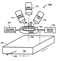
Figure 7 is a perspective view of a substrate treatment
system, according to the present invention, showing three lasers
directing energy (beams) through a nozzle towards a 6urface of
a substrate.
Figur~ 8 is a cross-sectional view of a substrate supported
on a pedestal, for surface treatment according to the present
invention, particularly illustrating a flat plasma that may be
f ormed according to the techniques of the present invention .
Figure 9 is a schematic view of the major, ~lts of
a system, such as the sy6tem of Figure 7, according to the
present invention.
Figur~ 10 is a graph illustrating a sequence of operating
the various ~ ts of the system of Figure 7, according to
an example of the present invention.
Figure~ lOA, lOB, loC ~n~ loD are graph, chart and graph,
respectively, of operating parameters for an excimer, Nd:YAG and
C2 laser, according to an ' ~ t of the present invention.
Figur~ llA is a photomi~:LuyL~ of a surface of a prior art
tungsten carbide substrate prior to surface treatment,
exhibiting grinding marks and surface contamination.
Figuro llB is a photomicrograph of the surface of the
tungsten carbide substrate of Figur~- llA, after the pre-
treatment regime of the surface treatment process of the present
invention .
Figure llC is a photomiuLuyLc-ph of the surface of the
tungsten carbide substrate of Figur~t llB, after the coating
regime of the surf ace treatment process of the present
invention .
F$gure llD is a Raman spectrograph taken of the surface of
the tungsten carbide substrate of Figure llC, which was surface
treated according to the present invention.
Figure llE is a photomicrograph representation of a cross-
section of the tungsten carbide substrate of Figure llC, which
was surf ace treated according to the present invention .
Figure llF is a photomi.:LUyL~ph of a diamond coating
38
.
SUBSTITUTE SHEET (RULE 263
~ w0 95l202s3 ~ 1 i8 1 ~ ~ 0 ~ P~ o~
exhibiting 1,0,0 crystal orientation, fabricated according to
the techniques of the present invention,
Figure 12A is a detail~d view of beam cross-sections and
intersection, according to all example of the present invention.
Figure 12B is a side view of a substrate being surface
treated, according to an example of the present invention.
Figure~ 13A through 131~ are views of tailorable coatings
that can be fabricated on substrates, according to the present
invention .
Figure 13I is a pe~a~e~:Live view of a three-dimensional,
physical object that can be fabricated using the coating
techniques of the present invention, and ~ LL~tes the truly
heteroepitaxial nature of the techniques.
Figures l~A anC l~B are perspective views of long tubular
substrates being treated according to the techniques of the
present invention.
Figur~s 15A an~ 15B are cross-sectional views of ball
bearings that have been coal:ed according to the techniques of
the present invention.
Figure 16A is a side view of a round tool being surface
treated, according to an pmhotl;- ~ of the present invention.
Figur~ 16B is a side view of a round tool being surface
treated, according to another embodiment of the present
invention .
Figur~s 16C an~ 16D are side and end views, respectively,
of a round tool being surf,~ce treated, according to another
t of the present invention.
Figuros 16E is a side view, respectively, of a round tool
being surface treated, according to another Pmho~i- t of the
present invention.
Figur~s 16F is a side view, respectively, of a round tool
being surface treated, according to another Pmho~;- t of the
present invention.
39
SUBSTITUTE SHEET (RULE 26)
wo ss/202s3 ~
.~T~TT T n DES~`RTPTION OF THE INVENTION
As used herein, the term "surface treatment" means altering
the metallurgy of a substF,at~e, including "fabricating" one or
more coating layers t o~n the surface of a substrate or on a
5 surface of a previously fabricated coating, as well as modifying
the composition of the substrate in a sub-surface region
("conversion" or "transition" zone) below the surface of the
substrate. Two surface treatment "regimes" are described -a
"pre-treatment" regime in which the substrate is prepared for
10 subsequent coating by any suitable coating technique, and a
"coating" regime in which a coating is fabricated on the surface
of the substrate. As used herein, the term "substrate"
includes an article such as a flat or round cutting tool, and
is also applicable to a selected area of the article receiving
15 surface treatment. Generally, the coating technique of the
present invention involves extracting and reacting a
"constituent" (or "primary") element from the substrate,
reacting it in a "reaction zone" immediately above the surface
of the substrate, optionally introducing a "~err~nrl~ry element"
20 from a "secon~l~ry source" to augment the reaction, and diffusing
a "composite material" (the reacted material, having its
physical structure, including phase, altered, modified, changed,
and/or that has had another one or more elements added to it)
back into the substrate. In this manner, in the transition zone
25 there will be "artifacts" of the composite material and/or
fabricated coating material evident, and the fabricated coating
will be "diffusion bonded" to the substrate.
Reference will now be made in detail to the pre~erred
F~mho~ s of the invention, examples of which are illustrated
30 in the ~c- -nying drawings. While the invention will be
described in conjunction with the preferred ~ s, it will
be under6tood that the described embodiment6 are not intended
to limit the invention to those ~mho~;r ts. On the contrary,
SUBSTITUTE SHEET ~ULE 26
~ wo s5/20253 2 1 g l 4 ~ Q r~
the invention is intended t~ cover alternatives, modif ications
and equivalents, which are intended to be included within the
spirit and scope of the illVention as def ined by the claims
;'rp~n~d hereto
In the main, hereinafter, examples of fabricating a diamond
coating on a tungsten carbide cutting tool insert are tl;~cllcc~-d.
However, as will be evident, the invention is not limited by
these materials.
SUBSTinJTE SHEET (RULE 26)
W095/20253 Y2`~ r~l,.s c /~,2 0
PROCESS FLOW CHART (Fiqure 1)
Flgure 1 is a diagram showing the overall flow loO of the
technigues that can be implemented, according to the present
invention. Generally, the technigues all involve directing
5 laser energy (preferably from three distinct lasers) at a
surface of a substrate to drive a reaction system based on
constituent elements, and introducing ~conrl~ry elements at
ap~Luyliate ju.,cLuLas into the reaction system. As will be
evident, the process can proceed in various directions, and may
10 be terminated at various points in the process f low.
In a first process step (~tep A), the laser energy is
utilized to:
mobilize one or more constituent elements in a sub-
surface region (zone) of the substrate, at corresponding one or
15 more rates, and moves the one or more constituent elements
towards the surface of the substrate to produce a ~_ùl~cellLL~tion
gradient of the one or more constituent elements in the sub-
surf ace z one;
separate (from other materials within the substrate) and
20 vaporize selected amounts of a sPlected portion of the one or
more constituent elements in a controlled manner; and
react the vaporized one or more constituent elements in
a prPl imin~ry gas reaction (PGR) occurring immediately above the
surface of the substrate to modify the physical structure and
25 properties of the vaporized one or more constituent elements.
The combination of modif ied and unmodif ied constituent
element(s) is a "composite material". This step (E~tep A~
essentially prepares the substrate for further proc~sin~, as
described with respect to 13t~p B. The process may also be
30 terminated at this stage, as indicated by ~;t~p H.
In a process atep B, the compo5ite material is diffused
into the surface of the substrate creating a "conversion zone"
42
SUBSTlTUrE SHEET (RULE 26)
~ WO 9!il20253 ~ ~ 81~1~ 0 r~l,u~
extending into the substrate from the surface of the substrate.
This is essentially a process of passive diffusion from a
greater ~:u..ce..LLtltion of composite material in the PGR to a
lesser concentration of com]posite material in the substrate.
5 The process next proceeds in one of two directions (8tep~ C ~nd
D, described hereinbelow).
In a process 8t~p C, the process can be stopped, at the
point of having successfully formed a conversion zone exhibiting
a controlled cu~ l L- ~ion of composite material. For example,
10 the composite material in the conversion zone may be diamond or
DLC. As a general proposition, the production of a composite
material, and its diffusion into the conversion zone, does not
alter the volume of the substrate.
Alternatively, (i.e., to 8tep C), in a process 8tep D, the
15 conversion zone can further be treated by rèpeating the steps
of mobilizing, vaporizing and reacting (in a manner similar to
St~p A) the composite material within the conversion zone, or
mobilizing, vaporizing and reacting the one or more of the
constituent elements from the substrate, or both. In the case
20 of further treating the composite material wi~hin the conversion
zone, the process acquires synergy and will proceed at a greatly
increased rate (e.g. exponentially). This process is iterated
to achieve any desired .:o~c~l.LLtltion of composite material at
the surface of the substrate, and any desired gradient of
25 composite material within the conversion zone.
At this point in the process, a coating can be fabricated
on the surface of the substrate. The coating, or fabricated
material, can have an entirely different chemistry than that of
the conversion zone. To fabricate the coating, a s~conrl Iry
30 source may (8tep E) or may not (8tep F) be introduced to the
system .
43
SUB~S`TITUTE SHEET (RULE 26~
W0 9sl202s3
In a process 8t~p E, a ~c~rnn~lAry~ source (the substrate
itself is considered the "primary" source) is activated to
introduce one or more "q-~c~-nrlAry" elements (the one or more
constituent elements of the substrate are considered to be
5 "primary" elements) to the reaction system. The energy source
is used, in this case, to fabricate a synthesized coating
composition (such as diamond or ~;; like carbon) on the
surface of the substrate. The synthesized coating composition
is a fabricated material containing both the one or more
10 seCon~l~ry elements and the composite material, which may be the
~;ame as one another or dif f erent than one another .
As noted above- (e.g., 8t~p D), a conversion zone will be
rormed below the surface of the substrate. This conversion zone
may comprise a primary conversion zone and a secondary
15 conversion zone between the primary conversion zone and the
surface of the substrate. Generally, the sernn~ry conversion
zone will have a relatively small depth, as compared with the
primary conversion zone, and will have a grezter concentration
of the one or more sernn<l~ry elements than are present in the
20 primary conversion zone. The secnn~Ary conversion zone, in
conjunction with the primary conversion zone, provides an
important function vis-a-vis bonding, support and stress
distribution for subsequent fabrication of a coating on the
substrate . The conversion zone (primary and 5er. n nrl;~ry) has an
25 overall inf luence in def ining the parameters required for
bonding, support and stress distribution f or a subsequent
coating, if any, f abricated on the substrate . In this manner,
a conversion zone having a depth ~ can be f ormed below the
surface of the substrate, and a coating material of ~hir~nF-cs
30 "t" can be fabricated on the surface of the substrate.
For example, to fabricate an approximately 3 mm
(mi 111- ter) thick layer (coating) of diamond on a steel or
cemented carbide substrate, the primary conversion zone could
44
SUBSTITUTE SHEET (RULE 26
2~ 4~0
0 Wo 95l20253 P~ll u.. j ~ /D~
be approximately 0.75 mm deep, and the secondary conversion zone
could be approximately 0 . 25 mm thick.
Alternatively ( i . e ., to the 8tep E), in a process 8tep F ,
wherein a sec~d~ry source is not il~Loduc;t:d to the sy6tem, a
small amount of the composite material from the conversion zone
is mobilized, vaporized and reacted (in a manner similar to the
8t~p A) to form a 5~nnd~ry c3nversion zone below the substrate,
which can further be reacted (by the energy source) to form a
coating on the substrate. This results in a coating being
fabricated on the substrate which is likely to be thinner than
the coating that was fabricated using a s~cnnd~ry source (8tep
E). It is, however, entirely possible that there will be a
sufficient amount of constituent element available in the
substrate itself to fabricate a relatively thick coating on the
surface of the substrate in the 8t~p F.
For example, using a substrate of tungsten-carbide (e.g.,
92%) in a cobalt matrix, the energy source will cause the
tungsten and the carbide t~ dic~ccQ~ te into tungsten and
carbon form, and the carbon will be the constituent element
("native" source) for fabricating a diamond or DLC coating on
the substrate. Additionall~, dissolved carbon in the cobalt
matrix also provides a "native" source of carbon f or the
fabrication of diamond or DL~- coating.
The surface LL~a~ L technique of the present invention
is superior to prior art CVD (and PVD) processes in that in
those processes cobalt will exhibit an undesirable graphite-
forming influence in the system which will "poison" the system
and inhibit the formation of a diamond coating or DLC coating.
Using the technique of the present invention, any graphite
formed in the process will advantageously and continuously be
converted to diamond in the diamond coating being fabricated.
SUBSTITUTE SHEET (RULE 26)
W0 95/20253 r~ m. ,~
Q
Preferably, all of the available graphite is consumed by the
proce6s. However, it is not destructive of the process if a
small amount of graphite remains unconverted into diamond.
In a process 8t~p G (which follows 8tep E in the process
5 flow), as a coating is fabricated on the substrate, a different
(th~n the previously used) secon~l~ry source having different one
or more secondary elements can be introduced to the reaction
system. This will result in a multi-layer coating being
f abricated on the substrate .
For example, starting with a tungsten carbide substrate,
an overlying coating ( layer) of titanium carbide can be
fabricated, over which a layer of titanium nitride can be
f abricated, over which a layer of diamond can be f abricated, by
sequencing the introduction of s~ n~ry elements into the
15 reaction system.
By way of further example, a thick diamond coating could
be overcoated with a thin coating of cubic Boron Nitride (CBN).
The process is also suitable for fabricating a coating of
diamond on silicon nitride.
The process can also be employed to fabricate a composite
~LLU~;LULe of diamond and CBN, or vice-versa, or to f2bricate a
composite structure of diamond particles mixed with silicon
c~rbide or silicon nitride.
As represented by a process 8t~p 1~, it may be desirable in
some instances to avoid (or minimize) dif~using the composite
material back into the substrate (see 8tcp B), in which case the
process can be stopped after mobilizing, vaporizing and reacting
the one or more constituent elements of the substrate in the
8tep A. This is advantageous for fabricating a very thin
46
SUESTITUTE SHEET (RULE 26)
~ W0 95l202s3 218 ~ c~
coating on the surf ace of t~le sub6trate .
For example, it may be desired to form a thin coating of
diamond or DLC on the surface of a substrate (e.g., a copper
wire), or below the surface of the substrate, without affecting
5 the original volume (e.g., climensions) of the substrate. For
example, material compositions of selected areas or the entire
area of ball or roller bearing tracks or races may be onh~nl-Pd
without affecting their vol~me.
It is also possible that the process flow can proceed
10 directly from the initial mobilizing, vaporizing and reacting
(8t~p A) to the step (8tep E) of introducing a secondary source
to the reaction system. (This "bypass route" is considered a
process step, and is shown as process ~tep I in the diagram of
Figure 1 ) .
For example, in order to fabricate diamond on a pure
titanium 6ubstrate, it woul~l be nPc~cs~ry to introduce carbon
as a secondary element to l:he system (there being no carbon
available as a constituent element in the substrate). ~he step
of mobilizing, vaporizing and reacting the titanium from the
20 substrate will serve to form a diffusion bond with the
subsequently fabricated diamond or DLC coating.
For example, starting with a silicon substrate, carbon can
be introduced by the ~ecrln~l~ry source to produce silicon with
silicon carbide in the conversion zone. ~hen, the silicon
25 carbide can be converted to diamond. Or, for example, nitrogen
c~n be introduced by the &e~ n~l~ry source to produce silicon
with silicon nitride in the conversion zone and, if desired, the
seconrl~ry source can be se~uenced to provide carbon in the
reaction sy6tem for forming a diamond or DLC layer over the
30 conversion zone.
47
SUBSTITUTE SHEET (RULE 26)
~1 8~ P~
CONVERSION ZONE(S) (FIGURE 2A)
Figur~ 2A shows a ~:Luss-section of an exemplary treated
substrate 200 that has been treated according to the techniques
of the present invention, according to one or more of the
5 proces6 6teps described with respect to Figure 1. Therein is
6hown a substrate 202 having a top surface 204, a secondary
conversion zone 206 formed below the surface of the substrate,
a primary conversion zone 208 formed underneath the secondary
conversion zone 206, and a coating 210 that has been fabricated
10 on the surfacQ of the 6ubstrate. The treated substrate 200
could result, ~or example, from performing the process 8t~p~ A,
B, D and E (of Figure 1). As noted above, the c~rr~nrl~ry
conversion zone 206 will have a thickness (d2) typically less
than the thi~-kn,,Fc (~1) of the primary conversion zone, and will
15 exhibit a greater concentration of composite material than the
primary conversion zone. In aggregate, the depth (d) of the
conversion zones is dl ~ d2 ~ d. The thickness of the
fabricated coating is "t".
MULTI--LAYER COATINGS (FIGURE 2B)
Figur~ 2B shows a ~:Loss-scction of an exemplary treated
substrate 220 that has been treated according to the techni~ues
of the present invention, according to one or more of the
process steps described with respect to Figur~ 1. Therein is
shown a substrate 222 having a top surface 224, a first coating
layer 226 of thickness "tl'l formed atop the substrate surface
(the primary convercion zones and cl~ n~lAry conversion zones are
omitted from this figure, for illustrative clarity), a second
coating layer 228 of thirkn~Fc "t2" formed atop the previous (as
viewed) surface of the first coating layer 226, and a third
coating layer 230 of thickness "t3" formed on the top (as
viewed) surface of the second coating layer 228. Such a
treated substrate 220 could result, for example, from performing
48
SUBSTITUTE SHEEr (RULE 26)
~ Wo gs/20253 2 ~ 8 ~ ~ ~ O P~
the process 8teps A, B, D, IB ~n~ G (of Figure 1).
According to a feature of the invention, a multi-layer
coating such as is shown ill Figure 2B is readily fabricated.
For example: the first coating layer 226 can be formed from a
5 com~ination of a constitue lt element of the substrate and a
first Srronr7s7ry element introduced into the reaction system by
the s~cnn~7Ary source; the second coating layer 228 can be formed
from a combination of a constituent element of the first coating
layer 226 and a second secondary element introduced into the
10 reaction system by the secondary source; the third coating layer
238 can be formed from a com~bination of a constituent element
of the second coating layer 226 and a third s~cnn-7.;7ry element
introduced into the reaction system by the secondary source.
~"Pnr7;n~ on the applicati~n, any number of layers can be
15 fabricated, having a predet~7-m;nPd material composition.
This r7. - L~c.tes one aspect of the f]~Y;h7 1 ~7ty and
controllability of the reaction system, namely, the nature and
composition of a fabricated coating can easily be det~rn7;nP~7
simply by the inLL.,du~ Lion of, in this case, a sequence of
20 different sP~o 7~7~ry elements into the reaction systcm. As will
become evident in the ~; CCl7CCinn that follows, there are many
additional features of the technique of the present invention
that allow a high degree of controllability and selectivity in
the ~77hs7n( ? 7t of material ~-omposition, including fabrication
25 of coatings.
EN~T~c.Y S07JRÇE(S) (FIGT7T~T~ 3)
Figure 3 illustrates, schematically, the operation of a
surface treatment system 300, according to the present
invention. Three separate and distinct lasers 312, 314 and 316
30 each direct a beam, via a resE7ective beam delivery system (BDS)
322, 324 and 326 onto a surface 304 of a substrate 302. As
49
SUBSTITUTE SHEET (RULE 26~
Wo 95l20253
illu6trated, the beams are directed to c:u~lve:ly~: on a 6elected
area 330 of the substrate, indicating that selected areas (each
less than the entire surf ace) of a surf ace of a substrate can
bQ treated. In order to treat the entire surface of the
5 substrate, either (a) the selected area (330) must be equal to
or greater than the total surface area of the surface of the
substrate, or (b) a - ~-hAn;Fm must be provided for causing
relative motion between the substrate and the beams, to "scan"
the selected treatment area across the entire surf ace of the
10 substrate. In thi6 figure, it i5 illu6trated that the sub6trate
can be moved relative to the beams, in the direction indicated
by the arrow 332, thereby causing the selected area whereat the
beams converge to move in an opposite direction indicated by the
arrow 3 3 4 to surf ace treat an area greater than one selected
15 area of the substrate. One having ordinary skill in the art
to which the invention most nearly pertains will understand that
various robotic/automated/positioning r- ~n;Fm~ can readily be
employed for cau6ing such relatiYe motion between the substrate
and the beams, and that the &rAnn;nr~ path may be controlled in
20 any suitable (desired) manner. For example, the substrate 302
may be held in a positioning ~ niF~, such as in the end
effector (e.g., x,y,z) of a multi-axis robot, in which case it
will be possible to move the substrate in any of the x, y and
z directions, which is useful for treating 6ubstrates of complex
25 ~e ~y and/or multiple surfaces of a 6ubstrate. For a flat
~iub6trate, having a substantially planar surface, it i6
acceptable to move the substrate with a 6impler --~h;~n; cm.., such
a6 with an x-y positioning table. However, it may be nr~rr~c6;~ry
for specific applications desirable to control additional
30 configurations, including controlling the focal points and
angles of the beams. One of ordinary skill in the art to which
the invention most nearly pertains will readily understand that
6uch 6canning of the beams themselves can be effected under
computer control (with suitable galvos, or the like), and
35 ~L~ry~ ~ -' to follow any desired path, dwelling on any portion
SUBSTIlUTE SHEET ~RULE ,~6)
~ wo ssno2s3 21~ P._-~/uv,~
of the area of the surface of the substrate for any desired time
and that the energy level an~ f ocal points can also selectively
be controlled. For certaill applications it may be desirable
to have both a device for scanning the beams, as well as a
multi-axis substrate positioning ~h~n;r~, to achieve the
desired results. One advantage of using a robot-type - ~ch~n; ~m
for imparting motion to the substrate is that the same robotic
~ chAn;~" can be used to picl; (retrieve) substrates for surface
treatment and to place (dsliver) substrates after surface
treatment. One of ordinary skill in the art to which the
invention most nearly pertains will readily understand that such
~ v~ t of the substrate can be effected under computer
control, and PIUYL ~d SO that the beam will follow any desired
path, dwelling on any portioll of the area of the surface of the
substrate for any desired time.
The laser energy sources 312, 314 and 316 can be focussed,
diffused, ~ .veLy~d, diverged, transported, or the like by
interposin~ suitable known optical elements for achieving these
~unctions in the path of the beam and which may be controlled
by a computer numerical control. Such optical elements are
generally shown as beam deli~ery systems (BDS) 322, 324, 326.
Each of the three lasers used in the surface treatment of
the substrate contribute to the overall reaction being caused.
Generally:
a first one 312 of the lasers (LASER 1) is used to
vaporize the constituent element (create a gas phase), and to
break chemical bonds in the vaporized constituent element. The
f irst one of the lasers is preferably an excimer laser
operating, for example, at 192, 248 or 308 nm (nanometers).
Such excimer lasers are useful for vaporizing any of a number
of constituent elements. In most instances, the excimer laser
will take a sole or primary (lead) role in causing the
constituent element to vaporize, and in initiating the
51
SUBSTITUTE SHEET (RULE 26)
W095/20253 ~ ~ T~
pr-~l ;~; nAry gas ~eaction (PGR) above the surface of the
6ubstrate. In some instances, the excimer laser will be
supported in these roles by another one (e.g., 314) of the
lasers .
a second one 314 of the three lasers (LASER 2) is u6ed,
primarily, to drive the diffusion function (e.g., 8t~p B), and
also bAlAnl-~ the thermal gas reaction and the stoichiometric
chemistry of the gas phase reactions. This laser is preferably
a Nd:YAG laser, and normally assumes a supportive role (in a
manner of spFAk; n~) to the lead role of the excimer laser. In
some instances (scenarios), the Nd:YAG laser will also aid in
vaporizing the constituent -nt, especially in the context
of bright (reflective) materials, and in some instances the
Nd:YAG laser will assume the lead role and be supported by the
excimer laser ( i . e ., f or some substrate and desired coating
materials, the roles of the excimer and Nd:YAG lasers may be
interchanged). Generally, by using both an excimer and a
Nd:YAG laser, to initiate vaporization of the constituent
element and to balance the reaction, there is an interaction
between the two lasers that keeps the reaction ~- An; F~
b~lAnred out. It is advantageous, in any instance, to use both
of the lasers to support the reaction. For example, if it is
desired to form a diamond coating, the greater power and pulse
capabilities of an excimer laser will normally take the lead in
initiating the gas phase reaction, and will be supported by the
Nd: YAG laser .
a third one 316 of the three lasers (LASER 3), preferably
a C02 laser, is used to balance the thermal, physical, gas and
chemistry reactions occurring above the surf ace of the
sub6trate. The principal role of the C02 laser is to provide
thermal balance, and to avoid there being a substantial thermal
gradient in the reacted gases. The C02 laser will also provide
a minimum temperature balance for the gas reaction, and will
bias the temperature of the reaction. The C02 laser will also
provide synergy between the reaction occurring at the surface
52
SUBSTITUTE SHEET (RULE 26
.
09sl~02s3 ~ 0 I ~
of the substrate and the gas reaction occurring above the
surface of the substrate. In certain instances (i.e., with
certain sub6trate materials), the CO2 laser could also be
employed to initiate the reaction ( i . e ., take over the primary
5 role of the excimer laser with respect to this function).
Although the lasers are shown in Figure 3 as directing
their respective beams onto the selected area 330 of the
substrate from different angles (an converging on the spot 330),
it is within the scope of the present invention that the beams
10 could be directed co~ y at the reaction zone. Generally,
due to the synergy effected by the three lasers, they should all
be directed at the same spot (330) on the substrate.
SECONn~RY SO~RCE(S) (FIGURF 4~
Figure ~. illustrates a surface treatment system 400
particularly suited to introducing one or more secondary
elements. In this figure, the three lasers (e.g., the three
la6ers 312, 314, 316 of Fig~lre 3) are shown as one (combined)
element 410 delivering their beams through a beam delivery
system (BDS) 412. The beams ,~re directed at a selected area 430
(compare 330) of a surface 404 (compare 304) of a substr2te 402
(compare 302), and relative ~notion between the beam(s) and the
substrate 402 is indicated ~y the arrows 432 and 434 (compare
332 and 334~. In the surface LL~ i t system 400 of Figuro ~,
there is also provided at least one s~ n~l~ry source (SECONDARY
SOURCE 1) 420. There may be a plurality ("N") of secondary
sources, as indicated by the s~c~n~l~ry source ('iECI~N~ ?Y SOURCE
N) 422. The one or more s-~c~ ry sources introduce
corresponding one or more ~ ncl~ry elements into the reaction
system (constituent elements of the substrate are considered to
be primary sources for the reaction), and the ~ecnn~l~ry elements
may be in the form of a gas, a vapor, a powder, or other
suitable form, to augment the reaction occurring in the reaction
53
SUBSTITUTE SHEET (RULE 263
WO 95l202s3 '~ X r~
0 ~
zone immediately above the surface of the substrate. The
secondary element is suitably provided by a nozzle (jet)
adequate to direct a stream of the secondary element at the
reaction zone, so that the secondary element(s) can contribute
5 to the reaction that is being driven by the laser beams. It is
preferred that the secondary element(s) be directed towards the
6ame area (430) of the substrate whereat the laser beams are
directed, but it is also possible to introduce the secondary
source at another selected area on the substrate, or to simply
10 "flood" the substrate (i.e., the entire surface of the
substrate) with the s~cn~ ry element(s). By introducing a
secondary element to the reaction, a coating may be fabricated
on the surface of the substrate, for example, as described with
respect to 8t~p E in the process f low diagram of FigUr~ 1.
The secondary element is introduced into the reaction
system by any of a number of known means, such as by spraying,
dispersing, depositing, ablating, or any other known means, and
may be in the any suitable form such as a liquid, a gas, a
solid, a plasma, a powder, or the like.
For example, a gaseous ~rnnrlAry element may be introduced
into the reaction system using a pressurized nozzle ( jet) that
is designed to deliver the gaseous se~nn~lAry element in an
envelope of another (e.g., inert) gas which will focus (direct)
the delivery of the soc nn~lAry element by helically-controlled
swirling of the gases exiting the nozzle ( jet). In this mannqr,
the secondary element can be directed to the same ~ cted area
of the substrate as the incident energy beam. According to a
feature of the invention, the gaseous secnn~Ary element (SS) and
the enveloping (shielding) gas (SG) can both serve as secnn~lAry
elements in the reaction. The secnn~lAry element may also be
s~lectecl to serve as a "shield" (from the environment, without
necessitating the use of a vacuum) for the process when a
secondary source is not needed (see, e.g., 8teps C, F an~ H in
54
SIJBSTITUTE SHEET (RULE 26)
~ woss~o2s3 21~ p~"~
the process flow, described hereinabove), in which case the
SDl ~n~lAry element (and the enveloping gas) may be a clean or
inert ga6. Der~n~lin~ on the treatment, a shi~l-q;n~ function
may not be necessary.
N07 7T T` DESIGNs (FIG13RT ~ 5 . 5A AND 5B
Figur~ S illustrates an ~mhotli ~ of a nozzle 500 suitable
for introducing a gaseous ~c~n~lAry element (from a secondary
source) to the reaction syst~m. In thi6 ' ];- t, the nozzle
500 is suitable for introducing three distinct gases - a gaseous
s~rr~nAAry element (SS), a ~hi~lrlin~ gas (SG) and a "buffer" gas
(BG) .
The nozzle 500 is annular, having a ring-like body portion
508 and central axial openillg 506. In use, the nozzle 500 is
disposed above a surface of a substrate (SUBSTRATE) undergoing
treatment. As shown, the three laser beams E1, E2 and E3 may
be directed through the central opening of the nozzle, at the
substrate .
In this nozzle ~ 500, a l::hiP~ gas (SG, such
as nitrogen) is introduce~ through a lower (closest to the
surface of the substrate) irllet 530 of the nozzle, circulates
through a annular runner 532 I~L-~U~ U- the body of the nozzle,
and is ejected via outlet ports 534 to the central opening
(inner rlii - ~r) of the nozzle. A secondary source (SS, such
as carbon dioxide) is introdllced through an int~ i Ate inlet
520 of the nozzle, circulates through a annular runner 522
tllL.,ugh~,u~ the body of the nozzle, and is ejected via outlet
ports 524 to the central ol?ening Of the nozzle. Since the
QCor~ ry source is ejected above (as viewed) the shielding gas,
it is in a position to be re~cted by the laser energy (E1, E2,
E3), and to be enveloped (surrounded) by the shielding gas. A
buffer gas (BG), analogous to a sensitizing agent, may be
SUBSTIIUTE SHEET (RULE 26~
W0 95~202s3 ~ r~
introduced in conjunction with, such as above (a6 viewed) the
secondary 60urce. The buf~er gas is selected (if nP~R~ry) to
assist in the transferring energy from the laser beams to the
5~nnnfl~ry source, and may act as a buffer in breaking down the
5 secondary source. As shown the buffer gas is il~L~uduced through
an upper inlet 510 of the nozzle, circulates through a annular
runner 512 throughout the body of the nozzle, and is ejected via
outlet ports 514 to the central opening of the nozzle. Since
the buffer gas is ejected from the nozzle above (as viewed) the
10 sPnnnl~ry source, it is in a position to absorb laser energy
(E1, E2, E3) for subsequent transfer to the sPcnn~ry source
gas. The nozzle 500 is ~ pnsP~l at a distance "h" above the
substrate, which i5 est;~hl iF:hP~l to provide sufficient time
(i.e., propagation rate times distance) for the gas reaction to
15 substantially complete itself between the nozzle and the
substrate .
Figur~s 5A ~nd. 5B illustrate an alternate, preferred (e.g.,
for fabricating a diamond coating on a tungsten carbide
substrate) Pmhotl;-~nt of a nozzle 550 for delivering a sPcnr~l~ry
20 source (SS) gas and a shielding gas (SG) to the treatment
system, and i8 generally similar to the: '~~'; ~ 500 shown in
Figure 5 in that the nozzle is annular and has a central opening
through which the laser beams (shown by the single arrow
labelled "BEAMS", in Figure 5B) can be directed through the
25 gases towards the surface of the substrate (not shown) being
surface treated. In this Pmho~li- 1, tlle nozzle 550 is
constructed as a "sandwich" of two flat, annular nozzle bodies
552 and 554, tlicposPd one (552) atop the other (554). The top
nozzle body 552 has an inlet 561 for receiving the secondary
30 source (SS) gas, an annular runner 562 for circulating the
sec~n~l~ry source gas evenly ( in a f luid dynamic sense)
throughout the top nozzle body, and a plurality of outlet ports
564 ~; ~=pOfi~'d about the inner diameter (ID) of the nozzle body
552. As best viewed in Figure 5A, the ou~let ports are directed
56
SUBSTITUTE SHEET (RULE 26
o Wo9s/20253 ~ 1 81~
,, ~
tangentially, with respect to the axis of the nozzie body, to
impart a swirling motion (e.g., clockwise, as viewed in Figure
5A) to the ejected secc-n~ry source gas. As best viewed in
Figure 5B, the s~crn~l~ry so~rce gas i8 preferable ejected from
5 the nozzle body 552 flat tco]?lanar) with respect to the nozzle.
This allows the secondary ~30urce gas to be as close to the
incident laser beam energy (BEAMS) as possible, so that the
reaction of the sPcon~ ry source gas can r ^nre immediately.
As will be evident from ~i~cllCcion hereinbelow, the nozzle 550
10 is ~;cprsed at a sufficient distance ("h", see, e.g., Figure 7~
above the surface of the sul~strate to permit the sought after
reaction of the s~con~l~ry source to occur. As shown in Pigure
SB, the chi~l~in~ gas (SG) is introduced through an inlet 580
in the lower nozzle body 554, circulates in a runner 582
15 throughout the lower nozzle body 554, and is ejected via a
plurality of outlet ports 584 to the opening in the nozzle body.
The "p~nings in the two nozzle bodies 554 and 552 are
concentric, and preferably oE the same size as one another. As
best viewed in Figure 5B, the outlet ports 584 for the shielding
20 gas are directed downwards tas viewed~, towards the substrate
being treated. The outlet ports 584 should also be directed
tangentially, with respect to the axis of the nozzle body, to
impart a swirling motion (e. g., clockwise, as viewed in Figure
5A) to the ejected ceCon~1~ry source gas. This results in a
25 "whirling vortex" (re~sel~ed by the line 590) of shielding gas
which will envelope and direct the s~c~n~J~ry source towards the
substrate. For 6implicity of machining the nozzle bodies 552
and 554, the runners 562 and 582 are formed as troughs extending
into the lower (as viewed) surfaces of the respective nozzle
30 bodies. The top surface of the lower nozzle body 554 closes off
the trough (runner 562) in the upper nozzle body 552, and a
simple annular plate 592 having a central opening closes off the
trough ( runner 582 ) in the lower nozzle body 554 .
57
S~J~ST~ F SHET (RULE 26~
W0 9s/20zs3 . ~ i ;, PCr/US95~ 782
~3`~pp~E--TRR~l'MRNT (FIGURES 6A 6B)
Generally, substrates will benefit from ~Le~aLcltiOn of the
surface sought to be coated. Grinding marks and contaminants
may be present on the surface, and should be removed. Polishing
5 and chemical etching are known proces6es f or perf orming pre-
treatment. Generally, rh~mic~l etching of a substrate requires
the hAn~ll in~ of hazardous chemicals, and result in toxic waste,
each of which il,~Loduces added complexity to a system for
coating a substrate. ~I~Leuv~, each substrate composition
10 would require its own rh~mic;~ to perform such etching.
According to the present invention, substrates of various types
are prepared for fabrication of a coating using the same
laser(s) that are already in place for fabricating coatings.
According to a feature of the invention, the surface
15 treatment system (e.g., 300) can be used not only for performing
the surface treatme~t on the substrate, but can also be used to
perf orm pre-treatment . Generally, this is a matter of
controlling the process parameters of the lasers, vis-a-vis the
gases .
Figur~ 6A ~ndl 6B illustrate how a substrate can be pre-
treated, in conjunction with the surface treatment process of
the present invention. The pre-treatment process can be
performed prior to (i.e., separately from), or in conjunction
with, the surface treatment process described with respect to
Figuret 1.
According to the present invention, the pre-treatment
technique o~ the present invention can be used as a "precursor"
to characterize the surface of a DUbaLL"te for any subsequent
coating process, including CVD and the like.
58
SUE~STITUTE SHEET (RULE 26
~ wo gs/20~ ~ 1 8 1~ ~ 0 . ~llu .,_ /8,~
Generally, by way of example, as shown in Figure 6A, a
tungsten carbide substrate 602 will exhibit grains 630 of
tungsten carbide which are ~uLLvullded and covered by cobalt
632. As mentioned herei~above, the presence of cobalt is
somewhat problematic in the context of forming a diamond coating
on a ~iubstrate. This is especially troublesome when the cobalt
is present on the surface of the substrate. According to a
feature of the invention, surface chemistry changes can be
induced in 6uch 6ubstrates, if required. For example, the
chemistry of a tungsten carbide 6ub6trate can be altered to
exhibit 6table cobalt nitride.
According to a feature of the pre6ent invention, a
sub6trate i6 pre-treated by u6ing a one of the la6er6 (e.g., the
excimer la6er) to ablate cobalt (as well a6 60me tungsten
carbide) from the 6urface of the substrate, thereby exposing the
tung6ten carbide grain6 634, and performing other 6ignificant
metallurgical function6 de6cribed in greater detail hereinbelow.
IloLe~v~L, the cobalt can also be reacted to form a 6table cobalt
nitride. The cobalt can be ablated and some WC and Co can al60
be reacted to form 6table carbon nitride or cobalt nitride.
Nitrogen can be introduced t:o form cobalt nitride, if de6ired,
during pre-treatment, to change the 6urface chemi6try of the
substrate, to form stable cobalt nitride or carbon nitride to
assist in crystal orientation, to obtain more 1-0-0 plane
~ . In the prior ar~, it is typical to f irst grow CBN
to prepare the 6urface of tlle 6ub6trate for subsequent growth
of 1-0-0 plane diamond.
Figure 6B l- ~re6~1-L6 a tung6ten carbide 6ub6trate (602)
that ha6 been pre-treated and, a6 6hown therein, the
pretreatment proce66 will al60 re6ult in a de6irable rounding
off of the peak6 of the tungsten carbide graiins. In this manner
(i.e., by pre-treating the substrate to be 6urface
treated/coated), various advantages accrue. Cobalt can be
59
SUB~SrlTUrE SHEET (RULE 263
W0 95/20253 ~ S I~
O
minimized or eliminated front the surface, grinding marks and
impurities can be removed from the surface, and the structure
of the exposed tungsten carbide can be controlled and modified.
Generally, by performing such a pre-treatment process, prior to
5 performing the surface treatment (e.g., coating) process, the
subsequent surf ace treatment process can much better be
controlled, by imparting known (e.g., constant, repeatable)
characteristics to the surface of the substrate being treated.
As shown in Figure 6B, a sub-surface region, extending to a
10 depth ~', has been cleared of cobalt. Generally, this is a
~JLt:~;ULl:~UL to the conversion zone described above. Figuru~ llA
~m~ llB, described hereinbelow, are also descriptive of the pre-
treatment process. Additional detail of the process parameters
is set f orth in the examples described hereinbelow .
In addition to exposing and rounding off the tungsten
carbide grains, the pre-treatment process of the present
invention effects metallurgical changes within the surface of
the substrate. For example (again, in the context of a cobalt-
cemented tungsten carbide substrate), diamond having a 1 , 0 , 0
20 crystal orientation can be formed, which will serve as a highly
desirable nucleation site for subsequently fabricated diamond
tor DLC) coating on the surface of the substrate. Again, this
is irrespective of the technique used to coat the substrate, and
is useful for CVD processes and the like. However, as will be
25 evident, using the coating fabrication processes of the present
invention will result in a synergistic effect, and exponential
results, since the same laser equipment is used both to pre-
treat (prepare, characterize) and to treat (fabricate a coating
on) the 6ubstrate. Moreover (again, in the context of a
30 cobalt-cemented tungsten carbide substrate), the pre-treatment
process of the present invention advantageously forms a complex
of carbon + nitride + cobalt-nitride or prescribed orientation
in the valleys between the tungsten carbide peaks which is
highly suitable for subsequent coating (or for simultaneous
SU~llUTE SHEET (RULE 26
wo gsl202s3 2 ~ , r ~ ".
fabrication of a coating).
SURF,ACE TR~Al'M~NT AND pRF--~R~M~NT SyS~RM (FIG~TRF 7)
An overall process flow (Figure 1), the use of three lasers
(Figure 3), introduction of a secondary source (Figures 4, 5,
5 5A, 5B) and pre-treatment (l~igures 6A, 6B) have been described
hereinabove .
Figure 7 illustrates a complete surface L ~ai ~ system
700, suitable for performing the entire repertoire of process
steps outlined in Figure 1, utilizing the three laser process
10 described with respect to Figure 3, including introducing one
or more secondary sources a~ di p.r'lqg~tl with respect to Figure
4, incoL~oLating a preferred nozzle design such as was described
with respect to Figur~s 5A ~,n~ 5B, and suitable for performing
the pretreatm~2nt described ~i~ith respect to Figur~s 6A an~ 6B.
The surface treatment system 700 includes three lasers: an
ultraviolelt excimer laser ~LASER 1) 712, an infrared Nd:YAG
laser (LASER 2) 714 and an infrared C02 laser (LASER 3) 716.
Each laser emits a beam whi( h is directed through the opening
of the nozzle 722 towards the surface of the substrate 702. The
nozzle 722 has an axis 723 which is preferably normal (at 90)
to ~he surface of the substrate 702. The excimer laser 712 is
directed, at a first angle ~el~l~ towards the surface of the
substrate. The Nd:YAG laser 714 is directed, at a second angle
"'~2", towards the surface of the substrate, The C02 laser 716
is directed, at a third angle "e3", towards the surface of the
substrate. In an exemplar~ ;r L of the invention, the
first angle el = o (parallel to the axis of the nozzle), the
second angle e2 = -30, and the third angle e3 = +30. However,
it is within the 6cope of t~lis invention that the three laser
beams can be directed coaxially or in parallel with one another
(el~e2~e3 = oo) through the opening of the nozzle is within the
61
Sl IBSrtME SHEE'r (RULE 26~,
WO95/20253 ~$1~Q` ~ P~
scope of this invention. The nozzle 722 is ~; qpoq~ at a
standoff di6tance "h" above the surface of the substrate 702.
A gaseous secnn~q~ry source (SS~ 720 (e.g., a carbon-
containing gas, such as carbon dioxide) is provided through the
nozzle 722, and a shielding gas (SG) 724 (a non-reactive or
inert gas, such as nitrogen, helium, argon, or the like) is
provided thorough the nozzle. Generally, the three laser beams
are directed through the nozzle to CUI~V~=LY-: on a selected area
of the substr~te 702, in the manner discussed hereinabove with
respect to Figur~ 3. However, it is within the scope of this
invention that the three laser beams are sized so that each beam
completely covers the surface of the substrate (the selected
area ~1 -qq~q the entire surface of the substrate). In this
example, the substrate is a rectangular substrate, having
ll~r ~innq ~X~ and "Y", and is moved (arrow 732) during surface
1 - ~ai L in the y-axis.
In use, with the gases (720, 724) turned on, a plasma (not
shown in this figure, see Figuro B) is formed beneath (as
viewed) the nozzle, immediately atop the surface of the
subqtrate 702. As mentioned above, the E~conr~ry source is
converted in the plasma, along with vaporized constituent
elements, to fabricate a coating on the surface of the
substrate .
Generally, the role of the excimer laser 712 is ~o perform
surface ablation, break down the E~cnnrl Iry source (SS) and
initiate synthesis for bonding and growth (fabrication) of a
coating on the surface of the substrate; the Nd:YAG laser 714
assists the excimer laser in breaking down the secondary gas and
performs a prominent role in diffu5ion; and the C0z laser 716
helps maintain the thermal balance of the reaction, both in the
plasma and on the substrate. With this in mind, although it is
preferred that all three laser beams pass through the nozzle,
62
~JESTITUTE SHEET (RULE 26
W095l20253 ~ 0 P~
it is within the scope of this invention that the beam from the
Coz laser 716 could be directed into the plasma without passing
through the opening in the noz21e.
SUBSTRATE SUPPORrr AND FTA'r pTA~M~ (FIGURE 8)
~ ,, i
Figure 8 illustrates apparatus for supporting a substrate
802 being treated, and a preferred shape of the plasma
t"PLASNA") being generated in the surface ~L~ai nt process.
A distinct advantage of the present invention is the
ability to form a flat plasma that is closely adjacent the
surface of the substrate being treated. Noreover, such a flat
plasma can wrap around the corners of the substrate, and is
advantageous in the fabrication of coatings on round tools such
as drills. Generally, the plasma "delivers" secondary elements
to the surface of the substrate, and ensures localized (versus)
mass heating of the substrate.
In this example, the substrate 802 is disposed atop a
pedestal 804 which has a button-like projection 808 extending
upward from its top (as viewed) surface. The projection 808 is
preferably smaller in area than the substrate being supported,
and the substrate is disposed concentrically atop the
projection. A vacuum passage 810, passing through the pedestal
804 is suitable for ''rhllrklnrJ'' (holding) the substrate onto the
pedestal, and is well suited to automated h~n~l;n~ of substrates
in a production environment.
The plasma shown in FiLgure 8, created by a surface
treatment system such as was described with respect to Figure
7, is a "flat" plasma, in that it is generally coplanar with the
surface of the substrate, ~nd is of controlled, minimal,
vertical (as viewed) extent. By creating a flat plasma,
reactions of vaporized constituent elements (from the substrate)
63
SU~I~ SHEET (RllLE 26~
W0 95/20253 l.~ si ~
4~ 0
and s~ n~ lry elements (from SF~r~n~ry sources) can be well
controlled, and~lbcalized at the surface of the substrate which
is intended to be treated.
The flat (squat) plasma shape, and its intimate contact
with the surface of the substrate, is advantageous in that it
allows for fabrication (growth) of a coating directly on the
surf ace of the substrate . In other words, the f lat plasma
interacts with the surf ace of the substrate . This is in marked
contrast to CVD systems, and plasmas shaped like tall columns,
the coating is "rained" down onto the surface of the substrate.
and allows f or relatively high coating rates of coating
f abrication .
A signif icant advantage of the invention accrues to the
flat plasma that can be formed, and vacuum rhll~k;nq complements
the formation of 6uch a flat plasma. Moreover, as illustrated
in Figur~ 8, the plasma generated by the process of the present
invention can be caused to wrap around the edges of the
substrate being treated. Such wrapping around (the edges of the
substrate) of the plasma can be ~nh~n~ed by providing a
plur~llity of ~ ry vacuum passages 812 through the pedestal,
such that these passages exit the top surface of the pedestal
outside of the projection 808 yet within the area underneath the
substrate. The same (or another) vacuum which serves to hold
the substrate onto the pedestal will serve to augment (enhance)
wrapping of the plasma around the edge of the substrate.
The reaction r- ~n; ! effected by the combination of
lasers and plasma can be classif ied as "pyrolitic" and
"photolytic". Generally, in the pyrolitic r~ ;~n;sm, the
laser ( s) serve ( s ) to:
(a) locally heat the substrate to induce thermal reactions
on the surface where it is desired to fabricate a coating,
(b) alternatively, the laser energy is absorbed by the
64
~;UBS~IME SHEET (RULE 26
o wo 95l 0253 ;~ ~ 81~ ~ ~ PCT/US9SI00782
reactant, which is initially excited into non-dissociative
states. After energy relaxation, the reactant gas can
dissociate to form thin films,
(c) the substrate and the gas can simultaneously be heated,
(d) when the laser directly heats the substrate, gas near
the surface is heated and dissociated by diffusion and
convection -h~n i ~
Generally, in the photolytic - --h~n; Fr1 (or photochemical
process, the laser(s) serve(s) to dissociate gas-phase or
surface-adsorbed molecules to form deposit atoms or
int~ tes- without significantly heating the gas or surface
of the substrate. Laser excitation could occur by stimulating
electronic transitions by the absorption of one ultraviolet
photon or, alternatively, by the absorption of several visible
or ultraviolet photons. In the latter case, absorption may
occur either in a concerted manner, as in multiphoton
absorption, or in a sequential manner which may, in fact,
involve photon absorption by intermediate products. The
photolytic products may further be dFC _ _ 6~ by the pyrolitic
2 0 process .
Generally, the output of an excimer laser can effectively
be absorbed by carbon dioxide (e.g., from the s~cnn~ry source),
which leads photochemical reactions to break down C-0 bonds to
form diamond films or reactive int~ -';;ttes. Since carbon
dioxide is essentially transparent to the output of an Nd:YAG
laser, the Nd:YAG laser output is mainly absorbed by the
reaction int~ te created by the excimer laser, and by the
substrate or by some film overlaying it.
SUSSllME SHEET ~RULE 263
;~ 8 1~ ~ ~ r~ ~ 2 o
~RCT~ING CONTROL OV~R THE SYSTEM (FIGURE 9)
Figuro g illustrates, schematically, an overall surface
treatment 6y6tem 900 (6~ ilar to the 6y6tem 700). A 6ubstrate
902 is ri; ~pOF.-~ underneath a nozzle (omitted from this view, for
illustrative clarity), energy from laser6 910 i6 directed at the
sub6trate to create a reaction within the 6urf ace of the
sub6trate and immediately above the surf ace of the 6ub6trate
(including forming a flat plasma), one or more Ees-n~lAry
element6 are introduced from one or more ~:ec'~n~ Iry sources 920
to augment the reaction occurring at the substrate, the
substrate can be moved around by a multi-axis positioning
ni F~ 930 (e.g., -a multi-axis robot), and the operation of
these components is controlled by a controller 940 (such as a
suitably yloyL ' computer). Importantly, the system can
exerci6e control over the timing (e.g., 6equence of turning on
and off) of the lasers (910), as well as the relationship
between pulses delivered by the various lasers.
R~l~MPLES
There follows examples of pre-treating a tungsten carbide
substrate and fabricating a diamond coating, using a surface
treatment such as is described with respect to Figur~ 7.
In any such process there are, of course, numerous
variables, making the process "recipe" different from one
substrate type (e.g., material, , ~L,y, size) to another.
As aptly noted in the Kabacoff patent (5,176,788), the variables
attendant such a process are vus, complex and interrelated,
making a calculations or prediction6 very difficult. Generally,
a better approach i6 to try different proce66 parameters, within
a reasonable range of parameters, ob6erve the re6ults obtained,
and empirically optimize the process.
66
~uBshTurE SHEET (RI~E 2
wo 9sl202s3 P~~
2181~4~
Generally, a system for fabricating a coating on a
substrate, according to the present invention, comprises three
lasers, each with its own beam delivery system (BDS), employs
a nozzle delivering a second~ry source (SS) in an envelope of
5 a ~ 7~7inr gas (SG), and creates a flat plasma on the surface
of the substrate. More particularly, in the context of
fabricating a diamond coatins on a tunqsten carbide substrate,
the substrate may be pre-treated f or subsequent coating by any
suitable technique for forming a coating on a substrate,
10 ;nrll1~7;n~ the techniques of the present invention, or an entire
surface treatment process may be performed ;~r~ 7;n~ a pre-
treatment regime and a coatinlg regime.
In the examples that follow, a flat carbide cutting tool
insert substrate is pre-treated, or i8 treated (pre-treated and
15 coated) to have a diamond (or DLC) coating. For simplicity, it
i5 assumed that the entire substrate is treated at once ( i . e .,
the beams are of suf f icient dimension to "f lood" the entire
surface area of the substrate). A surface treatment system such
as was described with respect to Figures 7 and 9 is employed.
Figure 10 is a process timing diagram illustrating the
proces6 of pre-treating a substrate for subsequent fabrication
of a coating (or deposition of a coating by a CVD process, or
the like).
Pigure lOA is a process timing diagram illustrating the
process of simultaneously (in-situ) pre-treating a substrate and
fabricating the coating.
Figure llA is a photomi~_LoyLaE,l~ illustrating the surface of
a tungsten carbide cutting tool insert (substrate) prior to such
pre-treatment, and Figure 13.B is a photomicrograph of the
67
SlJB~ltUrE SHEET ~RULE ~
W0 95/202s3 ~ 5 ( /~
0
tungstQn carbide substrate of Figure llA after pre-treatment.
As shown in Figur~ llA the surf ace of the substrate is replete
with grinding marks and impurities. As shown in Figur~ llB the
surf ace of the substrate is cleared of grinding marks and
5 impurities, and tungsten carbide grains are exposed amid valleys
of cobalt (compare Figure 6B).
As shown in Figure 10, the pre-treatment process of the
present invention involves use of the excimer laser only, and
~blated cobalt is suitably removed by the nitrogen shielding
10 gas, which is suitably introduced through the nozzle t550), but
which may be introduced across the surf ace of the substrate by
another, simplistic nozzle (not shown).
Figure loA is a process timing diagram illustrating the
orchestration of the lasers and the secondary and shielding
15 gases in a complete surf ace treatment process including a pre-
treatment and a coating fabrication regime.
Generally, as illustrated by Figure lOA, three lasers (an
excimer laser, an Nd: YAG laser and a C02 laser) and two gases
(C0z as the secondary source, and N2 as the shielding gas) are
20 operated, in concert, to perform surface treatment in two
"regimes" - a pre-treatment regime and a coating regime. Figure
10 is a diagram illustrating the time at which each of these
~- Ls is turned on and turned of f . The numbers on the
timing diagram (e.g., "0", "12", "25", etc.) represent seconds.
As discussed with respect to Figuret~ 6A ~nd 6B, the surface
treatment system of the present invention is suitably employed
to perf orm pre-treatment of the substrate .
Figure 10 illustrates a pre-treatment regime lasting
approximately twenty seconds, in a time interval between "pO"
and "pl", wherein the substrate is pre-treated by the excimer
68
.
~UBSIll UTE SHEET ~RULE 263
ow095l202s3 21~ D p~ r~ ..,.
laser (e.g., 712) only, to prepare the surface of the substrate
f or f urther treatment .
As shown in Figur~ lo, during the pretreatment phase, the
nitrogen (shielding) gas is also turned on to convey ablated
5 material (cobalt, oxides) away from the substrate. Preferably,
the nitrogen is left on for a brief interval (from "pl" to "p2")
after the excimer laser is turned off to ensure that the ablated
material is completely removed from the surface of the
substrate .
The surface treatment technique may be performed, combining
pre-treatment and coating fabrication, as illustrated by Figure
lOA. Therein, at a time "tO" the surface treatment ~
During the entire surface treatment process, extending from
time "tO" to time "t5", the excimer laser (e.g., 712), the
cecnn~s~ry source (e.g., 720) and the cht~ld;n~ gas (e.g., 724j
are turned on.
The excimer laser is operated during the entire surface
treatment process ("tO" thro~lgh "t5"), generally according to
the parameters set forth above. However, the output of the
excimer laser may be modified "on the fly" during the coating
regime, notably to initiate pre-tLeai ~ (in the interval
between "to" and "tl"), and t~ take up "slack" from the Nd:YAG
laser which may be turned off at time "t3" (~ CUCC~d
hereinbelow) . During the surface ~L~a ~ ~ process, the excimer
laser is suitably operated at 450 mJ at a pulse frequency of 280
Hz .
As illustrated by Figur~ lOA, it is not n~c"c~ry to turn
the Nd:YAG laser (e.g., 714) on immediately at "tO". Rather,
its debut into the process (coating regime) can be delayed for
a brief interval of time (e.g., for 5 seconds"). Generally,
during this excimer-only interval ("tO" to "tl"), a leading edge
69
ITUTE SHEET ~RULE 26
wo 95/202S3 ~ r~ ..,s,~
zone of a substrate can be pre-treated (see, e.g., Figure 12B).
Similarly, it is not nrrPcc~ry that the Nd:YAG laser participate
during the entire coating regime, and it may make an early exit
at time "t3", approximately 10 (e.g., 12) seconds prior to
turning of f the excimer laser .
Similarly, as illustrated by Pigure lOA, it is not
n~rPCC;lry to turn on the C0z (e.g., 716) on immediately at "tO".
Rather, it6 debut into the process can be delayed for a brief
interval of time (e.g., for 12 seconds"). Similarly, it is not
n~rPcc;~ry that the CO2 laser participate during the entire
treatment phase, and it may make an early exit at time "t4",
approximately 5 seconds prior to turning of f the excimer laser .
More particularly:
l . First J ARer: The excimer laser plays a principal role
in surface ablation and breaking rh~-mir;ll bonds in the secondary
source (e.g., C02), and has the following beam delivery
parameters:
a. wavelength 192nm, 248 nm or 308 nm (nanometers), in the
ultraviolet range of wavelengths, preferably 248 nm;
b. power output up to 200 W (watts), preferably lOo W (A
lower power, such as 75 W can be employed for round tools);
c. pulse energy up to 500 mJ (millijoules), preferably 450
mJ;
d. pulse sequence frequency (repetition rate) up to 300 Hz
(Hertz), preferably 280 Hz;
e. energy density of up to 30 mJ/mm2, preferably 25 mJ/mm2;
f. pulse length (duration) up to 26 ns (n~nncPrnnllc),
preferably 18 ns;
g. beam profile - rectangular; and
h. divergence - 3 . 5 milliradians (mrad) .
The beam delivery system (BDS) for the excimer laser
SUBSTIME SHEET (RULE 26
W0 95/20253
~ 21~
includes a rectangular lens to deliver a rectangular beam
(focused) having dimensions 1 mm x ~ inch, and the lens is
posPd about 18 inches upstream (towards the laser) from the
nozzle aligned with the nozzle axis.
To perform ~LeL~ e~i -nt only (e.g., Figur~ 6B), the excimer
laser is on for 20 seconds at 350-380 mJ, pulsed at a frequency
of 220-250 Hz, at 100 watts, and performs surface ablation
(removing surface marks and impurities, removing cobalt from a
surface region of the substrate).
To perform a complete surface treatment (i.e., integrating
pre-treatment and coating regimes), the excimer is on for 45
seconds at 450 mJ, pulsed at a frequency of 280 Hz, at 100
watts, and (i) reacts and breaks bonds in the 8e~rnnrl~ry source
(C02), and (ii) initiates syn1 hesis for bonding and growth.
2 . Secon~ T.~ Pr The Nd: YAG laser, which plays a
principal role in the diffusion function suitably has the
following beam delivery paramsters:
a . wavelength 1 . 06 microns (E-6 seconds), in the infrared
range of wavelengths;
b. power output up to 15~0 Watts (W), preferably 1000 W;
c. pulse energy up to 15~ Joules (J), preferably 50 J;
d. pulse spqu~nre frequency, continuous wave (CW), burst
mode, or Q-switch up to 1000 liz (Hertz), preferably 120 Hz;
e. pulse length (duration) up to 20 ms (milliseconds),
25 preferably 1 ms;
f. beam profile - round; and
g. divergence 55 mrad.
The beam delivery system (BDS) for the Nd:YAG laser
includes a circular lens to dsliver a circular beam (diffused)
30 having a radius of ~ inch, and the lens is disposed about 18
inches upstream (towards the laser) from the nozzle at an angle
71
SUBU',TITU~E SHEET lRULE 26)
w095/202s3 ~ b~ Y~ /o~ ~
of approximately -30 (30O in a one direction) from the nozzle
axis .
In a pre-treatment only regime, the Nd:YAG laser is not
operated .
In an integrated surf ace treatment process, including pre-
tre2tment and coating regimes, the Nd:YAG laser is on for at
least a portion (e.g., "tl" to "t3", see Figure loA) of the
process. The Nd:YAG laser is turned on 5 seconds after the
excimer laser is turned on, for 35 seconds, pulsed at a
frequency of 120 Hz, at loOO watts, to (i) assist the excimer
laser in breaking the bonds in the secondary source (C0z), and
to perform a primary (or sole) role in diffusion bonding.
3. Th;rd Laser: The Coz laser, which plays a principal
role in the supporting thermal balance, suitably has the
following beam delivery parameters:
a. wavelength 10.6 microns, in the infrared range of
wavelengths;
b. power output on the order of 500 - 10,000 Watts (W),
preferably 2000 W.
c. pulse sequence frequency up to 25 Hz, pulse up to 25
mi.:L.,s~ uyel-~ulse frequency up to 20 RHz (RiloHertz),
and a ~u~_L-pulse width up to 500 micr~ ecl-n~
d. energy density up to 0.32 J/cm2;
e. beam profile - round;
f. divergence - 1~ mm/m; and
g. in a pulse stream mode, a pulse stream duration of up
to 5 seconds.
The beam delivery system (BDS) for the Co2 laser includes
a circular lens to deliver a circular beam (diffused) having
a radius of 3~ inch, and the lens is disposed about 18 inches
upstream (towards the laser) from the nozzle at an angle of
72
.
SUBSrlTUTE SH~ET (RULE 26)
~ wo 95l20~s3 2 ~ 81~ ~ ~ PCT/US95/00782
approximately +30 (30 in a direction opposite the direction
of the Nd:YAG laser) from the nozzle axis.
In a pre-treatment only regime; the CO2 laser is not
operated .
In the integrated pre-treatment and coating process, the
C02 laser is turned on approximately 12 seconds ("t2"~ after the
excimer laser is turned on, for a duration of 28 seconds, pulsed
at a -.u~:L-~ulse frequency of 1.5 kHz, at 2000 watts, to (i)
maintain thermal balance during the process (synergy between the
surface reaction and the gas reaction) (ii) change of absorption
rate changes during the process (iii) control the substrate
temperature at the order of 1 ns (nanosecond). The C02 laser
may be turned off shortly prior to the end of the process (e.g.,
at time "t4l').
Generally, the pulsations of the excimer and Nd:YAG lasers
work together to "hammer" (create a shock wave, stress, and
relax) the at the cnmrnn~nts of the plasma, dissociating same,
inter alia. To this end, the phase relationship between the
pulses delivered by these two lasers are preferably adjusted
(coordinated) to optimize the concerted hammering, d~r~n~inq
upon the particular application of the system. These parameters
are, at best, empirically det~rmin~
4 . ~Am Del lverY SYstem The beam delivery system (BDS)
conveys the laser beams to a surface ~Laai -I L "cell" (area for
performing surface treatment), est Ihl i~:h~': the cross-section and
focus of the beams, includes the lenses described hereinabove
for each of the three lasers. Suitable, the excimer beam is
delivered as a rectangular (cross-section) beam, and the beams
from the Nd:YAG and C02 lasers are delivered as circular (cross-
section) beams.
~3
SUBS~lTUTE SHEET (RU~E 26
W0 95l202s3 ~ 6 ` r~
5. ~hi~ldin~ Gas: The shielding (inert~ gas (SG), which
isolates the &Pr~nflAry element (SS) from the ambient environment
(e.g., air) is suitably nitrogen (N2), delivered by the nozzle
(e.g., 550) in gaseous form.
During a pre-treatment only regime, the nitrogen gas in
introduced during the pretreatment period (0-20 seconds) at a
flow rate of 40 sccm. The nitrogen gas removes the ablated
cobalt or oxides. At the termination of the pretreatment
regime, the nitrogen gas remains f lowing f or a f ew additional
seconds to ensure that undesired (e.g., ablated) elements are
completely flushed (directed) away from the surface o~ the
substrate .
During an integrated surface treatment process, the
nitrogen gas is introduced during the entire treatment period
(e.g., 45 seconds, while the excimer laser is turned on), at a
flow rate of 25 sccm. During the process, the nitrogen gas
stabilizes and shields (i.e., from the ambient atmosphere) the
process. Generally, the purpose of the shielding gas (e.g.,
nitrogen) is to prevent formation of residual oxides (from
combination with a~ ric oxygen). The nitrogen ~:hiP~fl;n~
gas serves to (1) prevent formation of oxides, (2) direct
ablated cobalt and/or tungsten carbide away from the surface,
and (3) if desired, form nitrides (e.g., carbon nitride or
cobalt nitride) for fabricating preferred diamond crystal
orientation in the ~,0,0 plane (see, e.g., Figure llF).
6. SecondarY Element: The carbon-containing sPronflAry
source gas (SS) is preferably CO2, delivered by the nozzle in
gaseous form. Other carbon-containing gases could be used, but
are generally either toxic (e.g., CO) or flammable (e.g.,
30 methane).
74
.
SUBSTITUTE SHEET (RULE 26)
~ w095/20253 21 ~iA ~
During a pre-treatment only regime, it is not n~ce~ccAry to
introduce the carbon dioxide gas, since a secondary source is
not required.
During a comprehensive surface treatment process, the
5 carbon dioxide gas is introduced during the entire treatment
period (e.g., 45 seconds, while the excimer laser is turned on),
at a f low rate of 60 sccm . During the process, the carbon
dioxide gas is broken down (by the lasers) into carbon elements
serving as E~-ond Iry elements augmenting formation of the
10 coating.
7. Noz2ile: The nozzle is ring-shaped, has a plurality of
passages disposed about its inner diameter, and is located
approximately 6 inches above the surf ace of the substrate . This
standoff distance "h" is selected to allow for rliCcor;~tion and
15 reaction of the &~ n~?~ry element prior to diffusion into the
substrate and/or fabrication of the coating on the surface of
the substrate.
8. Substrate: The substrate is a tungsten carbide,
rectangular, cutting tool insert, measuring % inch by ~ inch.
20 Such a substrate may contain 94% tungsten carbide (WzC) with 6%
cobalt (Co) binders. Cobalt has a tendency to migrate to the
surface, which is not desirable for rabricating a diamond (or
like carbon) coating. The objective is to remove cobalt
from the surface (and subsurface region), and this is done with
25 the excimer laser in the pre-treatment regime, taking advantage
of the fact that cobalt evaporates faster than tungsten carbide.
After pre-treatment, tungsten carbide crystals (grains) are
exposed at the surface of the substrate and, beneath the
surface, the tungsten carbide crystals combine with neighboring
30 Co binders to form a desira}~le W2C-Co element. The tungsten
carbide at the surface and the tungsten-carbide-cobalt element
below the surface provides desirable nucleation sites for
SUBSlITUTE SHEET ~RLILE 26
Wo 95l20253 ~ O
~.q~
subsequent diamond growth (during the coating regime).
The surface treatment process was performed on an "of-the-
6helf" R~nn: tal (Latrobe, PA) "K68" grade cutting tool
insert, having 92% WC, 2% Ta(Nb)C, and 6% Co, a fine grain size,
5a transverse rupture strength of 2000 N/mm2 (Newtons per
millimeter squared), a density of 14 . 9 g/cm3 (grams per
centimeter cubed), and an HRA hardness of 92 . 7 .
The 6urface treatment process is also suitable, for
example, for an "off-the-shelf" RPnn ~al (Latrobe, PA) "K313"
grade cutting tool insert, having 93.5% WC, 0.596 Cr3C2, and 6%
Co, an average grain size of 1 ~m (micron), a transverse rupture
.,LL~ny~l of 3000 N/mm2 (Newtons per mi 11 i Ler squared), a
density of 14 . 9 g/cm3 (grams per centimeter cubed), and an HRA
hardne66 of 93 . o .
Generally, the integrated surface treatment process of this
invention is suitable for any "off-the-shelf" substrate, without
requiring modifying (e.g., grinding, etching, etc. ) the
substrate prior to treatment.
9. Plasma Plume: The plasma plume exhibits an oblique
20shape LuLL~u~lding a cross-section of the substrate, and the
substrate is preferably traversed through the plume to coat the
desired area (e.g., entire "top" surface) of l:he substrate.
Figure lOB is a graph of beam power (P ~W), vertical axis~
versus pulse frequency (f (~z), horizontal axis) for the excimer
25laser, operating at three (of several) different power level6
(100 W; 87 . 5 W; 75W) . As noted above, a power of 100 W is
suitable f or treating f lat cutting tool inserts, and a power of
75 W is suitable for treating round cutting tools.
76
SUBSTITUTE SHEET (~ULE 26)
~W095120253 ~ 4~ r~ 3~
Figure lOC is a tabular listing of program ;data for the
Nd:YAG laser. Each program number ~1-13) has set of
c~,LL~a~onding pulse frequency, burst time, pump pulse energy and
maximum frequency.
Figure lOD is a detailed power (vertical axis) ver6us time
(horizontal axis) profile for the COz laser, corresponding to
the generalized parameters described with respect to Figure lOA.
With reference to these Figures lOB, lOC ~nd lOD:
(a) for surface treating a flat cutting tool insert, the
excimer laser is operated wit~ an output power of 100 W (Watts),
with a pulse duration of 400 ms (mi 11; c--cnnrlc), in conjunction
with the Nd: YAG laser operating according to PROGRAN Nll~BER 4
on the table of Figur~ lOC and the Co2 laser operating according
to the profile of Figure loD;
(b) for surface treatincl a flat tool insert, the excimer
laser may also be operated with an output power of 87 . 5 W
(Watts), with a pulse duration of 350 ms (milliseconds), in
conjunction with the Nd: Y~G laser operating according to
PROGRAM NUMBER 11 on the table of Figure lOC and the CO2 laser
operating according to the profile of Figure loD; and
(c) for surface treating a round tool insert (as tlicC~-lc5~d
below with respect to Figure lCA), the excimer laser is operated
with an output power of 75 W (Watts), with a pulse duration of
300 ms (mil 1; cecnn~lC), in conjunction with the Nd: YAG laser
operating according to program number (Program No. ) 11 on the
table of Figure lOC and the COz laser operating according to the
prof ile of Figur~ lOD .
77
SUBSTITUTE SHEE~ ~RULE 26)
Wo ~s/202s3
4~ 0
PHOTO~ICROGRAPEiS AND RAMAN ANALYSIS
The photomicrographs and Raman analysis of Eigur~s llA,
llB, llC, llD ~nd llE relate to the example of fabricating a
diamond coating on a tungsten carbide substrate, set f orth
above.
Figure llA is a top view photomi~;L OU,L ~ph of the specimen
(Prior Art) prior to 6ur~ace treatment. As shown therein, an
off-the-shelf cutting tool insert will exhibit a pattern of
grinding marks (evident as oblique lines in the figure) and may
al60 have contaminants on the surface (evident as specks in the
figure). As indicated above, it is preferable to perform pre-
treatment to characterize the surface of the substrate prior to
coating, in addition to ablating cobalt and exposing tungsten
carbide grains. Figure llA, although related to Figure 6A,
shows in greater detail some of the ~h;~ on~eS inherent in
surface treating existing substrates.
Figure llB is a top view photomi.LoyLclph of the sreci~ ~
of Figure llA af ter pre-treatment, according to the present
invention. As shown therein, there are a plurality of tungsten
carbide "hills" 1134 (corresponding to 634 in Figure 6B)
YULLUUllded by cobalt valleys 1132 (CULL~ 1; n ~ to 632 in
Figur~ 6B). In this manner, the surface of the substrate is
pre-characterized for subsequent coating, the tungsten carbide
hills serving as defined nucleation sites for subsequent growth
of diamond (or DLC).
Figur~ llC i8 a top view photomicrograph of the specimen
after coating, according to the present invention. As shown
illustrated therein, a plurality of substantially uniform
diamond crystals (the exposed portions of which appear as
pyramid-like ~LUI_I-UL~S in the figure) have been formed on the
6urface of the substrate.
78
lTUTE SHEET (RULE 26
~ WO 95/202~3 ~181 ~ 4 ~3 r~
Figure llD is a Raman x~e- LL ~ ys aph taken of the treated
sp~c;r~~. The vertical axis is absorption, and the horizontal
axis is wave number. As is evident therein, there is a sharp
(narrow) peak at 1332 cm 1. This provides evidence that the
5 coating contains carbon in the Sp2 crystalline phase, as well as
a noticeable amount of diamond-like carbon. As discussed
hereinabove, such analysis is merely indicative, and is not
dispositive of the "quality" of the coating - actual cutting
test6 should be performed to make such a determination.
Figure llE is a side view (cross-sectional) photomicrograph
representation of the specimen after coating, according to the
present invention. As shown therein, a transition zone 1150
extends from the surface of l_he substrate to a depth ''I~'' into
the substrate 1152, and a diamond (or DLC) coating 1154 having
15 a thickness "t" is evident on the surface of the substrate. In
a specimen that was surface treated according to the present
invention, the depth of the transition zone was observed to be
10 ~Lm (microns), and the thickness of the diamond (or DLC)
coating was observed to be 45 ,um. With 45 seconds of coating
20 regime, this confirms a coa~ing growth rate on the order of
l~m/s (micron per second).
A "telltale" sign that th~ surface treatment process of the
present invention was performed on a substrate are the sporadic
traces (artifacts) 1156 of complex carbides (e.g., with respect
25 to treating a tungsten-carbide cutting tool insert), carbon
nitrides, and the like, readily evident in the transition
(diffusion) zone 1150 of the s~lbstrate. This zone 1150 can also
be termed a "differential compositional layer". These "roots"
(of the coating), or an analogous feature (~lPp~n~l;n~ on the
30 coating material being fabricated and the material of the
underlying substrate) would be evident in virtually any product
(substrate) treated by the surface treatment process of the
79
SUBSt1TUTE SHEET ~RU E 26~
Wo 951202s3
present invention and would serve as an artifact to distinguish
(evidence) products made by the process of the present invention
from products made by other (e.g., CVD) processes, especially
if the substrate is a tungsten carbide substrate having a
5 diamond or ~ d-like carbon coating.
Among the many advantages of the present invention is that
no "seeding" is required to fabricate a diamond coating on a
substrate. Due to the nature of 10CA1; 2ecl heating, overall
(mass) substrate temperatures can be maintained as low as 30C.
SCANNING ACROSS A SUBSTRATE
As mentioned above, the surf ace treatment system of the
present invention is suited to treating selected areas (rather
than the entire surface, at once) of a substr~te. In general,
this is a function of the profile (cross-section) of the laser
15 be~mæ. By suitable sizing and shaping of the beams, the
selected area can span an entire "zone" across the surface of
the substrate, and the substrate can be advanced during
LL~al --~t so that the entire surface of the substrate is
treated .
As noted hereinabove, the beams from the three lasers may
be c~,l.v~ ed on a selected area of a substrate being treated,
and the beams are delivered (generally through a gas nozzle) to
the substrate via respective beam delivery systems (see, e.g.,
elements 322, 324 and 326 of Figure 3). It has been determined,
that the process can be optimized by controlling the prof ile of
the individual beams.
Figure 12A illustrates the beams from three lasers
converging on the surface of a substrate 1202. Generally, the
cross-sections of the beams are selected and controlled with
regard to the dimensions of the substrate being treated. In
~UBSrlTUrE SHEET ~RULE 2E~
O WO 95120253 2 ~ 8 ~ u~
this example, a rectangular substrate 1202 having dimensions
"X" and "Y" is undergoing ~Leai 1 (nozzle omitted, for
illustrative clarity), and i5 being moved alonig its y-axis , as
indicated by the arrow 1232 ~compare 332, 432).
The excimer laser (e.g., 712) is caused by a rectangular
lens 1252 to have a rectangular ~cross-section, profile) beam
1262 of dimensions "~" and "b'l', wherein the dimension "n" of the
beam is generally aligned with the transverse dimension "X" of
the substrate, and the dimension "b" of the beam i6 generally
aligned with the longitudinal dimension "Y" of the substrate.
Generally, the dimension "z~" is larger than, and subsumes the
dimension "X" to ensure that the beam will completely cover a
rectangular section (from one side edge 1202c to an opposite
side edge 1202d) of the substrate. By causing the substrate to
move, relative to the beam (as indicated by the arrow 780), the
excimer beam will traverse ( in the 'y" direction) the entire
surface of the substrate 1202, from a "leading" edge 1202a of
the substrate 1202 to a trailing edge 1202b of the substrate
1202. A beam having such a ~:Lvss-scction would generally be
cnncid~red to be a focused beam.
The Nd:YAG (e.g., 714) and C02 (e.g., 716) lasers are
caused, by spherical lenses 1254 and 1256, respectively, to have
circular cross-section beams 1264 and 1266, re6pectively,
impinging on the surface of t]he substrate at angles e2 and ~3,
respectively (compare Figur~ 7). The two beams 1264 and 1266
may have similar circular cros~-sections of radius "r" although,
as shown, they are introduced towards the substrate from
opposite sides of the excimer beam 1262. Preferably, the radii
"r" of these two beams 1264 and 1266 are greater than the
largest (transverse dimension "X" or longitudinal dimension "Y")
dimension of the substrate.
81
SUBSTlTllrE SHEET (RULE 26
wo ssno2s3 1~ G /~
21~ 0 `''
In Figure 12A, the beams 1262, 1264, 1266 are illustrated
a6 dashed lines, and the resulting pattern of three beams
~;ullvt:L~ing on the surface of the substrate is shown by the
dashed line 1270. Tllis pattern 1270 of beam ~ollv~Lyt!nce would,
in practice, be on the surface of the substrate, and comprises
three portions: (1) a first, generally semicircular portion
1270a comprising the ~ullvO~ nce of the beams from the Nd:YAG
and C02 lasers; (2) a second, generally semicircular portion
1270b cûmprising the uullv~:Lg~ ce of the beams from the Nd:YAG
and C0z lasers; and ( 3 ) a third, generally rectangular portion
1270b comprising the ~o.,v~Lg~nce of the beams from the excimer,
Nd:YAG and C02 lasers, said third portion 1270c disposed between
the first 1270a and second 1270b portions.
Beam prof iles, such as those discussed with respect to
Figur~ 12A were employed in the experiment described above with
respect to coating a tungsten carbide cutting tool insert.
Figur~ 12B illustrates the substrate 1202 (in cross-
section) moving (arrow 1210) under the pattern of beam
CUIlVt!Ly~lCe 1270 (shown in perspective). As the substrate is
advanced (moved) under the beams, the substrate is progressively
surface treated, frûm its leading edge 1202a to its trailing
edge 1202b, as illustrated by a coating 1204 and a cûnversion
zone 1206 in a selected area extending from (and partially over)
the leading edge 1202a of the substrate 1202 towards the
trailing edge 1202b of the substrate 1202. Such a process was
s~ cc~c~fully employed to fabricate a diamond coating on a
tungsten carbide substrate, according to the process parameters
set f orth hereinabove .
TATT --RT n COATINGS (FIGURES 13A - 13~1) ;
The technique of the present invention is useful for
fabricating a variety of coatings on a variety of substrates.
82
SUBSTITUTE SHEET (RULE 26
~ w09s/202s3 2181~ ,I/U~
For example, as discussed with respect to Figure 2B, multi-
layer coatings can be fabricated on the surface of a substrate.
In the figures that follow, .,LI~ exemplary applications of
the technology and products produced by the technology are
5 described. As rliccllc-ed abo~e, selected areas of a substrate
can selectively be surface treated. According to an aspect of
the invention, the sur~ace treatment technique of the present
invention is suitable for fabricating "tailored" coatings on a
substrate .
Figure 13A illustrates a substrate 1302 having four
surfaces 1304, 1306, 1308 and 1310 which can be distinctively
treated according to the teclmiques of the present invention.
A coating 1314 is fabricated on the surface 1304, a coating 1316
is fabricated on the surface 1306, a coating having two segments
(1318a and 1318b) is fabric~lted on the surface 1308, and a
coating 1320 is fabricated on the surface 1310. Assuming that
the beam (not shown) is always incident from the top (as
viewed), the substrate will need to be moved (e.g., scanned in
the x-y plane) in order for the beam to treat a substantial area
of the surface 1304. As shown, the coating 1314 covers less
than the entire area of the surface 1304, and more area than one
reaction zone. It is also evident that the substrate will need
to be rotated in order to treat the side surfaces 1306 and 1310
which are parallel to the beam 1312, and the opposite surface
1308 which is entirely blocked from the beam. 8y rotating
these surfaces into position, they may be treated with the same
ease as treating the surfac~ 1304. As illustrated in the
figure, each of the coatin~s (and segments) may be of a
different thickness and extent (area coverage) than the other
of the coatings. Each coating (and segment) may also be of
different composition than the other coatings, d~p~n~lin~ on the
selection of s~cr~n~lAry element introduced to the reaction system
during the formation of the coating. Primary conversion zones
and s~c~n~ry conversion zones (not shown, for illustrative
83
SUEISTITUTE SHEET (RULE 26)
Wo 9s~0253 2 ~ g 1 ~ ~ . 18~ ~
clarity) below the surface of the substrate may also differ from
surface-to-surface, tl~r-~n~in~ on the process parameters invoked
during the treatment of the particular surface of the substrate.
Figure;13~3 illustrates a feature of the invention wherein
5 different thickness regions of a coating and/or different
coating layers each having a different area coverage can be
fabricated on the surface of a substrate 1322. (Primary and
sc~on~q lry conversion zones are omitted from this figure, for
illustrative clarity. ) In this example, a first coating 1324
is fabric~ted on a surface 1326. A second coating 1330 is
fabricated over a top surface 1328 of the first coating 1324,
and is of lesser extent (area coverage) than the first coating
1324. The coatings 1324 and 1330 can be of similar or
dissimilar composition, and o~ similar or dissimilar thickness.
According to a feature of the invention, the energy (e.g.,
from three lasers) driving the reaction system may be directed
at selected areas of the substrate, and can be scanned in any
pattern on the surface of the substrate, to fabricate any
desired "profile" (e.g., compositions, thickness, shape) or
pattern of coatings on the substrate.
Figur~ 13C shows a substrate 1350 having a "tailored"
coating fabricated on its surface. (Primary conversion zones
and seco-n~ ry conversion zones are omitted, for illustrative
clarity. ) Portions 1338 of the coating are flat. Other
portions 1340, 1342, 1344 are of limited extent (area coverage),
and are fabricated to be thicker than the portions 1338 so that
they extend above (higher than) the portions 1338. Further, the
portions 1340, 1342, 1344 can be formed to be tapered (1340),
to have a flat top surface (1340, 1344), to have steep sidewalls
(1340, 1344), to be rounded (1342, 1344), to have a convex top
surface (1342? or to have a concave top surface (744). Each
portion of the coating illustrated in Figure 13C may be caused
84
SUBSr~TUTE S~IEET (RULE 26
o wo 95t202s3 2 ~
to be of different composition (e.g., by using different
6econ~Ary sources for each portion of the coating).
This illustrates only a few of the complex coating shapes
that can be fabricated using the tP~-hn;q~=Ac of the present
5 invention. For example, chip--breaker Aje~ LLY can be fabricated
on a f lat cutting tool insert as an integral part of the
coating. As a corollary to this, the coating technique of the
present invention is applicable to fabricating coatings having
uniform thickness on substrate surfaces having irregular
10 topology (such as would be the case (e.g. ) with a cutting tool
insert substrate having chip-lbreaker features incorporated into
the substrate itself ~ .
Figur~ 13D illustrates an additional "menagerie" of shapes
that can be fabricated as coating structures on the surface of
a substrate, including cylinders 1352, tubular structures 1354,
conical structures 1356, "L''-shaped structures 1358, curved
structures 1360, and tower-type structures 1362. The tower-
type structure 1362 is t~ ative of a particularly
remarkable feature of the present invention, namely its true
20 heteroepita~ial (omnidirpct;onAl ) capabilities. In order to
form such a coating structure, the base portion 1362a of the
structure is first fabricated to extend away from the surface
of the substrate, then the substrate ( or the energy
source/secondary source) is re-oriented, and growth of the
25 structure is continued in another (orthogonal, as shown)
direction to form the segment 1362b. Another rA--rkAhle feature
of the present invention is that all of the structures shown in
this f igure can be f abricate~ on the same surf ace of the same
substrate, and each structure can have a composition differing
30 from the other structures. By way of analogy, the substrate
can be viewed as a countertop, upon which any number of useful
objects can be placed. (Of course, these objects will be
diffusion bonded to the countertop using the techniques of the
SUBSrllUrE SHEET ~RULE 26)
W095/20253 ~Bl44Q P~ O
present invention. ) For example, a flat planar cutting tool
insert could be coated to not only have a diamond coating, but
BO that the diamond coating is tailored to have its own chip-
breaking geometry (structure).
Figur~ 13E illustrates another remarkable, and useful,
feature of the presènt invention. In this case, a snake-like
coating 1366 is formed on a surface of a substrate 1368 tcompare
1360, Figure 13D). In this case, it is desired to form
different coating compositions in different segments of the
snake. For example, a first segment 1366a can be fabricated to
have a first composition, a second segment 1366b can be
fabricated to have a-6econd composition, a third segment 1366c
can be fabricated to have a third composition, and a fourth
segment 1366d can be fabricated to have a fourth composition.
The r~ ;n;n~ segments can be fabricated to repeat the se~[uence
(first, second, third, fourth compositions) . Alternatively, the
segments can r~:~Lesel,t a code, analogous to storing information
(binary, trinary, quadrary, etc) in the snake. These techniques
are, for example, analogous to forming a diamond (e.g. )
~ ~ . The resolution (size) of the segments is limited
only by the wavelength of the lasers employed to form the
segments, and segments having lateral dimensions on the order
of 308 nm are readily formed. A "snake" of titanium-carbide,
vanadium, and chromium-nitride could readily be formed. The
individual segment can be alternatively magnetic and non-
magnetic, semi-conductive and non ~_ulldu~ l_ive.
Figure 13P illustrates how a number (nine shown) of coating
segments (1372a .. 1372i) can be formed in an array on a surface
of a substrate 1370. Each of the segments of the array can be
30 formed of a different composition, and each of the segments can
be formed of a different thickness. The segment 1372b is shown
having a greater thickness than the r~ ;n;ng segments (772a,
1372c .. 1372i). Any, or all, or the segments can also be
86
SUBSTITUTE SHEET tRULE 26)
Wo 9s~20253 21 C~ O r~ J s ~
Pabricated as a multi-layer structure (compare Figure 2s).
Figure~ 13A-lOF illustral_e the capability of the techniques
of the present invention for fabricating "designer" coatings and
compositions, by utilizing the techniques of the present
5 invention.
Figur~s 13G ~na 13H illustrate te~-hniq~ for treating
cylindrical objects, as exemplary of the ability of the present
invention to coat surf aces that are not f lat . Coating can
punches would be a useful application of such techniques.
In Figure 13G, a cylindrical coating 1380 is fabricated on
a cylindrical substrate 1382. The cylindrical substrate may
be of any length. This illustrates the continuous nature of the
technique of the present invention. For example, the
cylindrical substrate may be a wire (e.g., copper) of
15 extraordinary length (thousands of feet). By passing the wire
through a workstation, the coating reaction can be performed
continuously along the length of the wire.
In Figur~ 13H, it is illustrated how bands 1384a and 1384b
of coatings can be applied at different longitudinal positions
20 along a cylindrical substrate, such as a wire. These bands, of
course, could be s~ -rts and may be magnetic or r gnPtiC or
other properties to different:iate one segment from the other
(compare the snake 1366 of Figure 13E).
RAPID ~KU'l'O'l'Yl~ I N~ (FIGTTT~T;~ 13I)
Pigure 13I illustrates, generally, the truly
heteroepitaxial nature of the invention. The fabrication of
coatings is ~ on one or more (one shown) selected areas
of the surface of a substrate 1390. As will be evident, the
substrate may be a "sacrificial" substrate, which can be excised
87
SUBST~TUTE SHEET (RULE 26~
Wo 95120253 2 ~
from the resulting built up (fabricated~ coating structure(6).
An exemplary coating structure 1392 is shown as being
fabricated (built-up) from a selected area of the surface of the
substrate 1390. This can be considered to be growth in a z-
axis (normal to the surface of the substrate).
By way of example, a portion 1392a of the coating surface
1392 is built-up in the Z-axis to a level "tl", above the
surface of the substrate, at which point the substrate (or
treatment source(s) can be re-oriented (e.g., with respect to
the energy source and the secondary source) so that another
portion 1392b of the coating structure 1392 can further be grown
(fabricated) in a different direction (e.g., parallel to and
spaced apart from the substrate, as shown). The growth of the
portion 1392b can be considered to be an X-axis direction. The
fabrication of this portion 1392b of the structure proceeds to
any desired extent.
Likewise, it i8 possible to re-orient the substrate (or
treatment source(s) ) 80 that growth of the structure 1392
proceeds in a different direction from any point along the
portion 1392b. This is illustrated by a portion 1392c of the
structure being fabricated in what can be considered to be
growth in a Y-axis.
Evidently, the shape (outline and area) of the fabricated
structure 1392 is different between the surface of the substrate
and a level t2 than it is between the levels t2 and tl.
This d ~ ~Lcltes~ in a very generalized manner, the truly
heteroepitaxial (omni-directional) nature of the invention,
namely that coatings (and coating structures, and portions
thereof) can be performed in any direction (e.g., in any of the
X, Y and Z axis). The figure is intended to rl l.L~te that
88
SUBS~ITUrE SHEET (RULE 26)
~wossno2s3 218~Q
a coating structure having a distinct outline at any given level
(e.g., above the surface of the substrate) can be fabricated.
The outline at any of these ~iven levels is not constrained by
the outline of the previous level. Further, the area coverage
5 of the structure at any givell level is not constrained by the
area coverage (e.g., "footprillt") of the previous level. At any
given level (height) above the surface of the substrate, any
outline or area coating structure can be fabricated, and control
over the fabrication is suitably effected simply by taking
10 appropriate cross-sections from a computer-generated
representation of the object sought to be fabricated as a growth
structure, for example. In this manner, a three-dimensional
LU~ LUL~= of ul~- v~ ined shape or form can be fabricated on
a substrate. After fabricatin~g the three-dimensional structure,
15 the substrate may be cut off and discarded, or dissolved away,
or removed by any means i n~ i n~ - -n i c~ 1 or chemical means .
The process of the present invention may be combined with
an apparatus controlled by a Computer Numerical Control (CNC)
system which accepts stereolithographic software files (e.g.
20 .StL) to facilitate fabrication of objects having complex parts.
These objects may be formed from simple, flat, or cylindrical
substrates which are manipulated in a fashion to fabricate
(e.g., prototype) products using the methods set forth in this
invention .
Thus, the apparatus and method according to the present
invention can be used to produce complex prototype parts of
composite materials to finished workpiece dimensions from CAD
data. Furthermore, metal, ceramic, and composite parts can be
produced to a final state, requiring no post-process finichin~
and exhibiting ~nh~n~d physical properties by virtue of
advanced material compositions not capable of being produced by
prior art methods.
89
S~IBSTITUTE SI~EEI (RULE 263
wossno253 ~ b~, X ~ ' r~ c~
TU~BITT ~R STTBSTRATES (FIGTJRES 14A and 14B)
The techniques of the present invention are useful for
coating the inner diameters (ID) of tubular substrates, and are
~CreciAlly useful for coating the ID of tubes having a large
rAtio of length (L) to diameter (D) (greater than 3 :1) .
Yiguro 14A illustrates one technique for coating the inside
diameter (ID) of a tubular substrate 1402. An energy beam 1404
(e.g., from three lasers) is directed into one (open) end 1406
of the tubular substrate 1402. The other end 1408 of the
tubular substrate is closed off, preferably by concave (or may
be convex, not shown~ parabolic reflecting surface 1410 (shown
spaced apart from the end 1408, for illustrative clarity). In
this manner, the beam 1404 will bounce around inside of the
tubular substrate, and treat the entire ID of the tubular
substrate. A sec~n~ ry element may or may not be introduced
into the system, as desired.
Figur~ 14B illustrates another technique f or coating the
ID of a tubular substrate 1412. An energy beam 1414 (compare
304, Figure 3) is directed into one (open) end 1416 of the
tubular substrate 1402. The other end 1418 of the tubular
substrate may also be left open. A secondary element may also
be i-.L-~duced, as indicated by the stream 1420 (e.g., of gaseous
E~conrl~ry element).
For tubular substrates having exceptional depth (e.g., high
L:D), it is possible to dispose a simple (e.g., flat) reflecting
mirror within the ID of the tubular substrate to direct the
incident energy beam to selected areas on the ID of the tubular
substrate. In this manner, selected areas (axial,
circumferential, helical) of the ID can be treated by the beam.
Further, by sequencing the introduction of a secondary source,
the treatment can be varied from c~l.octecl area to selected area,
.
SUBSn~E SHEET (f~.E ~
OW0951~0253 2 1 ~ 1 ~4 ~
in a manner similar to th2t of Figurus 1315, 13F ~m~ 13~).
The present invention is useful for coating any of a number
of substrates, several of which have been ~l;c-l~cc~cl hereinabove.
For example, the inner or outer diameters of a helical
5 tr2velling wave tube could be treated and/or coated, as well as
to produce windows for traveling wave tubes. Resistive heating
elements could be treated and/or coated, for example, to aid in
heat distribution, as well a~ the inner and/or outer surfaces
of cookware. Coatings can be fabricated on replA~ ~ hip
lO joints, and the like, so that a portion of the object being
coated is provided with a low-friction coating (with, if
required, PnhAnc_d high load-carrying capacity), while another
portion of the object is provided with a porous or textured
coating (e.g., to promote bonding ~o a bone surface). Gun
15 barrels, cylinder liners, and the like, can advantageously be
treated by the techniques of the present invention. Razors,
knives and sA~lrol~: can easily have their cutting edges treated
by the technigues of the present invention. Cutting tools, such
as drill bits, can be improved by fabricating stepped flutes,
20 by fabricating a diamond coating on the flank of the tool, and
by fabricating chip-breaker J LLY into the tool, which would
otherwise be difficult to achieve using grinding apparatus.
Diamond, for example, is solu~le with iron, in which case it may
be desired to form a silicon nitride coating on the tool (or
25 other substrate). The present invention is capable of
extracting and forming a composite material with virtually any
constituent (primary) element from a substrate and sPc~Anr~;~ry
element, including silicon, copper, oxygen, nitrogen, boron, and
the like. The application of the techni~iues of the present
30 invention to dry machining are virtually unlimited.
COATING W~AR SURFACES (FIGT~ A 15A and 15B~
Figur~ 15A shows a c A~t 1552 of a ball bearing, which
91
SUBSTlTUrE SHEET (~ULE 26~
w0 95/20253 ~ /8.C
has had the surface of its race treated to have a hard (e.g.,
diamond or DLC) coating 1554. This, for example, will allow for
the bearing to function without (or with less) lubrication, in
much the same manner~as treating machine tools according to the
5 pre6ent invention facilitates dry ~hinin~.
Figure 15B shows a ~ - t 1562 of a ball bearing, which
has had the entire surface of the -nt 1562 treated to have
hard (e.g., diamond or DLC) coating 1566. In this manner, the
coating 1566 will function as a heat sink, 80 as to remove heat
10 from the ball and race, and for protecting against corrosion.
COATING P~oUND TOOLS (FIGURES 16A - 16D)
Figur~ 16A illustrates one ~ nt 1600 of coating a
round tool (e.g., an end mill, a drill, or the like). An end
mill 1602, having a shaft portion 1604, a f luted portion 1606
15 and ~ tip 1608 is aligned, as shown, with its tip facing upward
towards lasers and a nozzle (not shown). In the manner
described hereinabove, a plasma 1610 is generated in the
vicinity of the tip. The plasma 1610 will "wind" its way down
the flutes of the end mill, resulting in a coating being
20 fabricated along the entire length of the fluted portion 1606.
Generally, as will be evident, this ~mho~ir ~ is preferred for
forming a thin film diamond (or DLC) coating along the length
of the fluted portion. In this ~mho~lir 1, a vacuum chuck,
similar to the vacuum chuck (804) previously described, can be
25 used to support the end mill and to assist the plasma winding
down the fluted portion.
Figure 16s shows an alternate: ~ ir ~ 1620 of a
technique for fabricating a coating on a round tool. In this
case, an exemplary end mill 1622 (similar to the end mill 1602)
30 is disposed on its side, with the nozzle and lasers coming from
above (not shown). A pla6ma 1630 is formed at the tip of the
92
SUBSrmJTE SHEET (RULE 26~
~Wo ss/2o2s3 ~ ~ 8 1 ~ 4 0 ~ -
end mill, and is walked along the length of the fluted portion
in a manner similar to what has been described above (with
respect to causing relative motion of a selected area on a
larger substrate). In this c~-nhorli L, the end mill should be
S rotated in concert with wal3cing the plasma along the f luted
portion, to ensure uniform ~ c~lg~ (coating fabrication) along
the length of the f luted portion .
Figur~s 16C ~n~ 16D are side and end views, respectively,
of an end mill 1642 (similar to 1602 or 1622~ being further
10 treated subsequent to deposilting a thin film along the length
of the fluted portion (in th~s manner of Figures 16A or 16B).
In this case, it is desired t,~ form a thick film coating in the
flutes, adjacent the cutting edges so that the thick film aids
in cutting, and the thin film aids in chip removal and reduction
15 of cutting forces. La6ers and one or more ~:pconr~ry sources,
both represented by the arro~ 1644, are directed at a selected
area (small spot) 1646 immediately adjacent the cutting edge.
As the thick coating is being formed, the "spot" (selected area
being treated) is advanced along the spiral (helical) cutting
20 edge by moving the spot (e.g., from left-to-right, as viewed)
in concert with rotating the end mill. As shown in E'igure 161~,
this results in an end mill having a "blanket" thin film diamond
(or DLC) coating, and a thick film "gusset" of diamond (or DLC)
along its cutting edge.
Figure 16E shows an alternate ~ t 1660 of a
technique for fa~ricating a coating on a round tool. In this
case, an exemplary end mill 1662 (similar to the end mill 1602)
is ~ pos~ on its end, with the nozzle and lasers coming from
above (not 6hown). In this case, a plasma 1664 is formed all
along the fluted portion of the tool 1662 to effect coating
fabrication without the need to walk along the length of tool.
93
SUB~tTUrE SHEET (~U~E 26~
Figure 16F shows an alternate ~mhQrlir-~t 1680 of a
technique for fabricating a coating on a round tool. In this
case, an exemplary end mill 1682 (similar to the end mill 1602)
is disposed on its side, with the nozzle and lasers coming from
above (not shown). In this case, a plasma 1864 is formed all
~long the fluted portion of the tool 1662 to effect coating
fabrication without the need to walk along the length of tool.
Preferably, the tool is rotated while it is being coated to
ensure uniformity in the coating process.
ADVANTAGES
The techniques of the present invention are advantageous
~or fabricating a number of coatings for any number of purposes,
for example corrosion-resistant and erosion-resistant coatings,
and coatings that are inert with respect to a hostile operating
environment (e.g., steam boilers and the like). An advantage
of the present invention is that entire surfaces of a substrate
can be treated without heating the entire substrate. Prior art
techniques which involve such "gross" heating of the substrate
can cause, for example, an underlying steel substrate to lose
its temper (hardness~ when a diamond coating is applied (e.g.,
by a CVD process, or the like). Using the techniques of the
present invention, refractory coatings can be fabricated on
large surface areas, because the technique of the present
invention can be performed in a continuous manner, in an ambient
environment. Generally, the advantages of the present invention
include:
(a) A higher deposition rate is achieved, such as on the
order o~ one or more millimeters per hour.
(b) Greater adhesion (e.g., 50kg/mm2) is provided for
cutting tools.
(c) Crystalline coatings can be fabricated, such as with
a crystal lattice structure, and with an sP2- or SP3-bonded
carbon structure, and with a controlled mix, if desired.
94
SUBSTITUTE SHEET (RULE 26)
o 9s/202s3 P~ /D~
0 ~18~4~
(d) There is no pre-heating or cool-down time required.
(e) The process does IIOt require a vacuum environment.
Hence, there is no theoretical limit on the size of the
substrate. Further, - qni~ for r-n;rlllqting the substrate
5 are more readily q~ ~ -ted in an ambient (versus vacuum)
environment .
(f) The parts can be manipulated, various layer thicknesses
can be achieved, and the coating can be applied to specific
areas of the part without masking.
(g) The coating (e.g. ,, diamond) will adhere well to
substrates having more than 10% cobalt content, thereby
substantially eliminating the need for specialty substrates.
(h) Stainless -steel can easily be coated using the
techniques of the present imi~ention.
(i) Steel can easily be coated using the techniques of the
present invention, thereby eliminating requirements (in the
f irst instance) f or st q i n l F~
( j ) The inventive techrlique works well for coating the
inside diameters (ID, bore) of tubes, inr lll~?in~ those having a
20 relatively high length:diameter (L-to-D) ratio.
(k) Sculpting and texturing may be accomplished during the
coating process, thereby eliminating post-fin;chin~ steps of the
prior art.
(l) The technique of the present invention can also be
25 heteroepitaxial.
(m) The technique of the pre6ent invention effectively
coats all sides evenly, or selectively, for any shape substrate.
(n) There is no Raman variance evident when employing the
technique of the present irlvention, with substrates having
30 various compositions, to obtain a desired composite materials.
For example, Raman spectral analysis reveals that substrates
of various compositions have little or no effect on diamond
coatings produced by techniques of the present invention.
(o) Substrates having complex geometries can be treated,
35 and various dopants (e . g ., boron) can be introduced into the
SUBSl ITUTE SHEET (RULE 261
Wo 95l20253 r~ 0
sur$ace treatment.
(p) Substrate6 can be pre-treated to characterize their
surfaces for further application of a coating, by any suitable
technique .
The pre6ent invention is applicable to treating any of a
number of substrates, including metal and non-metal substrates
(non-metal substrates include ceramic6 and polymeric
substrates). Specific materials that can be treated, or
i--L~ uduced into the reaction system, inclu~e, but are not
limited to:
metal6 (B, Al, Ti, Nb, Ta, Cr, Mo, W, Re, Hf, etc.);
graphite and carbides (C, B4C, SiC, TiC, Cr3C2, WC,
hafnium carbide, etc. );
nitrides (BN, TiN, TaN, Si3N4, etc. );
boron and borides (B, TaB2, TiB2, WB, FeB, NiB, etc. );
Silicon and 5;1ieifl~c (si, and the different silicides
of Mo, Fe, Ni, etc. );
oxides (Al2û3, Siû , Sio2); and
organic ~ -c (PTFE, Kevlar, Polyimides, Liguid
Crystalline Polymer6, Polyethyltetrathalate).
A6 mentioned hereinabove, an advantage of the technique6
of the present invention i6 that there i6 no post-proce66
f~n~hinq required to obtain a desired 6urface texture. The
ultraviolet la6er it6elf (for example) can be u6ed to ablate the
6urface to obtain virtually any texture ranging from rough to
optically-smooth, simply by controlling its output and duration.
Furthermore, by using the techniques of the present invention,
there is no need to seed the substrate (for sllhs-~qll-~nt growth
of a coating), and there i6 an ul~lec~dented ability to control
cry6tal orientation. Moreover, both pre-treatment and po6t-
fln~hin~ can be performed in-situ (as part of the overall
process ) .
96
SU8STITUTE SHEET (RULE 26
O wo gsl20~53 2 ~ 9 j9 r~
In the prior art deposition techniques, post-fin;ç:hin~
steps would be required to obtain a texture smoother than the
texture achieved by deposition. For example, an abrasive would
be used to polish the coatecl 5urface of the substrate. The use
5 of an abrasive, however fine, will leave traces (evidence) of
the substrate having been rr~ h.~l in the f orm of scratches .
A subsequent ultraviolet laser, ion beam, smoothing or polishing
process can also be required.
By circumventing the Lse of abrasives, and the like, in
10 post-process fini~h;n~ step~, the resulting substrate (product-
by-process) will not exhibit such scratches and will have a non-
directional surface finish.
Although the invention has been illustrated and described
in detail in the drawings and foregoing description, the same
5 i5 to be considered as illustrative and not restrictive in
character - it being understood that only preferred ~Tnho~lir~~t5
have been shown and desc]-ibed, and that all changes and
modifications that come wit~lin the spirit of the invention are
desired to be protected.
SU8~STITUTE SHEET (~ULE 26