Note: Descriptions are shown in the official language in which they were submitted.
~ W10 96116430 PCTIUS94113509
- I ~181~0~
SOLID STATE ~ICRO-MACEIINED MASS SPECllROGRAPlEI
UNIVE~AL GAS DETECl[ION SENSOR
Gc..,. Contract
The Governm~nt of the United States of America has rights in this
invention pursuant to Contract No. 92-F-141500-000, awarded by the Uluted StatesD ~3 of Defense, Defense Advanced Research Projects Agency.
BACKGROUND DF TEIE INVEN~ON
Field of the ~
This invention relates to a gas-detection sensor and more pa~ticularly
to a solid state mass ~IJ~Ll~JF,.al~h ~hich is micro-machined on a ! ' ' ~.(
sub$rate.
Ba~ n
Various devices currently available for ~' ~ the quantity
and type of molecules presl-nt in a g~s sample. One such device is the mass-
",~ t~
Mass~ determine the quantity and type of molecules
L present in a gas sample by measuring their masses. This is ~ ' by
ionizing a small sample and then usi~g electric and/or magnetic fields to find the
charge-to-mass ratio of the ilDn. Current mass-,l,~LI~ are bulky, bench top-
sized ih~;~LI These mass ~ are heavy (100 pounds) and
expensive. Their big advantage is that they can be used in amy e..i
Another device used to deter~nine the quantity and type of molecules
present in a gas sample is a chemical sensor. These can be purchased for a low
cost, but these sensors must be calibrated to work in a specific O~ and are
sensitive to a limited numbar of chemicals. Therefore, multiple sensors are needed
in complex ....~
WO 96/16430 PCT/US94/13509
8~ - 2 -
A need exists for a low-cost gaseous detection sensor that will work
in any ~,.,.i.,
S~IMMARy QF T~.~NVli~ N
This need and others are satisfied by the invention which is directed
5 to a solid state mass :>~tlU~jld,UIl which is , ' ' on a
substrate. The ~ substrate is micro-machined to form a cavity which
has an inlet, and a gas ionizing section adjacent the inlet, followed by a mass filter
section, which in turn is followed by a detector section. A vacuum means evacuates
the cavity and draws a sample gas into the cavity through the inlet. Gas ionizing
10 medns formed in the gas ionizing section of the cavity in the substrate ionizes the
sample gas drawn into the cavity through the inlet. The ionizedl gas passes intomass filter medns formed im the mass filter section of the cavity. This mass filter,
which is preferably a Wien filter, filters the ionized gas by mass/charge ratio.Detector means in the detector section of the cavity detect this mass/charge ratio
15 filtering of the ionized sample gas. Preferably, the detector means ' '~,
detects a plurality of the gas ~ in the sample gas and comprises an array
of detector elements. More ua~ ,uLuly, a linear array of detector elements lies in
the plane in which the mass filter disperses ions of the sample gas based upon their
mass/charge ratio. The detector array is located at the end of the cavity in the20 substrate and has pairs of converging electrodes formed on the substrate which serve
as Faraday cages to gather ions for application to detector cells which are preferably
charge coupled devices located in the substrate outside the cavity.
In the preferred form of the invention, the substrate is formed in two
pa~ts joined along parting surfaces extending through the cavity. The detector cells
are formed in a recess in the parting surface of one of the halves of the
substrate.
The cavity in the ' substrate is divided by partitions into
a number of ~;O...~)dUi ' with aligned apertures providing a path for the samplegas to pass from the inlet, through the ionizer, and into the mass filter. A vacuum
~0 is drawn from each of these . . Il--~,...s to effect differential pumping which
reduces the capacity required of the vacuum pump
WO 96116430 PCT/US94/13509
3_ 21818~11
The gas ionizer is preferably a solid state electron emitter formed in
the substrate in the gas ioniz;ing section of the cavity. Electrodes formed on the
ape~tured partitions between the electron emitter and the mass filter serve as ion
optics which accelerate and focus the ions into a beam for udu~,l;ul~ into the mass
filter.
As mentioned, the mass filter is preferably a Wien filiter. The
magnetic field can be ge:nerated by permanent magnets , ' ~ the
substrate or by magnetic films formed on the walls of the cavity.
The electric field of the wiell filter is generated by electrodes formed on opposite
wal1is of the caYity in the filter section. The solid state mass ~L~ .alJll of the
invention is a smaU, low pawer, easily i , '' versatile device which can
detect multiple ~f a sample gas ' ~.~,. When produced in
sufficient quantity, it will be a low cost sensor which will find wide ~rpli~ on ~l'~F DE~CRIPrION OF l~E DRAW~(~S
A full ~ of the invention can be gained from the
following description of the l~referred ' " when read in ~ , with
the ~ drawings in which:
Figure I is a functional diagram of a solid state mass ~I
in a ' with the imvem~ion.
F;gure 2 is ~n isometric view of the two halves of the mass
~,u~ LIu~;ld~Jh of the inventionl shown rotated open to reveal the internal structure.
Figure 3 is a I gi~ ' ' fractional section through a portion of the
mass ~~L-~, , ' of the invention.
Figure 4 whiclil is simi1iar to Figure 3, illustrates another
of the invention.
Figure 5 is a ~chematic circuit diagram of the " ' ' detector
array which forms part of th~ mass ~lJ~Ll~J~j.d,ull of the mvention.
Figure 6 is a waveform diagram illustrating operation of the
' ' ' detector array of Figure 5.
Figure 7 is a plian view of a portion of the detector array , '
on a: ' substrate.
~o 96116430 Pcrlus94ll3sos
8 ~. 8 ~ 1 4
Figure 8 is a partial cross-sectional view through the detector array
taken along the line 8-8 in Figure 7.
Figure 9 is a partial cross-sectional view through the detector array
taken along the line 9-9 in Figure 7.
Figure 10 is a partial cross-sectional view through the detector array
taken along the l~ine 10-10 in Figure 7.
Figure 11 is a ' ~ ~ plan view of a modified ' ' of
the detector array in accordance with the invention.
Desctiption of - ~ Preferred F '
L A functional diagrarn of the ~lu~;~d~h I of the invention is
irllustrated in Figure 1. This mass .q~err-~ ' I is capable of ' '~/
detecting a plurality of . im a sample gas. The sample gas enters the
~U~IIu~;ld~h I through dust filter 3 which keeps I ' from clogging the gas
sarnpling path. The sample gas then moves through a sample orifice 5 to a gas
ionizer 7 where it is ionized by electron ' ' ' t, energetic particles from
nuclear decays or im a radio frequency induced plasma. Next, ion optics 9
accelerate and focus the ions through a mass filter 11. The mass filter 11 applies
a strong ~ field to the ion beam. Mass filters which utilize primarily
magnetic fields appear to be the best suited for the miniature mass ~ U~;Id~ of
the invention since the required magnetic field of about one Tesla (lO,OOû Gauss)
is easily achieved in a compact, permament magnet design. Ions of the sample gasthat are a ' ' to the same energy will describe circular paths when exposed
in the mass filter 11 to a r ~s magnetic field p. q)- 1: 1 to the ion's
direction of travel. The radius of the arc of the path is dependent upon the ion s
mass-to-charge ratio. In the preferred ' ' of the invention, the mass filter
I l is a Wien filter in which crossed el~llU~Id~i~ and magnetic fields produce aconstant velocity-filtered ion beam 13 in which the ions are dispersed according to
their mass/charge ratio in a dispersion plane which is in the plane of Figure 1.Al ~ , a magnetic sector could be used for the mass filter 11; however, the
Wien filter is more compact and additional range and resolution can be obtained by
sweeping the electric field.
WO 96116430 PCTIUS94/13509
-s- ~ 18~1
A vacuum pump 15 creates a vacuum in the mass filter 11 to pmvvide
a collision-free e..~ u~ for the ions. This is needed to prevent error in the ions
trajectories due to these collisions.
The mass-filtered ion beam is collected in an ion detector 17. This
5 ion detector 17 is a Iinear l~rray of detector elements which makes possible the
detection of a plurality of the ~ of the sample gas. A
U~UIUW~ UI 19 analyzes the detector output to determine the chemical makeup
of the sampled gas using well-known algorithms which reldte the velocity of the ions
and their mass. The results l~f the analysis generated by the IIIIClU~UlU~ )l 19 are
L provided tû an output devicl: 21 which can comprise an alarm, a local display, a
transmitter and/or data stordge. The display can take the form shown at 21 in
Figure I in wbich the . of the sample gas are identifled by the lines
measured in atomic mass units (AMU).
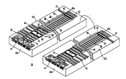
r~he mass *~ u~ ,uh I is . ' ' in a ' chip 23
15 as illustrated im Figure 2. In the exemplary ~11~ v . ' I, the chip 23 is about 20
mm long, 10 mm wide and 0.8 mm thick. This chip 23 comprises a substrate of
material forrned in two halves 25a and 25b which are joitled along
lly extending parting surfaces 27A and 27b. The two substrates halves
25a and 25b for~n at their ~arting surfaces Z7a arld 27b an elongated cavity 29.20 This cavity 29 has an inlet section 31, a gas ionizing section 33, a mass filter
section 35 and a detector section 37. A number of partitions 39 formed in the
substrate extend across the cavity 29 forming chambers 41. These chambers are
' by aligned al~ertures 43 in the partitions 39 in the half 25a which
defme the path of the gas through the cavity 29. The vacuum pump 15, shown in
25 Figure 1, is connected to each of the charnbers 41 through lateral passages 45
formed irl the r ~ ' v surfaces 27a and 27b. This v provides
,''' i pumpmg of the chambers 41 and makes it possible to achieve the
pressures required im the mass fiiter and detector sections with a miniature vacuum
pump. As mentioned previcusly, any collision between am ion and a gas molecule
will randomi~e the ion's trajectory reducing the desired ion current and raising the
b~.. h~ ' The mean free path is the average distance that a gas molecule trdvelsunder conditions of i . ,, and pressure before ~ -- v another gas
WO 96/16430 PCTIUS94/13509
1 81 8 ~ 6 -
molecule. The mean-free path of a gas molecule m air at ambient i l c is
about Icm at a pressure on the order of 10 mTorr.
The inlet section 31 of the cavity 29 is provided with a dust filter 47
which can be made of porous silicon or sintered n~etal. Tbe inlet section 31
5 includes several of the apertured partitions 39 and; therefore, several chambers 41.
The gas ionizing section 33 of the cavity 29 houses a gas ionizing
system 49 which includes a gas ionizer 51 and ionizer optics 53. The gas sample
drdwn into the mass ,~ .u~ Jh I consists of neutral atoms and molecules. To be
sensed, a fraction of these neutrals must be ionized. Different ionization schemes
10 exist, such as photo-ionization, field ionization or chemical ionization; however, the
most commonly used ionization technique in mass ~~ ,t,., and ~II~IIU~
is ionization by electronic impact. In this technique, an electron gun (e-gun)
accelerates electrons which bombard the gas molecules and ~ ively ionize
them.
15 ~ The most common electron emitter in mass ~I~LI~ uses
refractory metal wire which when heated undergoes thermionic electronic emission.
These can be scaled down usmg 1' ' ' ~Id~ to micron sized ~'
However, thermionic emitters require special coatings to rcsist oxidation and are
power hungry, but are capable of producmg relatively large amounts of electron
~Q current,.~ , ImA.
Due to the sensitivity of the detectors uscd in the subject s~LIugld~
to be discussed below, and to the higher gas pressure m the ionization section made
possible by the differential vacuum pumpmg, much smaller electron beam currents,about I ,uA are required of the e-gun. Two emitters developed by the assignee ofthe subject invention can meet this 1~ ,..i. The first is the field effect cold
cathode emitter which uses a sharpened point or edges to create a high electric field
region which enhances electron emission. Such cathodes have been tested up ~o
50,uA beam current, and are readily fabricated by semi-conductor ~
, One !'- ~ of field emission cold cathode is the tendency to foul
30 from: in the test gas, therefore, differential pumpmg of the cathode
would be required. The second e-gun scheme is the reverse bias p-n junction which
is less prone to fouling and is, therefore, the preferred electron emitter for the
WO 96116430 PCI-IUS94/13509
7 : 2 1 ~ 1 8 0 1
~u~llu~;.c.,uh of the inventian. The reverse bias p-n junction sends an electroncurrent racing through the solid state circuit. Near the surface, the very shallow
junction permits a fraction of a highest energy of electrons to escape into the
vacuum. Such small electrûn currents are required that a thin gold film will
5 produce the desired emissions over a long time.
The ion optics 53 comprise electrodes 55 on several of the apertured
partitions 39. The ion optics 53 accelerate the ions and collimate the ion beam for
. ' intû the mass filter 11.
The mass filtel I l is located at the mass filter section 35 of the cavity
10 29. The preferred ' ' of the invention uLilizes a permanent magnet 57
which reduces power, , - This permanent magnet 57 has upper and lower
pole pieces 57a and 57b, see Figure 3, which straddle the substrate halves 25a and
25b and produce a magnetic field which is ~ " ' to the path of the ions.
The orthogonal electric field for the Wien filter used in the preferred, L
15 of the mvention is produced by opposed electrodes 59 formed on the side walls 61
of the mass filter section 3S of the cavity 29. As shown in Figures 2 and 3,
additional pairs of opposed trimming electrodes 63 are spaced along the top and
bottom walls of the mass filter section 35 of the cavity 29. A spectrum of voltages
is applied to these additional electrodes to make the electric field between the20 electrodes 59 uniform. Thes~ additional electrodes 63 are made of _ ,
electrically conductive material such as gold so that they do not interfere with the
magnetic field produced by the permanent magnet 57. These electrodes 63 are
deposited on an insulating layer of silicon dioxide 64a and 64b lining the cavity 29.
As an alternative to the permament magnet 57, the magnetic field for
the ~nass filter 11 can be generated by a magnetic film 65 deposited on the insulating
silicon dioxide layers 64a an~ 64b on the top and bottom waUs of the mass filtersection 35 of the cavity 29 as shown in Figure 4. In this . ' ' t, the electric
field trirnmimg electrodes 63 ;Ire deposited on an insulating layer of silicon dioxide
66a and 66b covering the magnetic film 65.
;L . The ion deteclor 17 is a linear array 67 of detector elements 69
oriented in the dispersion plalle 71 (~ . to the planes of Figures 3 and 4)
at the end of the detfflor section 37 of the cavity 29. The exemplary array 67 has
WO 96/16430 PCI/US94/13509
ç ~ 1 8 -- 8 -
64 detector elements or channels 69. The detector elements 69 each include a
Faraday cage formed by a pair of converging electrodes 73a and 73b fornled on the
surfaces of a v-shaped groove 75 formed in the end of the cavity 29. The Faradaycages increase signal strength by gathering ions that might be slightly out of the
dispersion plane 71, through multiple collisions.
The electrodes 73a and 73b of the Faraday cage extend beyond the
end of the cavity 29 along the parting surfaces 27a and 27b of the substrate halves
29a and 29b. These electrodes 73a and 73b are plated onto the insulating layers 64a
and 64b of silicon dioxide formed in the two substrate halves 25a and 25b. The
IQ electrode 73b extends into a recess 79 in the insulating silicon dioYide layer 77b to
form a capacitor pad for a charge coupled device (CCD) or metal oY~ide
(MOS) switch device 81 formed in the substrate half 25b. The ions
are dispersed by the mass filter 11 in the dispersion plane 71 to strike a detector
element as .' ' by their mass/charge ratio. When the ion strikes the
15 electrode 73a or 73b of the detector element 69, its charge is li~P~I The
charge required to neutrali~e the ion is read out by the CCD or MOS 81.
Isolating electrodes 83a and 83b extend i .~ across the upper
and lower ~valls of the cavity 29 between the detector electrodes 73 and the
elfflrodes of the mass filter sfflion. These electrodes 83a and 83b are grounded to
20 isolate the detector elements from the fields of the mass filter. A sealant 85 fills the
recess 79 and joins the two substrate halves 25a and 25b.
Figure 5 shows the circuit: v for l~;r~Py~ operation of
an ion detector array 67. In this scheme, the ions are incident on one electrode of
the capacitors, Cs Of the detector elements 69. The ionic charge is neutrali~ed by
25 the sensor capacitor electrvdes 73b leaving behind a net positive charge on the
sensor capacitors, Cs~ The total ionic charge on each capacitor Cs is integratedover an integration period, for example, 90 msec. in the exemplary, I ' of
the invention. During this time, "i, ' switches 87l 6,l shown m Figure 5 are
im the off condition and are designed to provide very low leakage to improve the~Q sensitivity of detection. At the end of the integration reriod the multiplexer
switches are sequentially turned on to discharge the ' ' charge on the
WO 96/16430 PCT~US94/13509
- 9 - 2~ 818~
sensor capacitors onto the much larger gate . ~ of an cl~L., amplifier
FET 89. The change in gate voltage due to these additional charges is amplified
and converted to an output current signal by the ~I~LI, 89. To improve the
sensitivity of detection it is necessary to minimize the noise introduced by the5 ~' 89 ar~d the ~ ' switches 87 in the circuit. For this reason, P-
chalmel MOSFETs were chos( n for these devices since they have much lower noise
than N-channel devices. To further reduce noise and minimize the effect of
switcbing transients a techni4ue called Correlated Double Sampling (CDS) 91 is
used, to process the output current signal from the u l~llu,l,_t~,..
IQ The CDS scheme utili7es a four cycle operation for signal readout as
shown in the timing diagr~un of Figure 6. In this scheme the gate of the
ellU_IlUlll~,t~,l 89 is first reset to a reference voltage IVR by turnirlg a reset switch 93
on during a reset period. At the end of the reset period, the gate voltage of the
~1~1., 89 is slightly different from V~l due to noise and switching transients.
15 For this reason the output curr~nt of the ~l~u~..._t~.. 89 is measured during a clamp
period and stored in offchip capacitors. The next operation is to turn one of the
' . ' switches 87 on to discharge the mtegrated charge on the sensor capacitor
onto the ~ u..._t~. gate. The output current of the ' 89, which is
dependent on the amount of ch,~rge discharged into the gate, is then measured during
20 the sampling period. The difference in the output current values obtained in the
sampling and clamp periods i5 ,ululJulliullal to the integrated ionic charge which is
the desired signal. This four ~ ycle operation is then repeated for the remainder of
the array. The l-'rr _ pl~cedure used in CDS substantiaUy reduces switching
tlansient effects, reduces reset noise, and also redluces noise arising from the25 ~ , 89.
The various timing signals required for the detector array can be
generated with digital circuits 95 preferably made with CMOS to reduce power
~" . In the exemplary ' " of the mvention, dynamic shift registers
have been used to generate the ' . ' timing signals. Off-chip circuitry is used
30 to generate the remaining control signals such as the blooming control signal which
limits the amount of charge ~hich can reside on a sensor capacitor, so that small
wo 96/16430 2 1 8 1 8 0 1 PCT/USg4113509
1 0 -
signals on adjacent sensor capacitors can be determined without cross talk
;.... F~ from charges induced from high signal sensor capacitors.
A plan view of one ' ' of the linear detector array 67 is
shown in Figure 7. As can be seen from Figures 7 and 8, the Cr/Au ion sensor
metal 73b which forms onelhalf of the Faraday cage for each of the sensor elements
69 extends through via opening 97 in a dielectric layer 99 on the chip to contact an
aluminum metal lead 101 embedded in the substrate 103. As shown in Figures 7
and 9 lead 101 extends over a p+ implant region 105 and is sepa~ated therefrom by
a thin, such as 1,000-3,000 angstrom thick, dielectric layer 107. The lead 101
10 forms one plate, and the p+ implant 105 forms the other plate of tbe capacitor Cs
The p+ implant 105 is connected to ground through an aluminum ground contact
lead 109 which extends paraUel to the lead 101. The p+ implant 105 is formed in
the substrate 103 and is electricaUy comnected to the ground contact lead 109
through an opening in the dielectric layer 107. In the exen plary; ' ' of the
15 invention, the field oxide layer 99 is silicone dioxide about 8,000 angstroms thick.
As can be seen from Figure 7, aU of the ground contacts 109 from
each of the detector elements 69 are connected to a transverse grour~d lead 113
through via openings 115.
The aluminum lead 101 for each of the detector elements 69 extends
to and contacts a p+ implant 117 of the P-channel MOSFEI " . ' switch 87.
The gate electrode 119 of each of the switches 187 is connected to a lead 121 which
extends to the CMOS control circuit 95. The p+ implant regions 117 of all of theswitches 87 are connected by a common lead 123 to the reset switch 93 which is
also a P-channel MOSFET. The lead 123 is also connected to the gate of the
25 el~LlU~ l amplifier FET 89.
The n-weUs of all of the P-channel MOSFET "i ' switches 87
identifled by the reference character 125 are joined as shown in Figures 7 and 10
at one end. As shown im Figure 10, alummum contacts 127 are proYided at
openings 129 in the oxide layer 107 to reduce the electrical resistance across the
30 connected n-weUs. An n + layer improves electrical contact between the n-wells
125 and the alun~inum contacts 127. A lead 131 connected to the n-weUs carries
the blooming control signal.
WO 96116430 PCT/US94/13509
1 8 ~ ~
Figure 11 sho~s a modified; ' - of the detector array 67~.
In this array, the sensor electlodes 73~ of the Faraday cages are surrounded by a
grounded electrode 133 to provide better cha~mel separation. These electrodes 133
are grounded through the leacl 135 and provide a path to ground for the capacitor
5 ground electrodes 109 connecl~ed to the electrodes 133 through via 137.
While specific ' ' of the invention have been described in detail,
it will be ~ ' by those skilled in the art that various ~ and
alternatives to those details cauld be developed in light of the overall teachings of
the disclosure. Accordingly, the particular ~ disclosed are meant to be
10 illustrative only and not limiting as to the scope of invention ~hich is to be given
the full breadth of the append~d clairns and any and a~l ~ v ' thereof.