Language selection

Search

Patent 2181846 Summary

Third-party information liability

Some of the information on this Web page has been provided by external sources. The Government of Canada is not responsible for the accuracy, reliability or currency of the information supplied by external sources. Users wishing to rely upon this information should consult directly with the source of the information. Content provided by external sources is not subject to official languages, privacy and accessibility requirements.

Claims and Abstract availability

Any discrepancies in the text and image of the Claims and Abstract are due to differing posting times. Text of the Claims and Abstract are posted:

  • At the time the application is open to public inspection;
  • At the time of issue of the patent (grant).
(12) Patent: (11) CA 2181846
(54) English Title: INP/INGAAS MONOLITHIC INTEGRATED DEMULTIPLEXER, PHOTODETECTOR, AND HETEROJUNCTION BIPOLAR TRANSISTOR
(54) French Title: DEMULTIPLEXEUR, PHOTODETECTEUR ET TRANSISTOR BIPOLAIRE A HETEROJONCTION EN CIRCUIT INTEGRE MONOLITHIQUE INP/INGAAS
Status: Deemed expired
Bibliographic Data
(51) International Patent Classification (IPC):
  • H04J 14/02 (2006.01)
  • H01L 27/144 (2006.01)
  • H04B 10/148 (2006.01)
(72) Inventors :
  • CHANDRASEKHAR, S. (United States of America)
(73) Owners :
  • AT&T IPM CORP. (United States of America)
(71) Applicants :
(74) Agent: KIRBY EADES GALE BAKER
(74) Associate agent:
(45) Issued: 1999-03-30
(22) Filed Date: 1996-07-23
(41) Open to Public Inspection: 1997-02-15
Examination requested: 1996-07-23
Availability of licence: N/A
(25) Language of filing: English

Patent Cooperation Treaty (PCT): No

(30) Application Priority Data:
Application No. Country/Territory Date
514,707 United States of America 1995-08-14

Abstracts

English Abstract


The present invention relates to a monolithic integrated demultiplexing
photoreceiver (10) that is formed on a semi-insulating InP substrate(16). A
frequency routing device (11) is formed on the substrate and includes a first
plurality of InP/InGaAs semiconductor layers. At least one p-i-n photodiode
(12) is also formed on the substrate and includes a second plurality of
InP/InGaAs semiconductor layers. Additionally, at least one single
heterostructure bipolar transistor (18) is formed on the substrate and includes a
third plurality of InP/InGaAs semiconductor layers. At least one layer from
each of the first, second and third plurality of layers are substantially identical
to one another.


French Abstract

La présente invention porte sur un photorécepteur démultiplexeur intégré monolithique (10) formé sur un substrat semi-isolant d'InP (16). Un dispositif d'acheminement de signaux (11) est formé sur ce substrat et comprend une première pluralité de couches semi-conductrices d'InP/InGaAs. Une photodiode p-i-n (12) au moins est également formée sur le substrat et comprend une seconde pluralité de couches semi-conductrices d'InP/InGaAs. De plus, un transistor bipolaire à hétérostructure simple (18) au moins est formé sur le substrat et comprend une troisième pluralité de couches semi-conductrices d'InP/InGaAs. Trois couches au moins, appartenant chacune à une pluralité différente parmi les trois pluralités de couches, sont essentiellement identiques.

Claims

Note: Claims are shown in the official language in which they were submitted.


-6-


Claims:

1. A monolithic integrated demultiplexing photoreceiver
characterized by:
a semi-insulating InP substrate;
a frequency routing device formed on said substrate including
a first plurality of InP/InGaAs semiconductor layers;
at least one p-i-n photodiode formed on said substrate
including a second plurality of InP/InGaAs semiconductor layers;
at least one single heterostructure bipolar transistor formed on
said substrate including a third plurality of InP/InGaAs semiconductor layers,
at least one layer from each of said first, second and third plurality of layersbeing substantially identical to one another.

2. The photoreceiver of claim 1, further characterized in that said
second and third pluralities of semiconductor layers includes a common
InGaAs collector layer and a common InGaAs base layer.

3. The photoreceiver of claim 2, further characterized in that said
first, second and third plurality of layers includes a common n+ InGaAsP
layer serving as a waveguide core for said frequency routing device and as
an n-contact layer for said p-i-n photodiode and said single heterojunction
bipolar transistor.

4. The photoreceiver of claim 3, further characterized in that said
common n+ InGaAsP layer is disposed on an n- InP layer serving as a lower
cladding layer for said frequency routing device.

5. The photoreceiver of claim 2, further characterized in that said
common InGaAs collector layer is doped n-type and said common InGaAs
base layer is doped p-type.


-7-


6. The photoreceiver of claim 3, further characterized in that said
third plurality of layers includes an InP emitter layer disposed on said
common InGaAs base layer.

7. The photoreceiver of claim 4, further characterized in that said
third plurality of layers includes an InP emitter layer disposed on said
common InGaAs base layer.

8. The photoreceiver of claim 3, further characterized by an
electrically isolating region disposed in said common n+ InGaAsP layer
between said frequency routing device and said p-i-n photodiode.

9. The photoreceiver of claim 4, further characterized by an
electrically isolating region disposed in said common n+ InGaAsP layer
between said frequency routing device and said p-i-n photodiode.

10. The photoreceiver of claim 8, further characterized in that said
electrically isolating region comprises Fe implanted in said common n+
InGaAsP.

11. The photoreceiver of claim 6, further characterized in that said
third plurality of layers further includes an InGaAs emitter contact layer
disposed on said InP emitter layer.

12. The photoreceiver of claim 1, further characterized by a plurality
of single heterojunction bipolar transistors formed on said substrate, said
plurality of single heterojunction bipolar transistors being arranged in an
amplifier configuration.

13. The photoreceiver of claim 1, further characterized in that said
frequency routing device has a plurality of output waveguides and further
comprising a plurality of p-i-n photodiode and single heterojunction bipolar
transistor pairs formed on said substrate, each of said output waveguides

-8-


having associated therewith one of said p-i-n photodiode and single
heterojunction bipolar transistor pairs.

14. A method for fabricating a monolithic integrated demultiplexing
photoreceiver comprising the step of:
depositing on a semi-insulating InP substrate a first series of
layers forming a frequency routing device, said first series of layers including a
first plurality of InP/InGaAs semiconductor layers;
depositing a second series of layers that together with at least
one of said first plurality of layers forms a p-i-n photodiode and a single
heterostructure bipolar transistor.

15. The method of claim 14, characterized in that said at least one of
said first plurality of layers serves as a waveguide core layer for said frequency
routing device and as an n-contact layer for said p-i-n photodiode and said
single heterojunction bipolar transistor.

16. The method of claim 15, characterized in that the step of
depositing said first plurality of layers includes the steps of:
epitaxially growing a lower cladding layer, said waveguide core
layer, a stop etch layer, and a strip loading layer;
etching said strip loading layer to define a rib;
epitaxially growing an upper cladding layer over said rib.

17. The method of claim 16, characterized in that the step of
depositing said second series of layers includes the step of:
depositing a mask over said frequency routing device;
etching away said strip loading layer and upper cladding layer
from portions of said substrate not covered by said mask such that said layer
serving as said waveguide core layer is exposed;
epitaxially growing over said waveguide core layer a collector
layer, base layer, emitter layer and emitter contact layer;

-9-


etching said portions of said substrate not covered by said mask
to define said p-i-n photodiode and said single heterojunction bipolar transistor.

18. The method of claim 14, further characterized in that said second
series of semiconductor layers includes an InGaAs collector layer and an
InGaAs base layer

19. The method of claim 18, further characterized in that said first
plurality of layers includes an n+ InGaAsP layer serving as a waveguide core
for said frequency routing device and as an n-contact layer for said p-i-n
photodiode and said single heterojunction bipolar transistor.

20. The method of claim 19, further characterized in that said first
plurality of layers includes an n- InP layer serving as a lower cladding layer for
said frequency routing device and wherein said n+ InGaAsP layer is disposed
on said n- InP layer.

21. The method of claim 18, further characterized in that said
common InGaAs collector layer is doped n-type and said InGaAs base layer is
doped p-type.

22. The method of claim 19 further characterized by a step of
implanting an electrically isolating region in said n+ InGaAsP layer between
said frequency routing device and said p-i-n photodiode.

23. The photoreceiver of claim 1, characterized in that said frequency
routing device comprises:
a plurality of input waveguides;
a first free space region connected to the plurality of input
waveguides;
an optical grating connected to the first free space region and
comprising a plurality of unequal length waveguides;

-10-


a second free space region connected to the optical grating; and
a plurality of output waveguides connected to the second free space
region.

Description

Note: Descriptions are shown in the official language in which they were submitted.


- - 218~846
InP/lnGaAs MONOLITHIC INTEGRATED DEMULTIPLEXER,
PHOTODETECTOR, AND HETEROJUNCTION BIPOLAR TRANSISTOR
Technical Field
The present invention relates to semiconductor devices, and in
5 particular, to semiconductor devices having integrated electronic and photonic devices.
Backqround of the Invention
With the rapid development of lightwave communications, iow cost, high
perfommance optical receivers are needed for a variety of systems ~ 5-
10 Silica fibers in the long wavelength range (1.3 -1.6 microns) have relatively low
attenuation and aucoldi"yly, a high degree of interest has been generated by
integrated optical receivers which operate in this spectral range.
A monolithic pl~u~u,~ceiverthat integrates a pl~ulud~te:uLur and a
heterojunction bipolar transistor is disclosed in U.S. Patent No. 5,063,426.
15 While this configuration allows the photonics and ~lel,u~lics to be separately
optimized while Illcillldi,lillg materials cu,,,, ' "'.y, it fails to integrate a
demultiplexer, which is used in wavelength division multiplexed communication
systems to resolve the multiplexed channels prior to detection and
ar", ';'iCdliol1. The integration of the demultipiexing and detection functions
offer a number of advantages, including automatic optical alignment, reduced
number of required C~lll,uO~ , improved reliability and reduced cost.
Accordingly, it is desirable to provide a pl~ululH~ er that integrates a
pl lul~JrlHlH~,l JI, heterojunction bipolar transistor and a demultiplexer.
Summarv of the Invention
The present invention relates to a monolithic integrated demultiplexing
,ul ~JtUI H~eiver that is fommed on a semi insulating InP substrate. A frequencyrouting device is formed on the substrate and includes a first plurality of
InP/lnGaAs semiconductor layers. At least one p-i-n pl1uludiu~ is also fommed

- 21 8t 846
on the substrate and includes a second plurality of InPtlnGaAs semiconductor
layers. Additionally, at least one single heterostructure bipolar transistor is
formed on the substrate and includes a third plurality of InP/lnGaAs
semiconductor layers. At least one layer from each of the first, second and
S third plurality of layers are substantially identical to one another. In one
embodiment, this layer is a common n+ InGaAsP layer serving as the
waveguide core of the frequency routing device and as the n-contact layer for
both the p-i-n photodiode and single heterojunction bipolar transistor. The
common n+ InGaAsP layer may be disposed on an n InP layer serving as the
lO lower cladding layer of the frequency routing device.
Brief D~ i,Jti~l~ of the Drawinqs
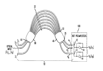
FIG. 1 shows a schematic diagram of a monolithic integrated
demultiplexing photoreceiver in accur.la~ ,ce with the present invention.
FIG. 2 ~ul~ dli~ ~"y depicts a cross-sectional view of the demultiplexing
15 ~l1utur~ceiver shown in FIG. 1.
FIG. 3 shows an exemplary amplifier circuit that may be used in the
present invention.
Detailed Dt:..il i"liol1
In a~,coldao~,e with the present invention, a monolithic integrated
20 demultiplexing photoreceiver cu,, ~,uli~il ,g a frequency routing device, a p-i-n
pl1u~udiûd~ and a heterostructure bipolar transistor (HBT) has been realized in
the InP/lnGaAs material system. As shown in FIG. 1, frequency routing device
1û contains a plurality of input waveguides 2j, i=1, 2, ..., N connected to the
input circle 95 of a free space region 98. An optical grating 32 extends from the
25 output circle 97 of the free space region 98 and is co""eu~d to an optical
grating 32. The optical grating 32 comprises a plurality of unequal length
waveguides which provides a pl~d~",lilled amount of path length difference
to optical signals plupaydlillg therein. The optical grating 32 is cu,,,~eule:d to
the input circle 33 of another free space region 46. The output circle 35 of the

' 218~846
free space region 46 is connected to a plurality of output waveguides 4k, k=1,
2, .,., N. The frequency routing device spectrally resolves a wavelength-
multiplexed signal appearing at any of its input waveguides by directing each
wavelength to a distinct output waveguide. Additional details conceming these
routing devices may be found in U.S. Patent Nos. 5,002,350 and 5,136,671, for
example.
An optical wavelength appearing on an output waveguide of the
frequency routing device 10 is detected and amplified by a photoreceiver 100
situated adjacent to the each output waveguide. That is, each output
10 waveguide of the frequency routing device 10 is A~so~i,.lH~i with a distinct
pl~ulu,Hceiver 100. Each pllu~urH~eiver 100 includes a p-i-n photodiode 12 and
an amplifier 14. The amplifier 14 comprises one or more HBTs.
In the present invention, the frequency routing device, p-i-n photodiode
and HBT have semiconductor layers selected from the InP/lnGaAs material
15 system which are grown over a semi-insulating InP substrate. Standard
rabli~dliol~ techniques including Il~ OIydl~i~i vapor phase epitaxy (MOVPE),
selective wet chemical etching, reactive ion etching, and contact metalization
are used to fabricate a device in accolddl1ce with the principles of the
invention. These ~d~liC~liul~ techniques are well-known to those persons of
20 ordinary skill in the art and, thus are not discussed in detail here.
FIG. 2 scllullldtic;31ly depicts a cross-sectional view of the monolithic
demultiplexing pl ,ulu, t:c~iver in accol .lallc6 with the principles of the invention.
The figure shows a single one of the waveguides 11 constituting the frequency
routing device, along with its ACSO,' ' i p-i-n photodiode 12 and HBT 18, The
25 exemplary ~IIIUO~ lll is grown on a Fe doped InP substrate 16. The
frequency routing device epilayers comprise lower cladding layer 1 (n InP),
waveguide core layer 2 (n+ InGaAsP), stop-etch layer 3 (InP), strip-loading
layer 4 (InGaAsP) and upper cladding layer 5 (n~ InP). It will be, UCoyl li~ed by
those of ordinary skill in the art that while the exemplary frequency routing

218~846
device i"~;ol ~ ol d~t~S a buried rib waveguide stnucture, any other type of
waveguide structure may be altematively used.
The p-i-n photodiode 12 comprises an absorber layer 6 (n~ InGaAs) and
p-contact layer 7 (p+ InGaAs). The absorber layer 6 is situated over the
S waveguide core layer 2, which serves as the n-contact layer of the p-i-n
photodiode 12. The HBT 18 is a single heterojunction bipolar transistor
(SHBT) in which the collector and base are formed from the same materials so
that a homojunction is formed Ill~l~b~ ". The SHBT 18 ~,ul"~.,i3es collector
layer 6, base layer 7, emitter layer 8 (n InP), and emitter contact layer 9 (n+ In
GaAs). Just as for the p-i-n ~JI ,u~,diode 12, the waveguide core layer 2 servesas the SHBT c u'- ~: '~f
The demultiplexing photoreceiver shown in FIG. 2 was fabricated in only
three epitaxial growth steps. In the first step, lower cladding layer 1,
waveguide core layer 2, stop etch layer 3 and strip loading layer 4 were
IS epitaxially grown on substrate 16. Wet chemical etching was then pel~ul,,,ed to
define the rib in the strip loading layer 4. In the second epitaxial growth step,
the upper cladding layer 5 was grown to bury the rib, culllpl~lil ,9 the buried-rib
waveguide structure. An SiO2 mask was next deposited over the cu" I~ lt lt,d
waveguide portion of the substrate constituting the frequency routing device so
~0 that strip loading layer 4 and upper cladding layer 5 could be etched away from
the ,t" "a;, Id~l of the substrate. With the Siû2 mask still in place, the p-i-nphotodiode 12 and SHBT 18 were fabricated in the third epitaxial growth step
by growing collector 6, base layer 7, emitter layer 8 and emitter contact layer 9.
Wet etching was then perfommed to realize the mesa structures of both the p-i-n
~ ulu~iocl~ 12 and SHBT 18. An t~ ,tli~lly isolating region 1û ~,~"".ri~i,ly Fe,for example, was implanted in the waveguide core layer 2 between the routing
device and p-i-n photodiode 12. The region 1û electrically isolates the p-i-n
pl1u~u.li~d,3s 12 from one another. If ~ t,i~ally isolating region 1û were not
present, the ~l ,uludi~des could electrically communicate with one another via
30 the waveguides of the frequency routing device. The i" I~ liu11 procedure

2181846
was pelrul,,,ed so that a highly resistive region 10 results without unduly
increasing scattering losses in the waveguides of the frequency routing device.
After i" ,~,ldr,ldtiù,, the device was annealed at 300C for 10 minutes.
Conventional metal contacts such as AuGe/Au and Au were deposited on the
flat surfaces of the mesas in order to provide ohmic contacts 22, 24, 26, 28 and30. Passivation of the resulting demultiplexing photoreceiver was
a.;~o,,,,ul;~lled by depositing polyimide over the entire device.
As detailed above, the invention advantageously integrates a frequency
routing device, p-i-n phulùdiode, and HBT by carefully selecting device
structures that are cul ",ud~i~le with one another so that at least one of the
layers in each device is also used in the other devices. Specifically, the
particular HBT that is selected is an SHBT so that the homojunction fommed by
its collector and base layers also serves as the absorber and p-contact layers
of the p-i-n photodiode. Consequently, both the SHBT and the p-i-n
pl1uL~diode may be formed during the same series of epitaxial depo~,it;~ns.
Moreover, by employing a frequency routing device having a core layer fommed
from an n+ doped material (rather than an undoped material, which is more
commonly used), the core layer also functions as the sll' ~ layer for both
the p-i-n p~1uludiod~ and the SHBT as well. The optical properties of the
20 ' waveguide are not suL,~Idr,lilly effected by using an n~ doped core material
rather than an undoped material
FIG. 3 shows one example of an amplifier circuit that may be used in the
present invention. The circuit has a transimpedance configuration cU",,uli~i"g
five SHBTs 30, 32, 34, 36, and 38 each having the structure shown in FIG. 2
and four resistors 31, 33, 35, and 37 for biasing and feedback. Additional
details cu, ,~6" ,;"9 the amplifier circuit may be found in U.S. Patent No.
5,063,426. One of ordinary skill in the art will recognize that the invention isnot limited to the particular amplifier configuration shown in FIG. 3. Rather, any
appropriate circuit may be chosen based on the particular A!; ' " ~ for which
it is intended.

Representative Drawing
A single figure which represents the drawing illustrating the invention.
Administrative Status

For a clearer understanding of the status of the application/patent presented on this page, the site Disclaimer , as well as the definitions for Patent , Administrative Status , Maintenance Fee  and Payment History  should be consulted.

Administrative Status

Title Date
Forecasted Issue Date 1999-03-30
(22) Filed 1996-07-23
Examination Requested 1996-07-23
(41) Open to Public Inspection 1997-02-15
(45) Issued 1999-03-30
Deemed Expired 2016-07-25

Abandonment History

There is no abandonment history.

Payment History

Fee Type Anniversary Year Due Date Amount Paid Paid Date
Application Fee $0.00 1996-07-23
Registration of a document - section 124 $0.00 1996-10-17
Maintenance Fee - Application - New Act 2 1998-07-23 $100.00 1998-06-29
Final Fee $300.00 1998-12-22
Expired 2019 - Filing an Amendment after allowance $200.00 1998-12-22
Maintenance Fee - Patent - New Act 3 1999-07-23 $100.00 1999-06-28
Maintenance Fee - Patent - New Act 4 2000-07-24 $100.00 2000-06-19
Maintenance Fee - Patent - New Act 5 2001-07-23 $150.00 2001-06-15
Maintenance Fee - Patent - New Act 6 2002-07-23 $150.00 2002-06-20
Maintenance Fee - Patent - New Act 7 2003-07-23 $150.00 2003-06-26
Maintenance Fee - Patent - New Act 8 2004-07-23 $200.00 2004-07-02
Maintenance Fee - Patent - New Act 9 2005-07-25 $200.00 2005-06-27
Maintenance Fee - Patent - New Act 10 2006-07-24 $250.00 2006-06-28
Maintenance Fee - Patent - New Act 11 2007-07-23 $250.00 2007-06-26
Maintenance Fee - Patent - New Act 12 2008-07-23 $250.00 2008-06-20
Maintenance Fee - Patent - New Act 13 2009-07-23 $250.00 2009-07-09
Maintenance Fee - Patent - New Act 14 2010-07-23 $250.00 2010-07-08
Maintenance Fee - Patent - New Act 15 2011-07-25 $450.00 2011-07-08
Maintenance Fee - Patent - New Act 16 2012-07-23 $450.00 2012-06-14
Maintenance Fee - Patent - New Act 17 2013-07-23 $450.00 2013-06-12
Maintenance Fee - Patent - New Act 18 2014-07-23 $450.00 2014-07-09
Owners on Record

Note: Records showing the ownership history in alphabetical order.

Current Owners on Record
AT&T IPM CORP.
Past Owners on Record
CHANDRASEKHAR, S.
Past Owners that do not appear in the "Owners on Record" listing will appear in other documentation within the application.
Documents

To view selected files, please enter reCAPTCHA code :


To view images, click a link in the Document Description column. To download the documents, select one or more checkboxes in the first column and then click the "Download Selected in PDF format (Zip Archive)" or the "Download Selected as Single PDF" button.

List of published and non-published patent-specific documents on the CPD .

If you have any difficulty accessing content, you can call the Client Service Centre at 1-866-997-1936 or send them an e-mail at CIPO Client Service Centre.


Document
Description 
Date
(yyyy-mm-dd) 
Number of pages   Size of Image (KB) 
Representative Drawing 1997-08-25 1 12
Cover Page 1996-10-30 1 12
Abstract 1996-10-30 1 15
Description 1996-10-30 5 174
Claims 1996-10-30 5 112
Drawings 1996-10-30 3 32
Claims 1998-12-22 5 134
Cover Page 1999-03-22 1 52
Representative Drawing 1999-03-22 1 9
Prosecution-Amendment 1999-01-18 1 1
Prosecution-Amendment 1998-12-22 3 120
Correspondence 1998-12-22 1 43
Correspondence 1999-04-20 1 42
Assignment 1996-07-23 6 218