Note: Descriptions are shown in the official language in which they were submitted.
WO 95/20195 PCr1AU94100247
21819~9
-- 1
FUNDS ~R~cAc~To~ DEVICE
Field of the Invention
Thi3 invention relates to a funds transaction
device and relate3 particularly but not exclusively to one
which may be mobile and operated via a bile t~l erhr~no
service .
De3criDtion of Prior Art
~"t1 ted teller r~~-h;~ - and l~FTPOS (l~lectronic
Fund8 Transfer Point of Sale) t~rm;n~lR have op~rPted for
many years. All current EFTPOS devices functio~ i~ the
same manner. An ~FTPOS card is ~swiped" through the device
to obtain account details, then an account type ~nd P.I.N.
(personal i~nt;f;~t;~n number) are entered an~d the
;nforr~t;~n ig gent to the banks for ~l~tr~n;~
authorisation. The afoLc ;nQd; - ti~n is ~n.~eeeed
through a PINpad which encrypts the P . I .N. details for data
security. The data is sent via a modem throù9h Rpec; ~
phone lines (leasea line8 that have ~ ~- c~"n~ti~n)
to a t ~n~-~t;on switchiD.~ network where lt is ~'switched"
through the correct bank's host ~ r to obtain bank
~uthorisation. In Au8tralia, the ~ystem v~ on
Australian ~elecom's ~rr~n$~n~ network.
The known systems offer msny di8advantaSre8. In
psrticular, the bility to have credit t ~ F~ from one
account to another, such as from a customer's account to a
~tore-holder'3 account who op~r~t~ the EFTPOS device is
currently limited to a fixed in-store situation and is
therefore not pr~t;~-~l for on-site tr~ Rp~op~e, market
store holder3 or the like as it is not ~-r-;hle to have the
n~c~r-ry ~rr~n$-~n-1 leased line3 at the variou3 3ites where
the tr~n~ct;~n is to occur for such persons.
Object and St~t~ of Invention
It is therefore an object of the present
invention to v~L~' the ~f~ n~d problem.
,hc efO e in ~cor~ nre with a first broad agpect
WO 95/20195 2 ~ 8 i 9 9 9 pcrlAu94loo247
-- 2 --
of the ~resent invention there _ay be ~rovided a funda
trAnaactir~n device for frAnaf~rring funds between one bank
account or credit facility and another bank account or
creait f acility
3aid device having:
l. A card reader device;
2. A PIN~ad device with an encr~tion system;
3. A modem device;
4. A c ;~at;nn interf~c~e device c~nn~ted
l O with the dem device;
5. An out~ut re~ort device;
6 . A c ; ~A~ n d~vice; 21nd
7. A central ~ -;n!J aevice;
_aid central proc~as;ng device (CP~l)5 interc-~ - .r~ ~ ;ng all of the devices l through 6, said
t;nn device, in use, being cr~nn~c~Ah3e with a
;cati~na network to connect to a host EFTPOS type
network c~nn~ t~9 with a bank or credit ~rt~h~
s~id CP~ bein~ ~LC__ ' to store -:L~L
20 identifying data of the owner/leasee of the ~ev~ ce and to
~ctivate said PIN~ad device 80 a uger can enter 1~ t; ~n
ViA said PIN~ad device such as, ~ccount type, ~Lccount
t ;nn type, trAna~rt;r~n amount, ~nd a PI~ nu~ber with
_aia PIN num~ber being encrypted by saia PIN~?ad aevice, and
25 wherein said PIN number is encrYpted and said user entered
~nforr-t;~n encry~?ted a8 a MessAge ~ h~nti~-At;on Code ~d
_tored by said CPTJ, activate a l~ at;~n cr~nn~ n via
said dem device and said ;nf~rfA~e device to connect with
the host EFTPOS device! ~nd trAn~---;t the stored user entered
30 data a3 well a_ tr~n~m; t the ~ L identifying data of
the owner/leasee of the device, 80 thAt funds can be
transferred from the user's bank account or credit or debit
card to the owner/ leasee ' 8 bank account or vice versa and
to ~rovide si51nals to the output rel?ort device confir_ing
35 the tr~naArt;~n or denial of the ~rAna~ n or other
;nfnrr--tir~n relating to the trAnaA~t;~ln
Most ~referably, the - rAt;~n device for
WO 95/20195 PCr/AU94/00247
2181q9q
-- 3 --
;cat;nn with the hoat EFTPOS device ia a mobile
t~ rh~n~ ayatem. It i3 particularly l?Lef6- d that a
bile tel e~hnn~ be built into the device . It ia
particularly prefell~d that the mobile t~larhnn~ is
5 ~ ;cAte~ to the purpoaes of c~ ;C~t;nSr with the host
13FTPOS network and ia without the uaual microphone or
earpiece Aa~ Ated with a to7~rhnn~ hand5et.
In A~cor~l~n~ e with a further broad aapect of the
present invention there may be provided a method of
10 ~ermittin~ a funds trAn~rtinn between one bank account,
and another bank account, aaid method com~riain~
storing account data o~ one party to the
trAnP~ tinn,
and atoring account data of the another party to
15 the trAnsaction by entering trJ~nP-~t;on particulara via a
PINpad device auch aa account type, account trnna-,Ct l~n
ty~pe, tranaaction amount, and PIN number e~cry-ptlng the P}N
number and atoring tho3e particulara aa an e ~; y~l.6d
~e~Page Authoriaation Code, . At;ng with a hoat
20 ~FTPOS type network and trAnPm;~-ting the 3tored le~aage
Au~:horiaation Code and data of the one party tr_..cr._r, In~J
funda from one party'3 bank account to the other party'a
bank account or vice veraa and ~nnf; rmi nSr via the output
report device the tran~action or denial of the t ; ~ln
a5 or other ;nforr-t;nn relating to the tr:~nP~ ~inn.
With auch a device a person effectin~ a
tr:~nPa~t;on need not be c~nn~t~d directly to a t97c-
~land line auch aa a Tran$end phone line which i3 uaually
not available in per~on'~ home~ where tradea peo~le may
30 require to make a trAnaA~ t;nn or at market atall ln-~t;nn~
where market atall holdera or o~rAtnr~ require to make a
transaction .
srief Deacril?tion of the Drawinga
In order that the invention cAn be re clearly
35 aacertained, an exam~ple of a pre~er.~d ~ will now
be (~e-a~r;h.o~l with reference to the A _ ying l~rAw;
wherein:
WO9S/20195 2 t 8 ~ 999 PCT/AU94100247
-- 4 --
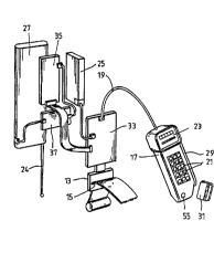
Figure 1 is a front isometric view of a _obile
funds transAction device fitted in ide a carry-bag. The
c~lrry b~g i8 shown open.
Figure 2 is a front ;- ' ric view of the device
5removed f rom the c_rry-bA g .
Figure 3 i-o a ~AL t;c view of the ;nt~rn~
' ry of the device;
Figure 4 is A block circuit diagr_m of the
device;
Figures 5A, 5B and 5C are detA; l e~ circuit
~'I;A5rrAma of _ central procegging unit circuit board used in
the device;
Figure~ 6A _nd 6B show tAblea of ~ _ ' types
and values in the circuitry shown in Figures 5A _nd 5B;
Figures 7A to 7F Are flow ~Ag Ame~ showing
fl~n~t;nnAl;ty of the software in the central rroces~;
unit circuit board.
Referring now to Figures 1 _nd 2, there iô 5hOWll
a mobile funds t An~ t I ~n device 1. The device 1 i3
20 ~ to fit within a carry-case 3. The carry-ca~e mAy
have _ olln~ r strap 5 and a cover or lid 7 which mAy be
retained relative to the case 1 to close the ca~e 1 by ~
s-~;t~hle fAot~n;nsr meA~ 9. The device 1 has _ housing 11
which ~l~ntA Ino the e~ectron;c circuity _or the device 1.
25 An out~ut report device 13 ln the form of _ printer i~
mounted on the housing 11 Ag shown. The output report
device 13 has An output ~lot 15 though which p_per can
issue providing a report on the t_ ct;~n which has
o~ cl or other ;nf~ ti~n rel~ting to the trAn~lAct;on.
30 A PINpad device 17 connects with the circuitry within the
housing 1 by means o~f a cable 19. mhe PINpad device has a
series of lcey pad3 21 by which a user may enter trAn~ n
particulars and it also has a visual display 23 through
whlch -~es~.cf~ or instructionO may be given. The PINpad
35device 17 also has a card 310t 29 in which _ user's card 31
may be swired in order to obtain particulars from the
user~ g card . A card reader device within the card slot 29
Wo 9512019~ PCr/AU94100247
2181999
-- 5 --
18 provided within the PINpaa device 17 80 as to r~ad
particular3 from the user's card 31 swiped through the card
slot 29. The housin~ 11 contains a a~ ca~ na device
in the orm of a mobile ~el Orh~ln~ system 27 as will be
5 o~lA;nod hereinafter. An aerial 24 extends from the
hous ing 1.
The housing 1, output report device 13, PINpad
device 17 and mobile phone 27 are gon~rA11y rectAngulAr in
shape and the PINpad device 17 can fit to the housing 11 80
that it is gon~-rAl ly occupying the available space on a
front face of the hou8ing which is not covered by the
output report device 13. A battery compartment 25 is
provided at the side of the housing 11 and may, in fact,
form an ;nl egr~1 part of the _ousing 11. Thu~, it can be
seen that the device 1 has the same general 8ize ~8 a
bile tP1erh~no 27 except that it is z~nor~lly thicker to
a~ e its own ;ntorn~1 central proc~s~ng unit
circuity, the output report device 13 and the PINl?ad device
17 . The PINl?ad device 17 is removable f or easy access by
users.
Figure 3 ~hows the a~ ~. of the various
c _ y within the housing 11. Thus, like ~ g
to those shown in Figures 1 ~nd 2 have been provided with
the same ~ 'cAl A~ig"n~ n~. The ~;rc~;try within the
housing 11 ;nrl~ a central ~ ~;n9 unit (CP~) board
33 havin~ an E13PROM nornory c~ ~_L~ therewith, a modem 35,
and an interface 37. Preferably the b~ttery 25 i~ an
gA~te f lat batterY .
Figure 4 shows the block circuit diagram of the
device with the printer 13, PINpad 17 and mobile phone 27
all int~ra., e~ Led with a central ~roco~;ng unit 39
forming part of the central proco~ing unit board 33. The
central proces~;n;r unit 39 has an EEPRO~ memory device 49
c~n"o~-t~ll therewith. The central proc~;ng unit 39 also
has c~nnocted to it a clock 41, a print ariver circuit 43,
a printer voltasJe re~1Ator circuit 45, a power control
switch 47, the main power battery 25 and a EEPRO~ chip 49.
_ _ _ _ _ _ _ _ _ _ _ .
WO 95/20195 2 1 8 1 9 9 9 PCr/AU94/00247
-- 6 --
The EEPR0~ chip 49 is provided to store certain info~-tinn
in memory in the CPU 39. The CPIJ 39 also haE a voltage
rogulator circuit 51, a modem 35 and a handset interface 53
cnnn~cted therewith and is also provided with a ~ArAllel to
5 serial interface 55 which converts ~ArAllel data to serial
data for f-rs~nF...; n5inn over the modem 35 and bile phone
27. It also permits data from the PINpad to be transferred
to and from the CP~ 39.
The mobile phone 27 may be any commercially
10 available mobile phone such a~ Motorola type 3194 cellular
phone. The dem 35 may be any su; t~hle commercially
available modem such as modem type ICM ~ l; oA by r~anksia
~hnnl~ ;on of 205/83 Longveville Road, rane Cove, New
80uth Wales, Australia. The PINpad 17 may be ~ny suitable
~ y available PINpad device with encry~tion
circuitry, display 23 and cara slot 29 with E~;t~hle card
re~der, such as one r^-n~f~ t~red by Tr~c Systems Australi~
of 1/61 Lawrence Drive, Neran~ on~lAnA, ~-n~rAl;A and
~ola under model TSP021. The out~ut report device may be a
~ Ahle printer such a~ model M-180 ~: ~d by Seiko
Epson Corpor~t;nn The handset ;ntcrf~r-e 53 m~y be a
suitahle ~ntorf~-e such as one sold by l~otorola and useable
for modem cnnn~c~;nn with a mobile or other ~ nn
device .
The funds ~rJ~nnrct;on device 1 h~s the CP~ board
33 Duitably prv~ -1 to initi~te the no~orr.ry l?-v~ .s
for the funas tr~nsfer, beforo, during and after c r~nn~ct~on
with a host funds t ~DLeI network. Such ; ,.~t; nn may
be by the mobile phone 27 or by other ~ ; ~A~; nn means .
In use, the device 1 is activated ~o the user~
card 31 can be swiped through the card slot 29 ~o that
account details on the card 31 can be read by the card
reader device. The CP~ board 33 then ;nA;~st~ via the
dis~?lay 23 that the user may manually enter their account
type, account tra~action required, and amount of
tr~nnA~t;nn, and the personal ;~ n~;f;cat;nn number (PIN)
via the key-pads 21. The PIN number is encrypted from t;he
WO9S/20195 PCr/AU94/00247
2 1 ~ ~ 9q9
-- 7
PINpad and with the other non encrypSed user entered data
i8 sent back to the PINpad 17 from ~n~Ar~ulAtinSr of the
data into an encrypted MAC (Messase A~h~nti~Ation Code) or
the like as required by Augtralian Standard 2805.3 via the
5 ;nt.~rnAl encryption circuits within the PINpad device 17.
The CP~ 1 then store~ the MAC within the EEPROM memory
chip. This ;nforr~t;~n is retained ln an encrypted form.
The CPIJ 33 then ~n;~;At~ a ~l;All;ng sequence via the modem
35 to effect ~ ;~A~ n with the hoat EFTPOS network.
10 Thi3, in turn, activates the mobile phone 27 to make the
n~ gAry ~l;All;n5r ~mnn~rt;nn~. The handset ;n~PrfAre 53
enables the data to be converted to appropriate signals for
the bile phone and also Allows for signals received by
the mobile phone to be approprlately converted to be fed
15 through the modem and p..~eA~e~ by the CP~T. When
~ nn~ n i8 made wlth the host ~3FTPOS network and any
particular bank required for the t r~n~-ctl~n to occur, the
~r~n~2Artlrm details are ~; ~p~trh~ ;nrlv~'l;ng the
owner/leasee's particulArs. The transaction request from
20 the device 1 ls then 5)ro~ ' by the bank and a reply
g~ln~rAte~ and ;r~ted back to device 1. The CP~ 33
receive~ that reply and an appropriate recei~t ia go~n~rAte~
through the output re~ort device 13 . The output f rom the
output rel?ort device 13 may be a receipt or a message
25 ~tating f;nAn~Al instit~t;~n rejection or other
inforr-ti~n. The printing of the report by the output
report device 13 may be elther whll~t the devlce 1 is
rmnnC~rted wlth the ho8t EFTPOS network or after t~rm;nAt;~n
of C~nn~ct; ~n,
The central pro~ ;ng unit 33 ig pre-p~
f or f our dif f erent receipt types f rom the output report
device 13. These are as followa:
1. Debit ~approval - statln~ card number, account
type and amount of transfer;
2. Credit Approval - aa in 1. but alao requiring
si~nAt~re on receipt;
3. Denial of the ~r~^n~ct;nn - lltating f;nAnr;Al
Wo 95l20195 pcrlAu94loo247
2181999
-- 8 --
institution re~ection;
4. Can~t Connect - statin~^, there is ~ problem
c-^nn-~^t; "g with eithQr the host EFTrOS device or
the tr~n-^A-^t;~^n switching network Duch as the
S bile tel ~rh~^n- service .
Once the appropriate mcssa~^~e has been ~rovAded by
the output device 13 or display 23, the CPIJ 33 will be
' to de-activate the circuitry u~til it i8 Aurther
Dwitched on for a subsesluent ~ ^t;-^n
The CP~r 33 may be suitnbly pr.__ - ' to ^tore
trAnAA-^t;~^n amounts so that the - _I~L owner/leasee of
the device 1 can per;-^A~^Ally print a journAAl/result for
administrAAtion purpo~es.
The t^l~rh~^n~ numbers for ^nnnD-^ting with the
15 EF~POS fun~Ag trAn~-~At;~A~n network may be m^nually pre-set in
thQ memory of the CPl~ 33 by the .iL~L owner/leasee or
may be ~ '^i into either the CP~ or, alternatively, the
mobile phone 27 at the time of ~~-^t~^e. The EEPRO!I
chip 49 ia providea to hold any volatile deta~ls in memory
20 in CP~r 33. The battery 25 mPAy typically be ~ recharge_ble
battery providing g--ff~ nt capacity to operate the device
1. A c-^nn--^t ~ ^n may be provided to perm~ t char~ing of the
battery 25 from either mainD or _rom a cAr battery. A plu"^,~
connection (not shown) may also be provided to permit
25 _Yt_rnAl power to be ~ ,ppl;~A to operate the device i~
n~c~ArAry. A t91erhnn_ ~lug socket may be provided to
permit direct c-^nno^t; ~^n to n public service t^l ~rh-^n-
network in ereaD where the mobile phone may not operate.
In this way, the device 1 m~y be c~^nn-~^ted with a host
30 EF~I!POS network via the normal public 3ervice t-lerh^
network rather thnn by the mobile phone 27.
The PIRpad device 17 will ac~u; re the trAn^~^t; ~^n
data from the user as follows:
An initial swipe o~ the user~s credit/debit card
35 may activate the circuitry in the CPU _or subse~luent
fl~n-^t;-^n~ of the device 1. Account details can be acc,uired
from the user's credit/debit card and also the eYpiry date.
W0 95/20195 ~ I 8 ~ 9 9 9 PCr/AU94100247
The rer~onal identification number can be ;nr~ltted throu~h
the key ~ad3 21. The amount of the trana--t;~n can al_o be
;~r~tt~d throus~h the key pada 21. The account type can
also be inputted throuSrh the key pads 21. The account type
5 might be cheque, ~avin5rs or other account. The account
t~Ana~t;~n may be credit or debit. The n~c~a~ry ;nrutted
;nfnrl-~t~n i~3 encrypted by the PINpad device 17 in
A~c~rAnn~e with the Australi n standard AS2805-3 rreviou_lY
referred to. The ~ owner/leasee of the device l can
lO have hi~ account detail_ or other detail suitably stored
in the memory of the central rroc~aa;ng unit 33. This
account inf~~ti~n need not be encrypted. A routine may
be provided in the p~_ 'n!J of the device 1 for the
merchant owner/leasee to in~ut hi5 account ;nfo~-t;~n into
15 the memory in the centrAl proces~in!J unit 33. This
;nf~l_-t~n can be ret~ined for t~na~;aai~n with each
transaction. In ~n ~lt^~n~t;ve ~ , the ~;La~L
owner/le~ee may h~ve ~n account c~rd which must ~luo be
swiped throuSrh the card slot 29 to extract the
20 owner/leasee's account p~rt;~ . If the
owner/le~see~s account particul~rs ~re obt~ined in thia
way, then the ; - r _; rln may be encrypted by the
encryption circuitry r~a;~l~nt in the PINpad device 17.
ReferrinSr now to the ~tn; 1 ~d circuit diagram of
25 Figures 5A, 5B, and 5C~ and to the _ y ~A~nt;f;~fl in
the ~ ~h~d~ 1 e of Figures 6A and 6B it can be seen that the
battery 25 is arran~ed to make electrical connection with
the circuitry throu~h a 1 At~h;n~ relay switch 82 . The
lAt~h;n~ relay switch S2 is, in turn, activated by
30 operati~n of a " n~ily on" switch Sl. The switch S2
i~ shown in the power on ~ :~it;~n for taking power from the
battery 25. ~ transistor Tl i8 cnnn~cted with ~11 and can
rrovide drop out of the l;~t"h~nSJ relay S2 80 that when a
si5~nal iB 8~r~ d to transistor Tl identifying thAt the
35 tr~na~ n has been completed, it nvt~ t;r~lly turn_ off
the l~t~-h;n~J relay S2 to ~ the battery.
The circuitry show~ an error ;n~;~nt;ng LlZD diode
Wo 95120195 PCr/Au94loo247
2181999
-- 10 --
D1 which i~ coloured red. The CPIl 33 irl ArrAnge~ to
activate D1 if a major f~ult occur~ with the fllnrtinnAl;ty
of the device, thu3 requiring re~air. A11 other error3 are
dis~layed on the PIN~ad 17.
The memory in the CPIJ 33 is ~?referably
~nrt;t;~n~cl to ~tore ~everal alternative EFTPOS network
tel~rhrn~ number~, and wherein the ~rogram is ArrAnSr~cl to
attempt to make rr~nnPrt; rn on one number ana i_ th~t is
l~nclvcr~ fu1 to attem~t to make cnnnc~cti~n on ~nother of
the numbers without intervention by the user.
The circuitry should otherwise be sel~-
tory to an electronics engine~r.
Referring now to Figures 7A, 7B and 7C there i~
shown n ~rogram f low-~liagram o~ ; n; n~ the E e ~ ;.. of
15 events for a trAno- ; nn . The diagr~m is self -~l AnAtory.
It should be a~reciated thAt many - ';f;cz~t;
m y be made to the l?resent invention AE woula be a~ rent
to ~ersong skilled in the banking and/or EFTPOS trnnC~ n
arts. For ex~le, it may be A~irAhle for commercial
m-n~fJ~rt--ring ~-n~ ' to place the CP~, modem,
~n~rfAre, battery voltage controller and ~?rinter card on a
single circuit board. Also, the swiving of the user'~ card
through the slot 29 may not ~ctivate the switch Sl which
arnn~c~ the battery 25 with the CP~ circuit 33. A switch
S1 which ig A;A~ ~;rAlly shown a8 ~in 55 in Figures 1
through 3 may be used 80 t_nt the device can be manually
switched on.
Further, inf-tead o_ the device Orc~rslt; nsr by a
te~ erhr~n~ - ; ~At; r~n link with the host EFTPOS network
it may operate via any suitable ~ ;c~t;r~n~ link which
ref~ults in the device not being 1;= ~ y ~_ysical~y
electrically connected therewith such as by the usual
$~nA lines ~;)reviously referred to.
These and other '; fi~Ati--n~ may be made without
35 departing from the ambit of the invention, the nature of
which is to be APt~rm;n~d _rom the foregoing descri~tion.