Note: Descriptions are shown in the official language in which they were submitted.
W O 95120341 ~ ~ pCTJUS94104931
-1-
METHOD AND APPARATOS FOR CONTROLLING
AN ELE~L:TRO-OPTICAL 86PITCH
C GROtINp OF TH ~. rt~E~ION
Field of Invention
This invention relates to electro-optical
switches and more specifically to a system for
controlling the voltage switching levels of an electro-
opti.cal switch array.
DescrsDtion of +t,p a ~ + a r
Optical switch arrays are used in many
different applications when it is desired to multiplex
an optical signal along multiple paths. For example,
it is known to use optical switch arrays in multiple-
ring fiber-optic gyro (FOG) systems to direct the
optical signal emitted from a single source to multiple
rings and from the rings to a detector. Such arrays
are reconfigured periodically by the selective
application of electrical signals.
A FOG system is used to sense rotation of a
vehicle (e.g., a spacecraft) about one or more axes of
rotation, and outputs from the FOG system are used to
provide navigation and flight control information for
the vehicle. A typical FOG includes a laser
source
providing an optical signal and a mufti-turn coil of
optical fiber referred to as a fiber-optic ring. The
optical signal is first applied to an optical beam
splitter/combiner which provides two identical optical
output signals, each o which .is applied to one end of
the fiber-optic ring. The two signals travel through
the ring in opposite directions and are recombined at
the beam splitter/combi.ner. Any rotation of the fiber-
CA 02182033 2001-02-06
-2-
optic ring about its wound or longitudinal axis will
result in a phase shift of the signals traveling
through the ring. This phase shift is known as the
Sagnac effect phase shift and is detected by analysis
of the recombined signal from the splitter/combiner
that is applied to an output detector.
A particular implementation of a FOG
incorporating an optical switch array is described in
U.S. Patent No. 4,828,389 to Gubbins et al. issued May
9, 1989.
The FOG described in that patent comprises three fiber-
optic rings oriented along orthogonal axes
representative of axes of rotation of the vehicle in
which the FOG is used. In that arrangement, light from
a single optical source is transmitted to a multi-port
optical switch array which transmits the signal to the
three separate rings, via separate beam splitters/
combiners, on a time-shared basis. The optical switch
array further functions to transmit the recombined
signals on a time-shared basis from the three rings to
a single optical detector.
The optical switch array described in the
above-noted patent comprises three switching stages
interconnected by optical channel waveguides. Each
switching stage comprises a bi-directional electro-
optical switch having two pairs of optical ports and
two pairs of electrodes by which control voltages may
be applied to the switch. The switches may be
fabricated from a crystalline material, such as lithium
niobate (LiNbo3), the index of refraction of which
changes as a voitage.signal is applied to the crystal.
The optical channel waveguides may be formed in the
crystalline material by indifusion of a dopant such as
WO15/20301 ~~,~ PCTIUS94l00931
-3-
titanium. By the proper application of appropriate
voltage control signals to the electrodes, each switch
may be set to a "cross" state in which a light beam is
deflected in the switch, and a "bar" state in which the
light beam is passed through the element without
deflection. By selective application of control
signals, controlling the cross and bar states of the
individual switches, it is possible to transmit optical
signals between opti~~al ports of the switching array in
each of a plurality of time slots. In the arrangement
described in the Gubbins et al. patent, two separate
optical paths are established in the switch array, in
each time slot. One path allows far the transmission
of a signal from a laser source to one of the fiber-
optic rings and the other path allows for the
transmission of a re<:ombined signal from another of the
rings to the output detector, in the same time slot.
Since each stage of the switch array comprises two
electrode pairs, six separate voltages must be applied
to a three-stage array in each time slot. Since each
switch may be placed in either the cross state or bar
' state, twelve different control voltages must be
available for control of the three-stage switch array.
The application of voltage signals to the
electrodes results in the establishment of electric
fields which create the bar and cross states within the
switch. The magnitude of an applied voltage at which
an electro-optical switch assumes the bar state or the
cross state is a function of the physical
characteristics of the crystal element and may change
with changes in environmental conditions, such as
temperature, and other changing conditions such as
charge migration and device life. :Ct has been
1VU 95!2(1301 ~ ~ ~ ~ ~ ~ ,~ PCT/IJS941pp931
-4-
recognized that the application of a voltage signal of
improper magnitude for either the cross state or the
bar state may cause an optical signal to be partially
blocked or misdirected. This phenomenon, referred to ,
as "leakage," may result in a reduced magnitude or
erroneous output signal from the switch and ultimately
in erroneous flight control information. It is
therefore desireable to minimize such leakage.
SUMMARY OF THE INVENTION
i0 These and other problems of the prior art are
overcome in accordance with the principles of this
invention in which optical leakage in an electro-
optical switch array, controlled by electrical control
signals, is minimized by detecting a measure of optical
Z5 output from the switch array in response to the
application of control signals of a predetermined
magnitude, modifying the magnitude of the control
signals and comparing optical output detected in
response to the application of the modified control
20 signals with the output value detected prior to the
modification. Thereafter the magnitude of the control
signals are set equal to the value of the control.
signals which provides the better output value. In one
particular embodiment of the invention, a plurality of
25 samples of output signal values are taken in response
to the application of control signals of the
predetermined magnitude. Additional samples are taken
in response to the application of the modified
magnitude control signals and accumulated sample values
30 axe compared in order to avoid adjustment to control
signals in response to short duration variations.
R'O 95120301 ~~ pCT/US94100931
-5-
According to one aspect of the invention, the
magnitude of one of the two control signals for a
selected one of the switches is first modified by
adding a predefined incremental value to the
predetermined magnitude for that control signal and
output signal samples are detected and corresponding
samgle values are stored. Thereafter, the other of the
two control signals for the selected switch is modified
by adding a predefined increment to the magnitude for
the other control signal and output samples are again
detected and corresponding sample values are stored.
The output signal values obtained at the modified
control signal magnitudes are examined and a
determination is made as to the magnitude of the
difference between the values of the output signal at
the original predetex~ined magnitude of the control
signals and at the modified magnitude of the control
signals. Further modification of the control signals
is made only if a significant change in output signal
value is detected.
In accordance with another aspect of the
invention, the magnitude of control signals is first
varied by a predetermined amount and values
corresponding to output samples are recorded as
representing points on a leakage curve for the switch
array. A gradient vector of the leakage curve is
computed as a function of the control signal magnitudes
and further samples of optical output signals are
collected at the point on the leakage curve represented
by newly computed values of control signal magnitudes.
New control signal magnitude values are computed
repeatedly until the optical output shows no further
significant improvement over a prior. reading. The
W'095120301 ~~'7.~-~ PCT/US9.llt1(1931
-6-
signal magnitude values providing a less than
significant change are used in deriving the magnitudes
of the control signals for subsequent application to
the selected switch.
In accordance with a particular aspect of the
invention, the magnitudes of the control signals are
selectively incremented by values computed by
multiplying predetermined incremental values by a
selected multiplier and the further step of
periodically incrementing this selected multiplier and
repeatedly collecting additional samples until the
difference between successively collected samples is
less than a predetermined threshold value and the
further step of adjusting incremental control signal
values as a function of the selected multiplier.
In accordance with one specific embodiment of
the invention, an optical switch array is provided with
a leakage detection output port and the magnitudes of
the control signals supplied to the switching array are
modified to minimize the optical output at the leakage
detected port.
In accordance with another aspect of the
invention, optical samples are taken from a primary
optical output port of the switch array and the
magnitudes of control signals are adjusted to maximize
optical output at the primary output port.
Advantageously, in a system in accordance
with the principles of this invention, optical leakage
in an electro-optical switch is minimized by
periodically varying the magnitude of the control
signals to provide minimum leakage values and without
interruption of normal switch operations.
CA 02182033 2001-03-15
64159-1517
7
In accordance with one aspect of the invention, an
optical switching system comprises an optical leakage detector
connected to an electro-optical switch array and system control
circuitry responsive to optical leakage output signals to
adjust the magnitude of control signals applied to the electro-
optical switch array.
In one specific embodiment of the invention, a filter
circuit is connected between the optical leakage detector and
the control circuitry. The filter circuit filters electrical
signals of greater than a predetermined frequency from
electrical output signals generated by the leakage detector.
In a further specific embodiment of the invention, the control
signals for an electro-optical switch are generated from a
first signal source element generating output signals of a
fixed magnitude and a second source element generating signals
of a second variable magnitude. The variable magnitude is
controlled by the control circuitry of the system and may be
adjusted from time to time in response to electrical output
signals representative of optical leakage.
In accordance with the present invention, there is
provided a method of optimizing an optical signal in an
electro-optical switch array having a plurality of input and
output ports including an optical output signal detection port
and comprising a plurality of electro-optical switches
responsive to control signals to selectively transmit optical
signals among the access ports, the method comprising the steps
of: applying an optical input signal to one of the input ports;
selectively applying control signals of differing magnitudes to
the switches; detecting optical output signals from the
detection port and after application of each of the control
signals; storing signal values representative of the detected
optical output signals; defining a preferred signal value for
CA 02182033 2001-03-15
64159-1517
7a
optical output signals and comparing the stored signal values
to the preferred value; selecting a control signal magnitude
substantially equal to the magnitude of applied control signals
resulting in optical output signal levels most nearly equal to
the preferred value; and subsequently applying control signals
of the selected magnitude.
In accordance with the present invention, there is
further provided a method of optimizing an optical signal in an
electro-optical switch array having a plurality of switch
access ports and comprising a plurality of switches optically
connected to the access ports, each of the switches responsive
to control signals to selectively transmit optical signals
among the access ports, the method comprising the steps of:
applying an optical input signal to one of the switch access
ports; selectively applying control signals to each of the
switches, each of the control signals having a predetermined
magnitude; detecting a first optical output sample from an
other of the switch access ports and storing a signal value
representative of the first sample; selecting one of the
switches; modifying the magnitude of control signals for the
selected switch by a predetermined value and applying the
control signals of the modified magnitude to the selected
switch; detecting a second optical output sample from the other
of the access ports and storing a signal value representative
of the second sample; computing of the difference between the
stored signal values representative of the first and second
samples; adjusting the magnitude of control signals for the
selected switch by an incremental value proportional to the
difference between the stored signal values of the first and
second samples.
In accordance with the present invention, there is
further provided an optical switching system comprising: an
electro-optical switch array comprising a plurality of switch
CA 02182033 2001-03-15
64159-1517
7b
access ports and an optical leakage detection port, the switch
array further comprising a plurality of switching elements each
responsive to electrical control signals of a first type to
assume a first operational state and responsive to control
signals of a second type to assume a second operational state;
an optical leakage detector connected to the optical port for
generating electrical output signals representative of optical
leakage in the switch array; and control circuitry connected to
the switch array and the detector and operative to selectively
apply electrical control signals of the first type and the
second type and of predetermined magnitudes to the switch
array, the control circuitry responsive to the electrical
output signal representative of optical leakage to adjust the
magnitudes of the controlled signals to reduce optical leakage
in the switch array.
BRIEF DESCRIPTION OF THE DRAWINGS
The invention will now be described with reference to
the drawings in which:
FIG. 1 is a block diagram of a fiber-optic gyro
system which incorporates the principles of the invention;
FIG. 2 is a block diagram of the electro-optical
switch array illustrated in FIG. 1;
FIG. 3 is a block diagram of the switching voltage
control circuitry of FIG. l;
wo osr2o3o1
PCTIUS9.tA)0931
_g-
FIG. 4 through 7 are flow charts illustrating
the process for adjusting control voltages for the -
electro-optical switch array of FIG. 1: and
FIG. 8 is a_diagrammatic plot of leakage ,
values.
tfETAILED DESCRIPTION
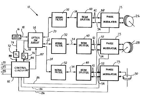
FIG. 1 illustrates an exemplary embodiment of
a fiber-optic gyro system (FOG) 10 including three
fiber-optic rings 26, 28 and 30, optically connected to
a light source 16, a primary photodetector 72, and a
secondary leakage detector 76 via an electro-optical
switch array 14. The light source 16 may be a standard
laser light source providing an optical signal S which
is transmitted on optical conductor 18 and through
optical switch array 14 to three optical conductors 20,
22 and 24 in a timed sequence. The optical conductor
is connected through a modal filter 32, optical
conductor 34, a beam splatter 40 and an optical path 42
via a phase modulator 73 to fiber-optic ring 26. In a
20 similar fashion, optical conductor 22 is optically
connected to fiber ring 28, and optical conductor 24 is
optically connected to fiber ring 30, through a modal
filter 32, an optical conductor 34, a beam sputter 40,
an optical path 42 and a phase modulator 73. The modal
filters 32, beam splatters 40 and phase modulators 73
are well-known devices and their operation is discussed
in detail in the above-noted Gubbins et al. patent,
which is incorporated by reference herein.
Briefly summarized, the operation of the FOG
10 is generally as follows: an optical signal S is
generated by the light source 16 and transmitted via
optical conductor 18 to the optical switch array 14.
yfO95I2U301 ~ ~ PCT/US94J00931
_g_
The signal S is further transmitted by the optical
switch array 14 to the three optical conductors 20, 22
and 24 in a timed sequence. The optical signal on one
of these conductors, e.g,, optical conductor 20, is
modified by means of the modal filter 32 to provide an
outgoing optical signal comprising only one
polarization state of one spacial mode to reduce
thermal and pressure-induced phase errors. The
resultant signal is transmitted via optical conductor
34 to the beam sputter 40 which generates two
identical optical signals on separate conductors 52,
54. one of the two signals will be transmitted to the
fiber ring 26 in the clockwise direction and the other
will. be transmitted in the counterclockwise direction.
The two signals are passed through a phase modulator 73
before being applied to the fiber ring 26. In the same
manner, optical signal conductors 22 and 24 are
transmitted to fiber coils 28 and 30, respectively.
Signals returned from the fiber rings 26, 28
and 30 are recombined at the beam splitters 40 and pass
through modal filters 32 to the conductors 20, 22 and
24, respectively. The optical switch array 14
functions to bonnect the conductors 20
22 a
d 24 t
,
n
o a
primary photodetector 72 in sequence. The
photodetector 72 may be a well-known optical detector
which is responsive to an optical signal to generate an
electrical output signal proportional to the optical
signal.
The control ~~ircuitry 82 analyzes the
electrical signal from the primary photodetector 72 and
determines the direction and magnitude of the Sagnac
phase shift from the detected signal and generates
output signals on electrical conductors 81, 83 and 85
wo 9sro3ol
PCTIUS9a100931
-10-
indicative of rotation of the fiber rings 26, 28 and
30, respectively, about their respective axes of
rotation. The control circuitry 82 further generates
control signals for each of the phase modulators 73.
The magnitude and direction of the phase shift to be
applied to each of the signals by the phase modulator
73 is derived by the control circuitry 82 on the basis
of the output signals received from the photodetector
72, in a well-known fashion.
The secondary leakage detector 76 is
connected to the optical switch array 14 by means of
optical conductor 78 and to the control circuitry 82 by
means of electrical conductor 84. Leakage detector 76,
like detector 72, may be a well-known device responsive
to an optical signal to generate an electrical output
signal proportional to the optical signal. The
function of leakage detector 76 is to detect optical
leakage signals and to provide a corresponding
indication to the control circuitry 82. Control
circuitry 82 is connected to optical switch array 14 by
means of a control cable 87 comprising a plurality of
individual conductors for transmitting signals to
control the sequential establishment of optical
connections within the array. As will be described
further herein with reference to FIGS. 2-4, the control
circuitry 82 generates appropriate switch array control
signals with reference to the output signal of leakage
detector 76.
As described in the aforementioned Gubbins et
al. patent, the optical switch array 14, the modal
filters 32, the beam splatters 40, and the phase
modulators 73, shown in FIG. 1, may be integrated on to
a single integrated chip comprising a lithium niobate
W O 95/20301 ~~ ~ ~ ~ ~ ~ PCTIUS94lUU931
-11-
crystal. With the use of conventional techniques,
various waveguides can be formed in the crystal by the
indifusion of titanium along defined paths, thereby
forming waveguides for the appropriate transmittal of
light waves. Electrodes may be added on top of a
passivation or insulating layer deposited on the
lithium niobate crystal in the area which defines the
switch array 14. A potential applied between a pair of
electrodes establishes an electric field in the crystal
between the electrodes. By selective application of
the field, an optical beam may be directed through the
switch array in a known, controlled manner.
FIG. 2 depicts an area of an integrated chip
comprising the optical switch array 14 which includes
three electro-optical switches 88, 90, and 92. Each of
' the switches is provided with two pairs of electrodes,
94, 96 and 98, 100. Separate contral voltage signals
are applied to each electrode pair from the control
circuitry 82 via conductors 102-105, 202-205, and 302-
305. Three optical waveguides 20, 22, and 24 (shown as
optical conductors i.n FIG. 1) extend through the switch
array 14 and to modal filters 32. Each of the
waveguides extends through at least one of the areas
defining the optical switches 88, 90, and 92 and are
provided with offset sections 19, 21, 23, 25, 27, and
29 within the areas of the switches. By means of the
offset sections, each waveguide is placed in close
proximity to another waveguide in an area of the
switches referred to as evanescent coupling regions.
Each of the switches 88, 90, and 92 has two operational
states known as the :bar state and the cross state. By
the selective application of control signals of
appropriate voltage levels to each of the electrode
WO 95!20301 ~~ PCTnS94lOU931
-12-
pairs 94, 96 and 98, 100, each of the switches 88, 90,
and 92 may be selectively placed in either the cross
state or the bar state. Applying voltages across the
electrode pairs creates an electric field in the
vicinity of each pair which alters the light
propagation velocity (refractive index) in the region
of the field, thereby causing either an in-phase or
out-of-phase condition within the evanescent coupling
region. By proper selection of the voltage levels for
the signals applied to the electrodes, an in-phase,
cross-coupling condition, referred to as the cross
state, or an out-of-phase, non-coupling condition,
referred to as the bar state, can be created in the
evanescent coupling region.
Each of the electro-optical switches 88, 90,
and 92 has four ports 210, 211, 212, and 213, and the
switches are bi-directional such that, for example, in
the arrangement of FIG. 2, an optical signal may enter
from either the left side or the right side of array 14
and exit on the opposite side. In the bar state, an
input signal on one of the two ports on one side (e. g.,
210) is transmitted to the port on the other side
(e.g., 212) which is in alignment with the one port on
the one side (e.g., 210). In the cross state, an
optical input signal applied to one of the two ports on
one side (e.g., 210) will be transmitted to the port on
the other side (e. g., 213) which is in alignment with
the other of the two ports on the one side (e. g., 211).
In the optical switch array 14, as
illustrated in FIG. 2, the optical switches 88 and 92
are in substantially linear alignment and optical
switch 90 is positioned between optical switches 88 and
92 and displaced from the linear alignment of switches
W(195J211301 ~ ~ PC7YUS94100931
-13-
88 and 92. This arrangement allows an optical signal
from the light source 16 on optical conductor 18 to be
directed through switch array 14 via optical waveguide
20 when switch 90 is in the bar state. Furthermore
,
when switch 90 is in the cross state, an optical signal
on optical conductor 18, entering switch array 14 via
waveguide 20, is couF~led to waveguide 22 in switch 90
and exits switch array 14 on waveguide 22, if switch 92
is in the bar state. In an analogous fashion, an
optical signal arriving from optical fiber
i
r
ng 26 on
optical waveguide 20 is coupled to waveguide 22 and
transmitted to optical conductor 74 when switch 90 i
s
in a cross state and switch 88 is in the bar state.
Similarly, an optical signal arriving on waveguide 22
from optical ring 28 is transmitted to conductor 74
when optical switches 88, 90, anti 92 are in the bar
state. An optical signal arriving from optical fiber
ring 30 on waveguide 24 is transmitted to conductor 74
when switch 88 is in the cross state and switch 92 i
s
in a bar state.
In the arrangement of FIG. 1, the switch
array 14 is activated in such a manner that one light
signal is transmitted from the light. source 16 to o
ne
of the fiber rings 26, 28, or 30 while recombined light
from another of the three fiber rings is transmitted
through the switch to the primary photodetector 72 (D1)
in the same time slot. Leakage detector 76 (D2) is
provided to detect optical leakage and none of the
recombined optical signals returned from the fiber
cores is intentionally switched to leakage detector 76.
When one of the switches 88, 90, 92 is "on" with
respect to one of its operational states, e.g, the bar
state, it is "off" with respect to the other
W0 9i/2t1301 ~~ ~ PCTIIJ594/00931
-14-
operational state. Ideally, all light entering a port
of the switch will exit from an intended port, in
accordance with the operational state of the switch.
However, a portion of.incoming light may be diverted to
an unintended port as a result of leakage within the
switch. The ratio of the light diverted to an
unintended port to the light transmitted to the
intended port is called the extinction ratio. This
ratio is a function of the physical characteristics of
the switch but may be controlled to a large extent by
the applied voltage signal. The extinction ratio tends
to vary with changes in environmental conditions, such
as temperature. In accordance with the principles of
this invention the leakage detector 76 provides an
indication of the magnitude of leakage. As described
further below with reference to FIGS. 3 through 5, the
output of leakage detector 76 is used to vary the
voltages applied to the individual electrodes of
switches 88, 90 and 92 in order to minimize leakage and
reduce errors due to leakage.
FIG. 3 is more detailed block diagram of the
control circuitry 82 shown in FIG. 1. As mentioned
earlier, detebtors 72 and 76 shown in FIG. 1 may be
well-known optical detectors which generate an
electrical output signal representative of the received
optical signal. The output signal from detector 72 is
transmitted via electrical conductor 80 to control
circuitry 82 and more specifically to the input circuit
111 of control circuitry 82. The input circuit 111
provides the necessary amplification, filtering,
modulation and multiplexing functions as described in
the above-noted Gubbins et al. patent, to generate a
phase error signal, integrated over time, for each of
W095J20301 ~ ~ PCTIUS9.i1f10931
-15-
the three optical rings. The processor 112 employs
output signals from input circuit 111 to generate
in a
,
well-known fashion, vehicle attitude .reference signals
on the electrical conductors 81, 83, and 85, indicative
of vehicle rotation detected from the three fiber
rings. The processor 112 further uses signals from the
input circuit 111 to generate phase modulator control
signals in a well-known manner, which are transmitted
to output circuit 114.. This circuit performs functions
such as a digital-to-analog conversion and other signal
conditioning functions as described far example in the
above-noted Gubbins et: al. patent. The analog output
signals are transmitted from output circuit 114 on
a
set of three conductors 86 for the control of phase
modulators 73 shown in FIG. 1.
As shown in FIG. 3, the control circuit 82
further receives an input signal on conductor 84 which
is connected to leakage detector 76 (D2), shown in FIG.
1. As mentioned earlier herein, the purpose of the
leakage detector 76 is to detect leakage within the
optical switch array 14. It may be a standard photo-
detector which generates an electrical analog signal
representative of the :received optical signal. The
control circuitry 82 uses this signal from leakage
detector 76 to optimize the switching voltages applied
to the optical switches 88, 90, and 92. As will be
explained further herein, the nominal or trim voltage
for controlling each o' these optical switches are
preferably determined empirically since it is a
function of the crystal. material from which the
switching array is constructed as well as the
particular crystal cut. The electro-optic coefficient
of the crystal tends to change with temperature, and
W095120301 ~ ~I~ PCT/US941p0931
-16-
the degree of change is a function of temperature
stability of the crystal which may also vary with the
crystal cut. Hence, the voltage levels for optimum
switching can also be expected to change with
temperature and leakage in the switch can be expected
to vary with changes in environmental conditions. To
compensate for such changes, leakage in the switch is
monitored over time, and the signals applied to the
switches are modified from time to time, computed on
the basis of switch leakage, to the empirically
determined trim voltages.
As mentioned earlier, the optical switch
array 14 is reconfigured on a timed basis in order to
conduct optic signals from the light source 16 (FIG. 1)
to the three fiber rings in sequence and to conduct
optical signals returning from the three rings to the
primary detector 72. Particularly, the switch is
configured such that an optical signal from the source
is conducted to one of the fiber rings while a
returning optical signal is conducted to the detector
72 from another of the fiber rings in the same time
slot. The switching frequency is timed to permit
multiplexing the input and output optical signal pulses
across the desired optical paths in the switch. Such a
frequency is a function of the time required for an
optical pulse to transit the switch and optical fiber
ring.
An optical signal transmitted from the
optical switch array 14 to one of the optical rings 26,
28, 30, shown in FIG. 1, is returned to the switch
array after a period of time z. Such an optical signal
transmitted to an optical ring may originate from the
source 16 on optical conductor 18 or may be the result
wo vsiZO3oi
' ~ PCT/IJS9d100931
-17-
of leakage within the switch array 14. Leakage may
originate in the optical switch from a portion of the
source pulse being misdirected to another coil and
returning, or leakaage.may originate in the optical
switch from a portion of the return pulse being
misdirected to an unintended optical path. A return
signal, corresponding to a previously transmitted
source signal, will, be directed to the primary detector
l0 72 of optical conductor 74. A return signal due to
leakage must be directed to the leakage detector 76,
via conductor 78, i.n order to be recognized as a
leakage signal.
In this illustrative embodiment, the optical
16 switch array 14 is controlled such that the source
signal is transmitted to optical .ring 26 via waveguide
20, and a return signal from optical ring 3o is
received on waveguide 24 and directed to the primary
20 detector 72 via optical conductor 74. This may be
accomplished by placing switch 88 in the cross state
and switches 90 and 92 in the bar state or by placing
switch 92 in the cross state and placing switches 88
2-'' and 90 in the bar state. In the next time slot, the
source signal on conductor 18 is transmitted to optical
ring 28 via waveguide 22, and the return signal from
optical ring 26 is directed to detector 72 via
waveguide 22 and optical conductor 74. This may be
'0 accomplished by placing switch 90 in the cross state
and switches 88 and 92 in the bar state. In a third
time slot, the source signal on conductor 18 is
transmitted to fiber-optic ring 30 via waveguide 24,
and the return signal from fiber-optic ring 28 is
transmitted to detector 76 via waveguide 22 and optical
conductor 78. This is accomplished by placing all
W O 9S12(13(I t PCTNS9410(c93 t
-1s-
three of the switches 88, 9D, and 92 in the cross
state. By analysis of the switching configurations in
the three time slots, it can be determined that optical
leakage signals resulting from leakage in switches 88,
90, and 92 in the cross state and switches 88 and 92 in
the bar state will be directed to the leakage detector
76. Optical leakage signals resulting from leakage in
switch 90 in the bar state may be detected by using an
alternate switching configuration in the first time
slot, namely, the configuration in which switches 88
and 90 are in the bar state and switch 92 is in the
cross state with all three of the switches in the
second and third time slots in the configuration
discussed above. Therefore, it is desirable to
alternatively use the two different configurations of
switches in the first time slot to assure detection of
leakage from each of the switches in both of their
operational states. The switching patterns are
alternated at a relatively low frequency, for example,
200 hertz. For the purposes of leakage analysis, any
leakage signal which may result from another leakage
signal is considered to be of such a small magnitude
that it can be safely ignored.
The electrical output from optical leakage
detector 76 is transmitted to the control circuitry 82
via conductor 84 and amplified by means of amplifier
116, preferably a well-known transimpedance amplifier,
and applied via electrical conductor 118 to a low pass
filter 120 having a cut-off at a low frequency such as
1 kilohertz. The resultant filtered output signal is
applied via electrical conductor 122 to an A-D
convertor 124 at a sampling rate of 25 hertz and is
converted to digital signals representative of the
WO 95120301 ~ ~ ~ ~ ~ ~ ~ PCTlUS9;100931
-19-
filtered signal. The digital
si
nal is
li
.
g
app
ed via
. electrical conductor 126 to the processor 112, which
functions to minimize the signal by varying the control
signals applied to the switches 88, 90, and 92.
The processor 112 is a standard program
controlled processor which stores the digital samples
of the filter output signal received from the A-D
convertor 124 and periodically generates a plurality of
digital outputs, each defining a control voltage to be
applied to one pair of the electrodes (e.g., 94, 96) of
the switches 88, 90 and 92. Since the switch array 14
comprises three switches (FIG. 2) and each switch
comprises two pairs of electrodes 94, 96 and 98, 100,
six electrical signals are generated in each time slot
of the switch array 14. Since each of the switches 88,
90, and 92 may assume the bar state or the cross state,
12 separate signal values must be provided. The
digital outputs from processor 112 are converted by
means of output circuit 132 to generate the appropriate
voltage signals on the 12 conductors 102-105, 202-205
and 302-305 connected to the various electrodes in
switch array 14.
FIG. 3 shows. a particular embodiment of the
output circuit 132. In that embodiment, the signal
from the processor 112 does not represent the complete
magnitude of the signal to be applied to each electrode
but rather only an incremental correction value. This
value is added to or subtracted from a previously-
established trim signal value for each of the electrode
pairs. The digital incremented correction signals from
the processor 112 are separately applied via multi-
wire cables 134, 136 and 138, to three separate sets of
D-A convertors 140 in block 160, 161, and 162,
W'O 95120301
PCTlUS94J110931
-20-
respectively. Each of the three separate sets
comprises four D-A convertors as depicted in block 160
of FIG. 3. Blocks 160, 161 and 162 contain identical
circuitry. For the sake of simplicity, only the
circuitry of block 160 will be described, it being
understood that the description applies equally to
blocks 161 and 162.
The outputs of the four convertors 140 are
applied to individual analog summing circuits 142 and
the output from A-D convertor conductor 148 is combined
with the previously established trim signal on the
conductors 143. The values of the trim signals on
conductors 143 are empirically determined for the bar
state and the cross state for each of the separate
electrode pairs of the switching array 14. These
signals are typically in the range of 12 volts and
are provided from a separate voltage supply circuit
(not shown in the drawings). The signals from the D-A
convertors 140, and appearing on conductors 148,
represent the incremental correction signals, typically
in the range of t 2.5 volts and derived from the
leakage signal obtained from detector 76, in a manner
described later herein with reference to FIGS. 4
through 9. The output of each of the summing circuits
142 is transmitted via conductor 150 to an amplifier
152 which produces a corresponding output signal on one
of the conductors 153. The signals on the conductors
153 are inverted by inverters 154, and in each case,
the true signal on conductor 144 and its inverse on
conductor 145 are applied to voltage switchers 146.
Switchers 146 generate both positive and negative
polarity signals which are applied to the electrode
pairs 94, 96 and 98, 100 (FIG. 2) of switch 88, via
W095/203(?1 ~~~~ PCTNS9llOQ931
-21-
conductors 102, 10:3 and 104, 105. Similarly, positive
and negative polarity signals are applied to
corresponding electrode pairs of switch 90 via
conductors 202, 20:3, and 204, 205 and to electrode
pairs of switch 92 via conductors :302, 303 and 304,
305.
The voltr3ge switchers 146 are analog
switching chips, such as the commercially available
HARRIS HS 201 switching chip. The processor 112
provides a control signal to each of the switchers 146
via cable 165 and control conductors 166 and 167.
These control signals control the voltage switchers 146
to generate output signals, representing bar state and
cross state switch control signals for the electrode
:15 pairs 94, 96 and 93, 100 of the switches 88, 90, 92
(FIG. 2) to which she switchers 14G are connected via
the conductors 102 through 105, 202 through 205 and 302
through 305. The atate control signals applied to the
switchers 146 from a high frequency timer, via cable
165, define whether the switch control signal to be
generated is a cross state or a bar state signal and
the signals on conductors 153 determine the magnitude
of the signal to be applied. The state control signal
on cable 165 are used to reconfigure the switches 88,
90 and 92 at the switching rate of the switch,
typically at a frequency of 133 kilohertz. The signals
on the conductors :153, however, change at a much slower
rate and only when the incremental value of the signal
from the D/A conve:cters 140 is changed. The converters
140 may include digital or analog circuitry which store
the last established value of the incremental
correction signals and provide the converter output
signals on conductors 148. This value is changed at a
W()9i120301 ~ PCT/LJS94/(I(1931
-22-
much slower frequency, such as 25 hertz, in connection
with a procedure for adjusting the connection voltage
to minimize leakage, as described later herein with
reference to FIGS. 4 through 9.
FIG. 4-8 are a block diagram representation
of functions performed by the processor 112 in
controlling the voltages applied to electrode pairs 94,
96, and 98, 100 of switches 88, 90, and 92 shown in
FIG. 2. Each of the electrode pairs 94, 96, and 98,
100 receives both a positive polarity and a negative
polarity signal of the same magnitude. Since there are
six electrode pairs within the optical switch array 14,
six separate voltage signals must be generated at any
one time. However, as explained earlier herein, each
of the switches 88, 90, 92 has a bar state in which the
light is conducted essentially straight through the
switch and a cross state in which the light beams are
crossed over within the switch. Separate voltages must
be computed for the bar and the cross states.
Accordingly, twelve separate voltages must be computed
by the processor 112. As explained in connection with
FIG. 3, the voltages to be applied to the individual
switch elements are derived by adding an incremental
voltage to an empirically established trim voltage.
The incremental voltage is periodically adjusted by the
processor 112 so as to minimize leakage in the optical
switch array 14.
The individual voltages of each electrode
pair 94, 96 and 98, 100 of each of the switches 88, 89,
and 92 are controlled so as to assure that the switches
are properly switched and to reduce switch leakage
which tends to adversely affect the readout signal
received by the processor 112 from primary detector 72.
W O 95/203U t
PCPIUS94lUU931
-23-
As explained earlier, the leakage is detected at
secondary detector 76 shown in FIG. 1 and the pattern
in which the individual switches are operated in order
to establish optically conducting paths through the
switch array 14 is changed periodically, at a 200 hertz
rate, to enhance leakage detection. The program
controlled processor 112 monitors the leakage signal
received at leakage detector 76 at a selected rate,
e.g. 25 times per aecond. This relatively slow rate
was selected since leakage tends to change relatively
slowly over time, particularly when compared to the
other relevant tima_s within the system such as the
transit time of the light rays through the ring.
The processor 112 at the beginning of a
leakage analysis sequence collects samples from the D2
leakage detector 76 on conductor 84 via amplifier 116,
low pass filter 120 and the A-D converter 124, shown in
FIG. 3. The low pass filter 120 filters out
frequencies above :L kilohertz. The processor 112
collects leakage samples over a period of time, for
example two samples taken at the 25 hertz rate, and
averages the two samples. Prior to the beginning of
the leakage analysis sequence, each of the electrode
pairs, i.e. the pairs 94, 96, and 98, 100 of switches
88, 90 and 92, has been receiving control signals of a
previously determined voltage level at its normal
cycling rate, e.g. at a 133 kilohertz. The values of
the voltage settings at the beginning of the leakage
analysis sequence are taken as a starting point and the
samples are initially collected with the switches
operated at these voltage settings. Subsequently, the
initial voltages are individually modified to determine
whether a significant change occurs in the leakage
WO 95/2U3U1 PCTJUS94/UU931
-24-
output as a result of the modification. In brief, and
as described in more detail below, the processor 112
obtains a number of samples of the leakage detector 76
output for the two switch electrode pairs of a selected
switch at different applied voltage levels. Based on
these samples, a determination is made as to how the
voltage should be varied, in order to minimize the
output at the leakage detector 76. Alternatively, the
applied voltages may be varied to maximize the output
at the primary detector 72 instead of minimizing the
output at the leakage detector 76.
Figure 8 is a graphical presentation of
leakage detector output values as obtained at various
levels of applied voltages. The vertical axis of FIG.
8 represents a voltage Vm applied to a first pair of
electrodes (e. g. electrodes 94, 96) of a selected
switch (e. g. switch 88) and the horizontal axis
represents the voltages Vn of the second gair of
electrodes (e.g. 98,100) of the same switch. The
output of the leakage detector 76 first is measured at
points S0, S1 and S2 as shown on FIG. 8. If the
difference between the readings at various points is
not significant, the same test is applied to the next
switch (e.g. switch 90). If the difference is
significant, however, a voltage recomputation process
is initiated by adding step increments to the initial
voltages for both electrode pairs until a minimum
leakage value is found. If no minimum leakage value is
found within a prescribed period of time, the voltage
recomputation sequence is timed out. The same process
is repeated for each of the switches 88, 90 and 92.
FIGS. 4 - 7 are flow chart representations of
the steps performed by the processor 112 in executing
W O 95/203(11
PCT1US941011931
-25-
the leakage analysis sequence. This sequence may be
executed on a periodic basis or with each reading of
the output of the primary detector 72. As mentioned, a
number of samples of .the output of leakage detector 76
are taken before and after an incremental change is
made to the voltages applied to each of the switches.
In this illustrative embodiment, the number of samples
taken is initially set to be 2. The magnitude of the
perturbation is defined in terms of units of digital-
to-analog counts. The digital-to-analog count is a
well understood quantity defined as the voltage
corresponding to a maximum analog signal value divided
by the number of time slot per unit time. In one
embodiment of the invention the initial perturbation
value, referred to as dV is equal to 32 counts. Other
values for the number of samples and the perturbation
voltage may be selected depending on the
characteristics of the system and degree of accuracy
desired.
Upon entering the leakage analysis sequence,
a first switch (e.g. switch 88) is selected as
indicated in block 606 of FIG. 4. As depicted in block
607, a variable called STATE is set. to BAR, indicating
that the bar state valtages of the switch under test
will be analyzed. The bar state and cross state
voltages are analyzed separately for each switch. As
represented in block 608, voltage values Vno, Vmo
defining point SO of FIG. 8 are set to the exiting
values of Vn and Vm. Thereafter, N samples are
collected from the leakage detector 76 at the point SO
of FIG 8. As indicated in block 612, the samples are
averaged and stored za D0. A value referred to as BEST
is set equal to the averaged value D0, as indicated in
VVO x5120301 ~ ~ PCTIUS!>a/00 931
-26-
Box 616, to record the best obtained leakage value up
to this point. Thereafter, a new point S1, shown on
the graph of FIG. 8, is defined by adding the quantity
dV to the initial value Vno, without changing the value
of Vm. In blocks 620 the newly computed voltage level
is tested and, if necessary, adjusted to assure that it
falls within the range of voltage levels available in
the system. The number 255 in block 620 refers to the
maximum number of digital-to-analog counts available in
this particular embodiment. Special boundary condition
procedures, such as reversing the direction of the
increment, may be implemented where desired.
N samples of the leakage detector 76 are
collected at the new coordinate point S1 and averaged
as indicated in block 622 of FIG. 5. This average is
subsequently stored as the quantity Dl, is indicated in
block 624. Thereafter, the voltages corresponding to
new coordinate point S2 of FIG. 8 are computed in block
628. In this case, the Vn coordinate is equal to the
initial voltage level Vno and the Vm coordinate is
equal to the initial voltage Vmo plus the value dV.
The new value of the Vm is tested and, if necessary,
adjusted to make sure that it falls within the
prescribed voltage limits, as shown in block 630.
Thereafter, N samples are collected from the leakage
detector 76 at point S2 and averaged, as shown in block
632, and stored as quantity D2, as indicated in block
634. Thereafter, the values of Dn and Dm, representing
the difference between the samples collected at SO and
S1 and the difference between SO and S2, respectively,
are computed, shown in block 638.
The computed values of Dn and Dm are compared
against a pre-selected minimum difference value, as
W095120301 ~ ' ~~ PCTlUS9.1100931
-27-
indicated in block 640, to determine whether the change
in leakage output as a result of the excursions from
the SO point indicate a significant gradient. If not,
no further action is taken in the leakage analysis
sequence with respect to these particular switch
voltages. If it is determined that there is a
significant gradient, a new value of Vn, Vnx, and a new
value of Vm, Vmx, are computed defining a point Sx on
the diagram of FIG. 8. The new values of Vn and Vm are
computed by multiplying a value dVn and dVm by a
selected multiplier and adding the resultant product to
Vn0 and VmO, respecaively. The multiplier used in
deriving Vnx and Vntx is referred to as STEP. The value
of STEP is set to 7. in block 644. The delta voltages
dVn and dVm are computed using a well-known integer
method, as dVn = - Dn x dV
max (abs (Dn), a.bs (Dm))'
dVm = max abs~Dn dV or similar computation.
( ( ), abs (Dm))'
These computations are represented by blocks 646 and
648 in FIG. 6. The delta voltages dVn, dVm correspond
to the components of an incremental value by which the
switch voltage is t.o be changed to further minimize the
leakage output.
It will he appreciated that an excursion from
SO (FIG. 8) to S1 cr S2 can result in an increase or a
decrease in the magnitude of the optical output signal
value Dl, D2. An increased signal value is desired if
the output of the primary photodetector is sampled.
However, a decreased signal value is desired if leakage
detector 76 is monitored. Thus, if an increase in
optical output of detector 76 is detected in response
to an initial excursion from S0, the next excursion
should be in the opposite direction. In that case, the
WO 95120301
PC77US94100931
-28-
values of Dn, Dm will be negative, as will be the
values dVn and dVm computed in block 650.
As depicted in block 650, the computed values
of dVm and dVn are multiplied by the value of STEP and
added to the initial voltages Vn0 and Vm0 to define new
voltages Vnx and Vmx to be applied to the switch being
analyzed. As shown in block 652, the new voltages are
tested and, if necessary, adjusted to assure that they
are within the limits of the system. Thereafter, N
samples of the leakage detector 76 are collected at the
new point Sx (Vnx, Vmx) and averaged, as shown in block
654, and stored as the value Dx, as shown in block 656.
The difference between the results stored as
Dx and the results previously stored as BEST is
compared to a predetermined minimum value of MINDIF, as
shown in block 658. In the event that the difference
between the results obtained at Sx differs
significantly less than what was obtained earlier at S1
or 52, the value of BEST is set equal to the value of
Dx and the value of STEP is incremented, as indicated
in blocks 660 and 662. Thereafter, new values of Vnx
and Vmx are computed by multiplying the delta values
dVn and dVm by the new value of STEP and adding those
quantities to the initial voltage values Vno, Vmo,
respectively, to define a further point Sx~, as
indicated in block 664. The new value of these
voltages is limited, as indicated in block 666 to be
within the limits of the system. Thereafter, as
indicated in block 668, N samples are again collected
and averaged and stored in Dx as indicated in blocks
668 and 670. Unless a time-out has occurred, a return
will be made to block 658 to again determine whether
the difference between the newly collected samples and
'VY095120301 ~~.~ rcTWSna~ooy3~
_29_
the previously stored BEST value is less than MINDIF.
If so, the sequence of blocks 650 through 67o will be
repeated. In the event that the loop including blocks
660 through 670 is occupied for more than a predefined
period of time, e.g. three seconds, an exit is made
from the loop to decision b7.ock 687, as indicated in
block 672.
In the event that no significant difference
is detected between the value of the most recently
obtained samples and the previously stored value of
BEST, an advance is made to block 674 where a new value
of STEP is derived by decrementing the present value of
STEP by 1. Thereafter, new values of Vn and Vm are
computed by adding a multiple of dVn and dvm defined by
the new value of STEP to Vn0 and VmO, respectively, as
shown in block 676. The newly derived voltages are
again limited to be within the physical range of the
equipment, as shown in block. 678.
After the new voltages for Vn and Vm have
been set, as discussed with reference to block 676 and
678 of FIG. 7, a test is made in block 687 to determine
whether an executed analysis pertains to the BAR state
or the CROSS state of the switch. If the completed
analysis is for the BAR state, and advance is made to
block 689 and STATE is set equal to CROSS and the
analysis procedure described with respect to blocks 608
through 678 of FIG. 4 through 7, is repeated for the
cross state voltages of the same scaitch. If it is
determined in block 687 that STATE is not equal to BAR,
meaning that the sequences has been executed with
respect to the cross state, an advance is made to block
680 and a test is made to determine whether the switch
with respect to whicl.~ the sequence was executed is the
W09512U30I , ~ PCTILIS9alU0931
-30-
last of the switches of the optical switch array 14.
If not, the next one of the switches to be analyzed is
selected as indicated in block 694 and a return is made
to block 608 to perform the sequence with respect to
the selected switch.
In the event that the test in block 680
indicates that the sequence has been executed with
respect to all of the switches, the value dV,
representing the increments between SO and S1 and
between SO and S2, is adjusted if the value of STEP is
either less than two or greater than four. The value
of STEP indicates the number of iterations required to
reach a near optimum level of leakage and in the event
that fewer than two steps is required to reach that
level, the value of the incremental voltage dV is
divided by two to obtain greater accuracy, as indicated
in block 684. If the number of steps is greater than
four, suggesting that a relatively large number of
iterations was required to reach the desired level, the
incremental voltage value is increased by doubling dV,
as indicated in block 690 and 692. If the value of
STEP is in the range of two through four, no changes
are made to the value dV. In each case, the value of
dV which, as indicated earlier, may have been initially
set to a value of 32 digital-to-analog counts, is
adjusted with each new computation such that dV is not
less than one and not greater than 32, as indicated in
block 684 and 692. From blocks 684 and 692 the
sequence is advanced to block 686. As indicated in
block 686, a new value of N, defining the number of
sequential samples to be taken at the leakage detector,
is adjusted as a function of the newly-computed value
of dV by setting N equal to the resultant quotient of
W O 95/20301
PCflUS94I110933
-31-
dividing the number 32 by the new value of dV. The
value of N is limited such that it is not less than twc
nor. greater than 16. At this point, the sequence may
be ended and reinitiated on a timed basis at the START
position shown in FIG. 4. The new values of dV and N
will be used at the next execution of the sequence.
It will be apparent that the sequence
outlined in FIGS. 4 through 7 is only exemplary and
represents a particu7.ar implementation and numerous
variations may be introduced in the sequence of FIGS. 4
through 7 to accomplish the same function.
Particularly, the steps of modifying the incremental
voltage dV and the number of samples obtained N do not
necessarily need to be modified in the manner described
above. In this particular example, these values are
adjusted each time after the three separate switches,
88, 90 and 92, have been analyzed. A similar
adjustment could be made after the analysis of each of
the individual switches, which may yield a more
accurate result.
It will be understood that the above
described arrangement is merely illustrative of the
application of the principles of the invention and that
other arrangements may be devised by those skilled in
the art without departing from the spirit and scope of
the invention.