Note: Descriptions are shown in the official language in which they were submitted.
2 1 82 1 4 ~
The present invention relates to a thermally
activated short-circuiting switch designed to be
con~cted in parallel with a battery cell and having
first and second contact elements which are distinct from
the electrodes of a diode, and thermally actlvatable
means for causing the first and second contact elements
to be short-circuited, the switch having a first state in
which it is not activated and a second state in which it
is activated and forms a short circuit between the first
and second contact elements.
A large number of solutions enabling a thermally-
activated short-circuiting switch to be co~n~cted in
parallel with a battery cell have been proposed in the
past.
In particular, some solutions take advantage of the
fact that when the battery cell becomes faulty and
b~co~ open circuit, a bypass diode is generally
provided to allow current to continue flowing through the
other battery cells that are con~cted in series with the
faulty cell.-
The flow of current through the diode causes thediode to heat up, and a switch of a first type makes use
of this rise in temperature to establish a short circuit
directly between the anode and the cathode of the diode.
Thus, for example, European patent EP-0 173 690
(Hughes Aircraft Company) proposes short-circuiting the
electrodes of a bypass diode, either by causing a solder
preform to run by a wick effect, thereby short-circuiting
the contacts, or else by producing mechanical deformation
of an electrode pressed against the diode and serving to
establish a short circuit with another electrode on the
periphery of the diode.
United States patent US-3 213 345 (Mallory) proposes
a bypass diode having an electrode urged resiliently
towards the periphery of its package in a short-circuit
2182~
_ 2
position and soldered to the diode by solder which is
caused to melt by a high current passing through the
diode, thereby establishing the desired short circuit.
Finally, German patent DE-1 613 968 (Brown Boveri)
proposes a device comprising two anti-parallel diodes
which device is short-circuited by an alloy melting in
the event of bypass current flowing, the short circuit
taking place in a cavity situated in the bottom portion
of the diode and producing a short circuit at the
periphery thereof.
Each of the solutions described above suffers from
the drawback of depending on the particular shape of the
electrodes of the diode. Thus, European patent
EP-0 173 690 establishes a short circuit on a ring
constituting the outside of the diode, which means that
it is difficult to obtain contact that is reliable,
having low resistance, and enabling a high nominal
current to pass. United States patent US-3 213 345
provides contact that is very small only, since the
resilient electrode soldered to the diode cannot be very
large in size. Finally, the solution proposed in German
patent application DE-1 613 968 also depends closely on
shape, in particular of the diode, in order to be able to
achieve sealing around the periphery thereof, and it also
implies that the diode remains in a vertical position
since flow takes place by gravity. Such a solution is
unsuitable for use on board a satellite, in particular.
In European patent application EP-0 226 360
(Powerplex Technologies) a switch is described that is
similar to the first above-specified type and that uses a
zener diode in parallel with a battery cell. In the
event of the battery cell failing, the battery current
flows through the zener diode by melting it, providing
the package of the diode is not damaged. This short-
circuiting makes use of a mechanism that is not wellunderstood, thereby making it difficult in practice to
2~8~141
control the value of the contact resistance, and in
particular the reproducibility thereof.
- From the above, it appears~ that however attractive
it may appear, implementing short-circuit switches of the
first type by producing a direct short circuit between
the electrodes of a bypass diode suffers from drawbacks
and/or limitations in practical implementation that are
quite severe.
A second type of switch makes a short circuit
directly across the battery cell.
PCT application W0 88J00400 (Hughes Aircraft
Company) thus proposes using an electrode that is soluble
in the electrolyte of the cell. That solution turns out
to be difficult to implement, since the desired short
circuit is obtained by nickel being deposited on the
electrode. In addition, the resistance of the short-
circuit contact and the possibility of allowing a high
current to pass are not guaranteed.
A third type of switch achieves a short circuit
without directly short-circuiting the contacts of bypass
diodes. Such switches, which may optionally be connected
to the electrodes of a bypass diode, are also described
in a certain number of prior publications.
United States patent US-5 025 119 (Hughes Aircraft)
describes a short-circuit switch implementing a self-
solderable resilient blade contact controlled by an
electromagnetic coil. This implies that a sensor detects
faulty operation of the battery cell and activates the
electromagnetic coil. In other words, the operation of
that device depends on the reliability of an external
circuit which gives rise to qualification problems for a
system on board a satellite which needs to be effective
for very long missions, e.g. exceeding five years, and
possibly as long as fifteen years.
European patent application EP-0 372 823 (Hughes
Aircraft) describes a short-circuiting device connected
in parallel with a bypass diode of a battery cell and
2 1 82 ~ 4 1
~ controlled by a thermal switch which itself uses a relay
to actuate a main contact capable of passing all of the
current flowing through the battery cells connected in
series with the faulty cell. As in the preceding case,
implementation depends on the reliability of several
electronic components.
United States patent US-4 061 955 (NASA) describes a
-short-circuiting circuit comprising a fault-detecting
semiconductor device coupled with a relay. As before,
that technique suffers from drawbacks of reliability
associated with having an electronic circuit for
detecting a fault.
Finally, United States patent US-4 252 869 (Dow
Chemical) describes a device for short-circuiting two
electrodes, a central electrode and an electrode disposed
concentrically thereabout, in the event of heating caused
by current passing because of a faulty battery cell
breaking an ampoule containing a conductive liquid which
forms a short circuit between the two above-mentioned
electrodes. That device can operate only under gravity,
and it is not usable in weightlessness on board a
satellite.
The present invention provides a thermally activated
short-circuiting switch designed to be connected in
parallel with a battery cell and having first and second
contact elements that are distinct from the electrodes of
a diode, i.e. a switch of the third above-mentioned type,
and that makes it possible to achieve reliable operation
without associated electronics, and to establish a short-
circuit contact of low ohmic value and suitable forconveying a high current, and which is also suitable for
being used in a satellite, i.e. firstly in a state of
weightlessness, and secondly ensuring reliable operation
over a long period of time corresponding to the duration
of the on-board mission, e.g. five to fifteen years.
To this end, the short-circuiting switch of the
invention is characterized in that the first and second
218~41
contact elements have first and second regions which faca
each other, and in that said thermally activatable means
- is ~ch~nicalLy lin~ed at least to the first contact
elements in the first state of the switch.
The face-to-face disposition of the first and second
contact regions makes it possible to ensure good contact
area and good quality of contact. Since the thermally
~activatable means is ~ech~n; cally associated with the
first contact element, the desired short-circuiting is
ob~in~ merely by heating the thermally activatable
means independently of any associated electronics The
device of the invention thus implements ~ ni cal and/or
physical ph~ena that are simple and that make it
possible to ensure satisfactory reliability for the
switch, even for missions of long duration.
In a first variant, the short-circuiting means
comprises a metal element having shape memory
constituting the thermally activatable means, together
with a ret~inin~ element for ret~;nlng the first contact
element, the ret~;n;ng element being suitable for moving
under the action of the shape-memory metal element
between a first position corresponding to the first
state of the switch and a second position corresponding
to the second state of the switch.
Advantageously, the first contact element includes a
flexible contact having a fixed first end and a moving
second end. The shape-memory metal element is then
elongate in shape and has a fixed first end and a second
end housed in a roc~er having a loc~ing region which
holds the second end in place at least in the first
state of the switch. In particular, the shape-memory
metal element is advantageously a U-shaped wire looped
around the rocker. As a result, the wire is easily
heated since both ends of the wire are accessible at the
3S first fixed end.
Advantageously, the second end of the first contact
element is fixed to the loc~ing region of the roc~er. In
2182t4~
~_ 6
a preferred embodiment of this variant, the roc~er
includes a spring disposed to apply a contact force
between the first and second contact elements in the
s~con~ state of the switch.
In a second variant, the first contact element
includes a cylindrical chamber cont~ining a deformable
conductive mass in contact with the inside wall of the
'cylindrical chamber, the conductive mass constituting
the first region of the first contact element, and the
cylindrical chamber includes a residual portion which is
situated remote from the second contact element and which
is filled with a thermally expandable material
constituting the thermally activatable means whose
expansion under the action of heat has the effect of
displacing the deformable conductive mass while deforming
it so as to achieve the second state in which contact is
made between the first contact element and the second
contact element. For example, the deformable conductive
mass is made of indium. Preferably, the thermally
expandable material is a wax. It is advantageous for the
devics to include a sealing gas~et disposed between the
thermally expandable material and the deformable
conductive mass.
The cylindrical chamber may be made of an
electrically conductive material.
The second contact element may include a finger
ext~n~;ng longitudinally towards the deformable mass, and
the first contact element includes an element having a
cylindrical region surrolln~ing the finger and spaced
apart therefrom, the short circuit of the second state
being obtained by the deformable mass being extruded
through the cylindrical region.
Preferably, the end of the cylindrical region
directed towards the deformable mass flares towards the
mass so as to form a chamfer favorable to extrusion of
the deformable mass.
21~4~
In a third variant, the first contact element
includes a housing in which a mass of metal is disposed
- constituting the thermally activatable means, and the
first and second regions of the first and second contact
elements are separated by a cavity of a height that is
smaller than the height of the dome of liquid that the
mass of metal housed in the first contact element would
'tend to form in an empty space. As a result, melting of
the metal mass housed in the first contact element
provides connection with the second contact element by
capillarity, thereby providing a short circuit of
ent ohmic quality.
It is advantageous for the housing to include an
annular ring and a plane face within the annular ring and
facing the second contact element.
In a preferred embodiment of this third variant, the
housing includes an outline coated in a material that is
not wettable by said mass of metal when the metal is in a
liquid state. This makes it possible to direct formation
of the liquid drop preferentially towards the second end
of the contact.
In the accompany~ng drawings:
Figure 1 is a plan view of a first variant of the
invention;
Figure 2 is a longitudinal section view through a
second variant of the invention; and
Figure 3 is a fragmentary longit~ n~ l section
view through a third variant of the invention.
Space vehicles, and in particular satellites, now
use nic~el hydrogen batteries which have progressively
taken over from nickel cadmium batteries. Nickel
hydrogen batteries have a longer lifetime and greater
energy density ( 200 kJ/kg). A single cell in a
battery has a nominal voltage of 1.24 V, which means that
218~141
in order to obtain a nominal voltage of 28 V for powering
a space vehicle, 20 to 30 individual cells are connected
in series. Each individual cell is pressurized with
hydrogen to a pressure that may be as great as 40 bars.
The possibility of hydrogen leaking is a major cause of
such a cell failing and it has the result of the cell
becoming open circuit. That is why it is conventional to
make provision for a short-circuiting switch across each
cell to avoid compromising operation of the entire
battery in the event of only one or several individual
cells failing.
A short-circuiting switch must be capable of
conveying high currents while dissipating very little
power, i.e. it must guarantee very low contact
resistance. In addition, it must be capable of remaining
in the open state for the entire duration of a mission,
e.g. 5 years to 15 years, and it must also be capable of
remaining in the closed state for the total duration of a
mission, i.e. likewise for 5 years to 15 years.
Critical factors are thus reliability, mass, and
heat dissipation when passing high currents.
As mentioned above, problems of reliability over a
long period during which the device need not be activated
or verified in any way, rule out the use of auxiliary
circuits which could themselves be subject to
unforeseeable failure.
That is why the present invention seeks to make use
of devices that implement mechanical and/or physical
phenomena that are simple and that do not depend on the
state of weightlessness, or where appropriate, of very
low gravity, in which a space vehicle finds itself.
Typical satellite configurations are given below as
examples:
1) a geostationary telecommunications satellite with
two nickel hydrogen batteries, so temporary disconnection
of one of the batteries can be accepted;
2182141
~. g
2) a geostationary telecommunications satellite with
only one nickel hydrogen battery, in which case
interruptions of very short duration only can be
accepted;
3) a ground observation satellite in low orbit
having a period of 90 minutes has an eclipse period of 35
minutes during each orbit, and it is fitted with four
nickel hydrogen batteries. The batteries provide
electricity during the eclipse period (35 min) and they
are recharged during the remainder of the orbit (55 min).
The orbital lifetime of the system is 5 years in low
orbit and 15 years in geostationary orbit. These figures
correspond respectively to 41,000 and to 5,500
charge/discharge cycles.
The batteries are charged from panels of solar cells
comprising a certain number of cells connected in series
and operating in the constant current portion of their
characteristic curve. A battery charge regulator makes
it possible to use the solar cell panel when its power is
high, thereby recharging the battery(ies).
For example, with geostationary satellites, a
battery is used having a capacity of 150 Ah, with a
charging time of 10 hours at a current of 12.4 A and a
discharge time of 72 min at a nominal current of 94 A.
For example, with a satellite in low orbit, it is
possible to use a battery having a capacity of 75 Ah with
a charging time of 60 min using a charging current of
35 A, with a discharge time of 30 min and a nominal
current of 50 A.
The conventional solution for bypassing a battery
cell makes use of a series-connection of three diodes
connected in parallel with the cell, the forward
direction of the diodes corresponding to battery
charging, and/or one diode connected in parallel with the
cell having its forward direction corresponding to
discharging.
2 1 82 1 4 1
-
The prior art devices mentioned in the introduction
to the present specification serve, in the event of cell
failure, to establish a genuine short circuit around the
cell after a certain response time during which current
flow is nevertheless maintained when the above-mentioned
diode circuits are used.
The invention proposes a short-circuiting switch
that enables high currents to be passed with low thermal
dissipation because of the low contact resistance
achieved by the geometrical disposition of the invention,
whereby ohmic contact is obtained frontally by linear
displacement. Also, according to the invention, the
thermally activatable means is mechanically linked with
one of the contact elements, thereby making it possible
to omit trigger systems requiring external elements, such
as electronic trigger systems.
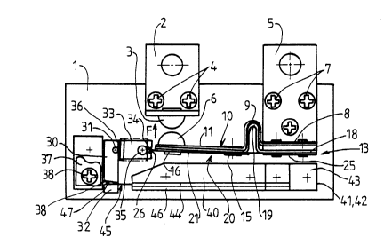
Figure 1 shows a first variant of the invention
implementing a metal wire 41 having shape memory. It is
recalled that a metal having shape memory is suitable for
changing state when raised to a temperature above a given
temperature. In its final state, the material has
dimensions smaller than those it had in the initial
state, and in particular, for a metal wire, that
corresponds to linear contraction.
The device shown in Figure 1 has a baseplate 1 on
which support plates 2 and 5 are fixed by means of
respective screws 4 and 7. The support plate 2 has a
fixed contact 3 in the form of a hemisphere and the
support plate 5 carries a moving blade 10 with a contact
region 6 that is likewise in the form of a hemisphere in
this case, and that is disposed facing the contact region
3. More particularly, the moving contact has two
superposed resilient blades respectively 10 and 20 which
are secured to an extension of the support plate 5 at
respective ends 8 and 18 thereof. Each of the blades 10
and 20 also has a respective region 9 and 19 bent into a
U-shape. Electrical contact between the contact region 6
218~1~7
11
and the contact-making region situated on the support
plate 5 is provided by copper strips, e.g. twelve copper
strips that are 0.1 mm wide and that form a flexible
current path between the contact region 6 and the
contact-making region. The function of the U-shaped
regions 9 and 19 is to enable the blades 10 and 20 to
move without exerting tension on the copper strips 25.
A support plate 40 of elongate shape, disposed in
this case beside the flexible blades 10 and 20 and
running parallel thereto, has two contact regions 41 and
42 at its rear end 43 for conveying a current that heats
the ends of a wire 45 which, in side view, is generally
U-shaped with its branches 44 being received in a guide
46. The central region of the wire forming the bar of
the U-shape and referenced 47 is folded around a semi-
annular groove 38 disposed at one end 32 of an arm of a
rocker 30 pivoted about an axis 31 perpendicular to the
plane of the baseplate 1. The rocker 30 is generally
L-shaped. The branch 33 of the L-shape has an opening 35
towards its end which communicates with the end of the
branch via a slot 34 receiving an extension 36 situated
at the moving ends of the moving blades 10 and 20, and
secured in this case to the flexible blade 20.
Finally, a support plate 37 mounted on the baseplate
1 by a screw 38 serves as an abutment against rotation of
the rocker 30 pivoted about its axis 31.
The device described above has two stable states.
So long as the shape-memory wire 45 has not been heated
by application of a voltage or a current to its ends 41
and 42, the device remains in the configuration shown in
Figure 1. In the event of a battery cell failing, the
bypass current is applied to the shape-memory wire 45.
For example, the wire 45 is connected in series with the
bypass diode whose forward direction corresponds to the
discharge direction of the cell. Thus, in the event of a
cell failing, the wire 45 is heated and it exceeds the
transition temperature for switching to the second state
2182141
12
in which it is shorter in length, thereby causing the
rocker 30 to rotate counterclockwise, having the effect
of causing the moving contact constituted by the blades
10 and 20 to move in the direction of arrow F, it being
given that it is driven by its end 26 engaged in the slot
34 of the branch 33 of the rocker 30. In addition, a
bearing force between the contacts 3 and 6 delivered by a
spring 36 whose end bears against the extension 26 tends
to press the moving blades 10 and 20 and thus the contact
6 against the contact 3 in the direction of arrow F. In
contrast, in the position shown in Figure 1, the force
provided by the spring 36 is situated practically on the
axis of the moving contact 10, 20.
In the first state as shown in Figure 1, the spring
36 bears against the end of the moving blade 10
(extension 26) with a force of about 2 N, for example,
thus ensuring that the blade 10 does not move under the
action of vibration or of acceleration.
When the device is actuated, the rocker 30 rotates
towards the second state. As soon as it goes past its
central, equilibrium position, the spring 36 forces the
assembly comprising the rocker 30 and the blade 10
towards the active position in which the contact 6, 34 is
closed.
Figure 2 shows a second variant of the invention.
The switch comprises a first sleeve 50 generally made of
conductive material which has a cylindrical region 51 at
its rear portion provided with a blind contact opening 49
and having a front portion constituted by a hollow
cylinder 52 comprising, in succession, a wax plug 54, an
optional resilient gasket 55, a plug 59 of an extrudable
material such as indium, an electrically conductive part
60 whose outside diameter is nominally equal to the
inside diameter of the part 52 and having a sealing
gasket 61, the part 60 having a generally cylindrical
central opening 62, and finally an electrically
insulating cylindrical sleeve 80 engaged in the end of
21821~1
13
the cylindrical region 52 and coming into abutment at 81
thereagainst and at 87 against the cylindrical part 60.
The rear cylindrical portion 71 of the contact 70
has a blind contact opening 79 with a central collar 72
in abutment at 84 against the non-conductive cylindrical
part 80, and a front portion constituted by a cylindrical
finger 73 received in the cylindrical central opening 62
and including a frustoconical extension 74 terminating in
a conical end 75.
The two contacts are short-circuited by heating the
wax plug 54 which has a large coefficient of thermal
expansion and which moves the plug of extrudable material
59 towards the end finger 73. Extrusion takes place
through the central opening 62 of the cylindrical part 60
which is advantageously conically flared at 63 towards
the indium plug 59. In addition, an annular reservoir 86
surrounding the root of the finger 73 serves to provide
an additional expansion volume for the indium plug 59.
When the wax 54 is subjected to a rise in temperature,
which may be provided, for example, by the heat given off
by one or more diodes bypassing the battery cell, it
causes the resilient gasket 55 to move and the indium to
be extruded through the frustoconical portion 63 which
forms a front short circuit with the end 75 of the finger
73, which displacement may optionally continue so that
the indium 59 penetrates into the space 62 which tapers
progressively towards the root of the finger 73 and
finally opening out into the expansion cavity 86. The
configuration described provides a large contact area
that encourages low contact resistance, thus encouraging
the passage of high currents of the kind encountered in
the intended application.
The wax used is preferably the expansion wax sold
under the name WESTOWAX DW 91/846 by HULS AG, D-45764
MARL (Germany).
It should be observed that, in section, the
resilient gasket 55 is chevron-shaped, having two
2 1 8~ 1 4 1
_
14
frustoconical regions 57 and 58 directed towards the
finger 73.
Figure 3 shows a third embodiment of the invention
in which the two electrodes 100 and 110 are disposed face
to face in a sleeve 90. The electrode 100 has a contact-
making region 101 and the electrode 110 has a contact-
making region 111. The electrode 100 has a cylindrical
region 102, an annular groove region 103 and a front
cylindrical region 104 which comes into abutment against
an insulating separator washer 108 separating the front
cylindrical portion 104 of the electrode 100 from the
front cylindrical portion 115 of the electrode 110. The
cylindrical region 115 has a plane front face 118
surrounded by an annular opening 117. A low melting
temperature alloy 120, e.g. an indium-tin eutectic alloy,
is housed in the annular space 117 and also covers the
front face 118 at 121, forming a plane face 130. It will
be observed that the portion 122 of the alloy which is
disposed in the annular space 117 is surrounded by a
material that is not wettable by the alloy 120, e.g. a
ring 116 of polytetrafluoroethylene (PTFE).
The space available between the front face 107, the
cylindrical portion 104, and the front face 130 of the
alloy 120 is selected in such a manner that the height h
25 available between the faces 118 and 107 is less than the
height of the dome of liquid that would tend to be formed
in an empty space by the metal mass 120 that is housed in
the annular space 117 and on the face 118. Thus, when
the mass 120 is heated above its melting point, the
liquid dome which tends to form under capillary forces
produces a high-quality short-circuit between the front
ends 104 and 114, and thus between the two contacts to be
short-circuited, i.e. a contact having low resistance and
capable of carrying a high current, of the kind
encountered in the intended application.
The variants of the invention shown in Figures 2 and
3 require an external source of heat. For faults that
2 1 82 1 4 1
_ 1 15
occur during battery discharging, it is possible to use
the heat generated in a temporary bypass diode. If the
fault to be compensated is liable to occur during battery
charging, or if the temporary bypass diode is not
included in the system, it is possible to use a heating
resistance disposed in parallel with the battery cell
under consideration. In the Figure 2 case, the
resistance may be disposed inside the mass of wax 54.