Note: Descriptions are shown in the official language in which they were submitted.
2 ~ 82248
.... .
TITLE OF THE INVENTION
FREQUENCY SYNTHESIZER
BACKGROUND OF THE INVENTION
Field of the Invention
The present invention relates to a frequency synthesizer to be used in a local oscillator
of radio communications equipment.
Description of the Prior Art
In radio communications equipment for mobile telephones or the like, to tr~n~mi.csion
and reception requires switch many frequency channels quickly. To achieve this, a
frequency synthesizer is indispensable to change the frequency of a local oscillator of
radio communications equipment at a high-speed.
Heretofore various methods have been proposed to speed up the switching of frequencies
in frequency synthesizers. Japanese Patent Laid-Open Publication No. Hei 5-503~27
discloses a method in which data for phase error compensation is produced from adifference between an addition result of an integrator in a final stage among integrators
included in a frequency dividing ratio generating means and an addition result of an
integrator of the previous stage thereof, and this data is converted in a D/A converter to
perform phase error compensation.
Furthermore, FIG. 11 shows a frequency synthesizer of fractional divider type
described by Adachi, Kosugi, Ueno, and Nakabe in "High-Speed Frequency SwitchingSynthesizer Using a Fractional Divider Method" in Electronic Communication
Information Journal C-l, vol. J76-C-I, No. 11, pp445-452. In the frequency synthesizer
shown in FIG. 11, the reference frequency signal of a crystal oscillator 1 is divided in a
fixed frequency divider 2, and is then input to a phase comparator 3. Furthermore, in
FIG. 11, the numerals respectively designate: 4, a charge pump for converting and
outputting an output of phase comparator 3 into a current or voltage; 5, a loop filter for
filtering the signal output of charge pump 4; and 6, a voltage-controlled oscillator (VCO)
21 82248
in which an oscillation frequency is controlled by an output of loop filter 5. An output
of voltage-controlled oscillator 6 is fed back to phase comparator 3 through a variable
frequency dlvider 7. A frequency dividing ratio generating means 8 is shown indetail in
FIG. 12, and comprises an adder 10, and an integrator 100 consisting of an adder 11 and
a latch 15. Adder 11 has a carry-out signal CO which is output when the addition result
is 2M or higher. This output and a preset frequency dividing ratio value N of variable
frequency divider 7 are added at adder 10, and the addition result is input to variable
frequency divider 7. A clock for latch 15 is supplied from fixed frequency divider 2.
The operation of frequency dividing ratio generating means 8 of the above-
mentioned prior art is described hereinafter. N is the integral part of the frequency
dividing ratio to be set and A is the decimal part so that the frequency dividing ratio to
be set can be expressed as N+~. In the above-mentioned conventional example, an
increment step of the decimal part ~ is l/2M and
~ = m/2M
for an arbitrary preset value m, where m is an integer in the range O<m<2M. Adder 11
adds m to the output of latch 15, and, when the addition result reaches 2M and causes an
overflow, outputs carry-out signal CO. When an integer m is fed to an input of
integrator 100 comprising adder 11 and latch 15, an overflow occurs at a rate of once
every 2M/m clocks, and the carry-out signal CO is output. This is set to 1 and added to
frequency dividing ratio N at adder 10 to produce a frequency dividing ratio for variable
frequency divider 7. As a result, the frequency dividing ratio is N for 2M/m-l times out
of 2M/m clocks, and N+l for the remaining 1 time. Therefore, the average frequency
dividing ratio becomes N+m/2~ and the desired frequency dividing ratio can be obtained
by appropriately setting m.
FIG. 13 is a waveform diagram showing an operation when M=2 and m=l. In this
case, a preset value m=l and the output of latch 15 are fed to the input terminals of
adder 11, which is a 2-bit adder. The addition result of adder 11 increments by 1 each
2 1 82248
time a clock is supplied, as shown in FIG. 13 (b), and when this value reaches 4, adder
11 outputs a carry-out signal CO, as shown in (c) of the same figure, and the addition
result of adder 11 becomes 0. The addition of the carry-out signal CO and the
frequency dividing ratio N at adder 10 is output as shown in (d) of the same figure.
The phase error in the case of the above-mentioned composition becomes a steppedconfiguration as shown in FIG. 13 (e). This occurs since the frequency dividing ratio,
which should by design always N+1/4, is appropriately changed to N and N+l, and has
a period of 2M times the clock period, the amplitude of which takes on a value of the
integration value of the frequency dividing ratio error multiplied by 2~ (rad). The phase
error is converted into a voltage or current at phase comparator 3 and charge pump 4,
then enters VCO 6 through loop filter 5, and an output of VCO 6 is modulated so that
spurious emissions are generated at an interval of l/2M times the reference frequency fref.
FIG. 14 shows a z transform of frequency dividing ratio generating means 8 shownin FIG. 12. In this conventional example, integrator 100 results in multiplying 1/2M by
integer m and performing integration, so that a value A which is input by an adder 34 in
the z transform of frequency dividing ratio generating means 8 is ~ = m/2M. Adder 11 of
frequency dividing ratio generating means 8 shown in FIG. 12 outputs the carry-out
signal each time an overflow occurs, and the output of adder 11 takes on a value for the
present integration value from which 2M is subtracted, so that frequency dividing ratio
generating means 8 in the z transform, as shown in FIG. 14, comprises a l-clock delay
circuit 35 in the z transform, an adder 36 in the z transform, and a quantizer 37 in the z
transform. Therefore, the decimal part ~' which is output from frequency dividing ratio
generating means 8 of FIG. 14 is expressed in formula (1) below.
+QI(l-Z-I) (1)
Here, Q,(l-Z-~) corresponds to an error of the frequency dividing ratio, and phase
2 1 82~48
error Q, becomes the time integral. As can be seen from FIG. 14, phase error Q,
becomes the output of adder l l with inverted polarity and divided by 2M
In a fractional divider method having the above-mentioned composition, it is
necessary to narrow the loop band to suppress the spurious emissions. As a result, it is
difficult to speed up the switching of frequencies in frequency synthesizers.
The above-mentioned prior art also describes a frequency synthesizer of fractional
divider type which solves these types of difficulties found in the conventional example.
FIG. 15 shows frequency dividing ratio generating means 8 having the same composition
as the one described in the prior art. Although frequency dividing ratio generating
means 8 in this case is similar to those in the above-mentioned conventional example in
having integrator 100 con~i~ting of adder lO, adder 11, and latch 15, it further includes
an integrator 101 consisting of an adder 12 and a latch 16, and a differentiator 102
consisting of an adder 13 and a latch 17, where an output of differentiator 102 is input
to adder 10. The output of adder 11 is fed into adder 12 and integration is performed,
and its carry-out signal CO is time differentiated at differentiator 102, then added with
the carry-out signal CO of adder 11 at adder 10. The clock for latches 15, 16, and 17 is
supplied from fixed frequency divider 2.
A result of the z transform on above-mentioned frequency dividing ratio generating
means 8 is shown in FIG. 16 and comprises adder 34 in the z transform, 1-clock delay
circuit 35 in the z transform, adder 36 in the z transform, and quantizer 37 in the z
transform. Although this is similar to FIG. 14, adders 38, 39, 41, and 43 in the z
transform, 1-clock delay circuits 40 and 44 in the z transform, and quantizer 42 in the z
transform are further included. From this figure, an output X, of quantizer 37 and an
output X2 of adder 43 are respectively
Xl= ~-Z-~Ql+ Ql = ~+(l-Z l)Ql (2)
X2 = (l-Z-~)(-Q~-Z-IQ2+Q2) 2 1 8 2 2 4 8
= -(l-Z l)Ql+(l-Z l)2Q2 (3)
Xl+X2= ~ +(l-Z~l)2Q2 (4)
As can be seen from the formulas above, by composing frequency dividing ratio
generating means 8 as shown in FIG. 16, the error of the frequency dividing ratio
becomes Q2(1-Z l)2 so that the phase error becomes its integration value Q2(1-Z-').
Compared to the above-mentioned conventional example, since Ql is canceled and atime differentiation is performed on Q2, the frequency characteristics of the phase error
are shifted toward the high band. Thus, since the PLL having low-frequency bandpass
characteristics allows spurious emissions to be easily removed, the loop band can be set
wider than in the above-mentioned conventional example, enabling high-speed frequency
switching.
Output waveforms showing an operation in each compositional element of
frequency dividing ratio generating means 8 are shown in FIG. 17 where the carry-out
signal CO of adder 12 is FIG. 17 (e), the output of adder 13 is (f) of the same figure,
the output of adder 10 is (g) of the same figure, and the phase error is (h) in the same
figure. The frequency characteristics are shifted toward the high band so that low-
frequency spurious emissions can be suppressed.
Although a case in the above-mentioned conventional example was described
where integ~ors were connected in cascade in 2 stages, if integrators are connected to n
stages, as shown in FIG. 18, with the carry-out signal CO of an integrator 106 of the nth
stage differentiated to the (n-1)th order, and the sum of the differential values for all
stages is taken, the z transform of decimal part ~' of the frequency dividing ratio
becomes
2 1 82248
,+(l-Z 1)nQn (5)
and a phase error ~3E becomes
~E = 27~(1-Z-I)n-~Q (6)
Therefore, spurious emissions at the low band can be further suppressed.
However, to sufficiently reduce the spurious emissions using the prior art
mentioned above, it is necessary to set the reference frequency fref, which is the output
signal of the frequency divider, to an extremely high value; in order to do this, it is
necessary to have a phase comparator which is capable of phase comparison operations
at a high frequency. Therefore, use of a phase comparator employed in conventional
PLL-ICs and fabricated from a process such as CMOS having slow operations presented
a difficulty, and low power consumption and low cost were difficult to achieve.
SU~ARY OF THE INVENTION
It is therefore an object of this invention to solve the above-mentioned problems and to
provide a low power consumption, low cost, frequency synthesizer of fractional divider
type which is capable of sufficiently reducing spurious emissions at a phase comparison
frequency lower than that of frequency synthesizers of fractional divider type in
conventional examples.
The frequency synthesizer in accordance with this invention includes a crystal oscillator,
a fixed frequency divider which divides the output of the crystal oscillator to output a
reference frequency, a voltage-controlled oscillator, a variable frequency divider which
divides the output of the voltage-controlled oscillator at a frequency dividing ratio
provided by a frequency dividing ratio generating means, a phase comparator which
detects and outputs a phase difference of the reference frequency and an output of the
? 1 82248
variable frequency divider, a loop filter which smoothes the phase difference signal
output from the phase comparator to output a signal which controls the above-mentioned
voltage-controlled oscillator, and the frequency dividing ratio generating means which
provides and controls an integer frequency dividing ratio to the above-mentionedvariable frequency divider.
A phase synchronization loop is composed to control the voltage-controlled oscillator
with the output of the above-mentioned loop filter, and the above-mentioned frequency
dividing ratio generating means, comprising n stages (n=1,2,3,...) of integrators connected
in cascade and n-1 differentiators for differentiating carry-out signals of the integrators,
are composed so that a phase error generated at the above-mentioned variable frequency
divider is obtained from an output of the adder included in the integrator in a final stage
of the frequency dividing ratio generating means and a phase error compensation value
is output.
The frequency synthesizer further includes a phase error compensating means for varying
the pulse width of a signal to be used for comp~n~ting for phase error based on the
phase error compensation value which is output from the above-mentioned frequency
dividing ratio generating means.
Furthermore, the frequency dividing ratio generating means comprises integrators,
differentiators, and one adder, where the integrators are connected in cascade to n stages
and the carry-out signal of the integrator in the ith stage is differentiated to the (i-l)th
order.
The outputs of the differentiators are all input to the adder where a sum is taken with the
integral part of the frequency dividing ratio, and the result is input as the frequency
dividing ratio of the variable frequency divider.
Furthermore, by differentiating to the (n-l)th order the integration result of the integrator
of the nth stage, the phase error compensation value is extracted and input to the phase
error compensating means.
2 1 82248
In the phase error compensating means, the pulse width of the signal to be used for
compencating for phase error is varied to compensate for the phase error by switching
between operation or non-operation of a current supply or voltage supply in accordance
with a value counted by the fixed frequency divider.
Furthermore, the phase error compensating means comprises an adder for adding a phase
error compensation value extracted from the frequency dividing ratio generation circuit
with a preset value and for outputting the result; a subtracter for subtracting the phase
error cornpensation value extracted from the frequency dividing ratio generation circuit
from a preset value and for outputting the result; and a plurality of comparators for
performing comparisons on outputs of the adder and subtracter and the value counted by
the fixed frequency divider so that the pulse width of a signal to be used for
compensating for phase error is varied to compensate for the phase error by passing
outputs of the comparators through gates and flip-flops and outputting a control signal
for switching between operation and non-operation of the current supply or voltage
supply.
The outputs of the phase comparator and phase error compen~ting means are
handled as current outputs, and the phase comparator and phase error compen~tingmeans are directly connected. The loop filter includes a frequency trap which adapts to
a predetermined frequency.
An output of a reference frequency divider is delayed by one period of the signal
output by the crystal oscillator. Furthermore, a comparator for comparing the value
counted by the reference frequency divider with a predetermined value, and a flip-flop
for inputting the output of the comparator while using the crystal oscillator output as a
clock are included, where the output of the flip-flop is used as a clock for the integrators
and differentiators of the frequency dividing ratio generating means.
The frequency dividing ratio generating means in this invention is capable of
varying m time the frequency dividing ratio to be provided to the variable frequency
21 82248
.._
divider, and providing a specific decimal frequency dividing ratio as an averagefrequency dividing ratio to the variable frequency divider. The variable frequency
divider divides the oscillation signal from the voltage-controlled oscillator (VCO) in
accordance with the frequency dividing ratio generated by frequency dividing ratio
generating means and outputs the result to the phase comparator. The phase comparator
compares the reference frequency output by the fixed frequency with the phase of the
signal output by the variable frequency divider and controls the charge pump in
accordance with the phase difference. The charge pump performs charging and
discharging of the loop filter in accordance with the output of the phase comparator, and
performs control of the VCO. The phase error comp~ncating means control the pulse
width of the signal to be used for compencating for phase error based on the phase error
compensation value which is output from the frequency dividing ratio generating means,
and compensates for the phase error caused by changes in the frequency dividing ratio of
the variable frequency divider.
The frequency dividing ratio generating means comprise n (1,2,3,...) integrators, n-l
differentiators, and multiple adders, so that the frequency characteristics of the phase
error are shifted toward the high band. Since the PLL having low-frequency bandpass
characteristics easily enables spurious emissions to be removed, the loop band can be set
even wider to enable high-speed frequency switching. It is not necessary to set reference
frequency frCf~ the output signal of the frequency divider, particularly high, and spurious
emissions can be sufficiently reduced at a phase comparison frequency even lower than
that in the conventional example, resulting in a low power consumption and low cost
frequency divider of fractional diver type.
BRIEF DESCRIPTION OF THE DRAWINGS
FIG. 1 is a block diagram showing an embodiment of a frequency synthesizer
according to this invention.
2 1 82248
FIG. 2 is a circuit diagram showing a frequency dividing ratio generating means to
be used in the embodiment shown in FIG. 1.
FIG. 3 is a circuit diagram showing an embodiment of a phase error comp~nc~ting
means to be used in the embodiment shown in FIG. 1.
FIG. 4 shows a fixed *equency divider in the embodiment shown in FIG. 1.
FIG. 5 shows a clock generating means in the embodiment shown in FIG. 1.
FIG. 6 shows a waveform of a phase error that is output to the phase comparator
of the embodiment shown in FIG. 1, and an output waveform of the phase error
compenC~ting means.
FIG. 7 is a waveform diagram showing an operation to the phase error
compen~ting means shown in FIG. 3.
FIG. 8 is a circuit diagram showing a second embodiment of a frequency dividing
ratio generating means to be used in this invention.
FIG. 9 shows frequency characteristics of a loop filter of a third embodiment to be
used in this invention.
FIG. 10 shows an operation of a fourth embodiment of this invention.
FIG. 11 is a block diagram showing a conventional synthesizer.
FIG. 12 is a circuit diagram showing one example of a conventional frequency
dividing ratio generating means.
FIG. 13 is a waveform diagram showing an operation of a conventional frequency
dividing ratio generating means.
FIG. 14 shows a z transform of the frequency dividing ratio generating means
shown in FIG. 12.
FIG. 15 is a circuit diagram showing another example of a conventional frequencydividing ratio generating means.
FIG. 16 shows a z transform of the frequency dividing ratio generating means
shown in FIG. 15.
21 8~-248
FIG. 17 is a waveform diagram showing an operation of the frequency dividing
ratio generating means shown in FIG. 15.
FIG. 18 is a circuit diagram showing another example of a conventional frequencydividing ratio generating means.
DETAILED DESCRIPTION OF THE PREFERRED EMBODIMENTS
First Embodiment
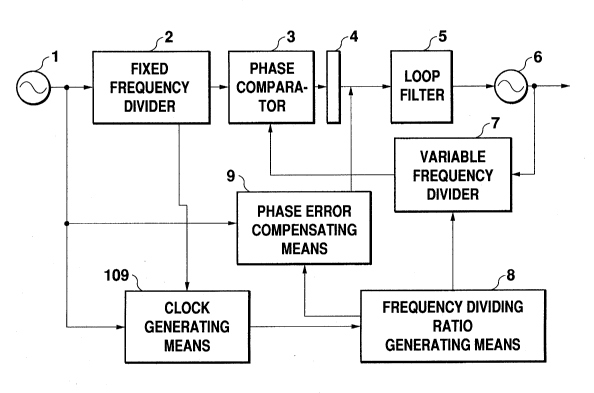
The following describes a first embodiment of this invention. FIG. 1 is a block
diagram showing a f1rst embodiment of this invention wherein the numerals designate
respectively: 1, a crystal oscillator; 2, a fixed frequency divider for dividing the output
of crystal oscillator 1 and providing a reference frequency fref to a phase comparator 3; 4,
a charge pump; 5, a loop filter; 6, a voltage-controlled oscillator; 7, a variable frequency
divider for performing frequency division on the output of voltage-controlled oscillator 6
in accordance with a frequency dividing ratio. This composition is the same as that of
the conventional example shown in FIG. 11. Further, in FIG. 1, numeral 8 designates a
frequency dividing ratio generahng means. Numeral 9 designates a phase error
compenC~ting means and, in this embodiment, the output of phase error compen~ting
means 9 is joined with the output of charge pump 4. Numeral 109 designates a clock
generating means for providing a clock to the frequency dividing ratio generating means.
As shown in FIG. 2, frequency dividing ratio generating means 8 of this
embodiment comprises an integrator 100 consisting of an adder 11 and a latch 15, an
integrator 101 consisting of an adder 12 and a latch 16, a differentiator 102 consisting of
an adder 13 and a latch 17, a differentiator 103 consisting of an adder 14 and a latch 18,
and an adder 10 which adds the outputs of integrator 100 and differentiator 102 with a
frequency dividing ratio N and outputs the result to variable frequency divider 7. The
differences with the conventional example shown in FIG. 12 are the new addition of
integrator 103 consisting of adder 14 and latch 18, and the connections of the output of
21 82248
adder 12 to the inputs of adder 14 and latch 18 of differentiator 103.
The operation of above-mentioned frequency dividing ratio generating means 8 is
described hereinafter.
The operations of integrator 100, integrator 101, differentiator 102, and adder 10
are the same as in the above-mentioned conventional example, and the output frequency
dividing ratio is also the same. Further, phase comparator 3 to be used in this
embodiment connects a current output type charge pump 4, and the current value of its
current supply is ID (A). From FIG. 16, phase error ~E, which is output from frequency
dividing ratio generating means 8, is
~ 3E = 27~(1-Z )Q2 (7)
As can be seen from the figure showing the z transform shown in FIG. 16, Q2 is the
inverted polarity of the output of adder 12 included in integrator 101, and multiplied by
2M. In this embodiment, since the output of adder 12, after being dirrerelltiated by
differentiator 103, is to be used as phase error compensation value Ee~ the output of
adder 12 is input to differentiator 103, and the output of differentiator 103 is input to
phase error compensating means 9, to perform compensation for the phase error. If the
actual phase error is /~3E~ the value of phase error compensation value Ee becomes
E~=- 2 ~3E (8)
An example of a composition of a phase error compensating means 9 is hereinafterdescribed based on FIG. 3.
A compositional example of phase error compensating means 9 in this embodiment
is shown in FIG. 3. Phase error compensating means 9 comprises a comparator 19, a
12
- ` 2 1 ~2248
comparator 20, a comparator 21, a comparator 22, an OR circuit 23, an OR circuit 24,
an AND gate 25, an AND gate 26, a current supply 28, a current supply 29, an inverter
27, an adder 30, an adder 31, an adder 32, an adder 33, a flip-flop 45, and a flip-flop 46.
Phase comparator 3 in this embodiment performs phase comparison at a trailing edge,
and charge pump 4 is of a current output type. Further, current supply 28 and current
supply 29 can switch between an operating state and a non-operating state according to
control signals provided from AND gate 25 and AND gate 26. If fout is the frequency of
the output signal of VCO 6 and frequency fTcxo is the frequency of the output signal of
crystal oscillator 1 which is input to fixed frequency divider 2, a current value Ic of
current supply 28 and current supply 29 is determined from formula (9).
ID = 2IC
fo~2 fr~xo
(9)
Among the signals which are input to this phase compçn~hng means 9, LOAD is
a value which again performs loading after the up counter in fixed frequency divider 2
outputs the ripple carry as a frequency divider output. The counter contents represent a
value counted by the up counter in fixed frequency divider 2, and comparisons are
performed on a terminal B with the value at a terminal A of comparator 19, comparator
20, comparator 21, and comparator 22. Comparator 19 and comparator 21 output a high
level signal if the counted value at terminal A is larger than the value at terminal B, and
comparator 20 and comparator 22 output a high level signal if the counted value at
terminal A is smaller than the value at terminal B. Values created from adder 30, adder
31, adder 32, and adder 33 are input at terminals B, where a value 2n-l-E~3 which is
output from adder 30, a value LOAD+E~ which is output from adder 31, a value 2n-1-E~
which is output from adder 32, and a value LOAD-E,3 which is output from adder 33, are
fed to terminals B of comparator 19, comparator 20, comparator 21, and comparator 22,
13
21822`48`
respectively. The value E~3 given here is a compensation value for the phase error in a
two's complement represe~ lion. Further, E~ (MSB) represents the most significant bit
of E~.
FIG. 4 shows a compositional example of fixed frequency divider 2 in this
embodiment. A block 110, a traditional n-bit up counter, is composed so that the LOAD
value, which is set in advance each time the ripple carry is output, is read and the up
counter restarts. The frequency dividing ratio of fixed frequency divider 2, which is
outputting the ripple carry, is 2n-LOAD. A block 111 is a flip-flop which re-times and
delays by one period the ripple carry of the up counter to synchronize the phase with the
compensation signal.
FIG. 5 shows a compositional example of clock generating means 109 which
generates the clock for frequency dividing ratio generating means 8 in this embodiment.
A block 112 is a comparator which compares a preset value 2n-9 with the value counted
by up counter 110, which is included in fixed frequency divider 2, and outputs a high
level signal only when they are equal, and a block 113 is a flip-flop which re-times the
output of comparator 112 while using the output of the crystal oscillator as a clock.
An operation of this embodiment is described hereinafter with reference to FIG. 6
and FIG. 7. In FIG. 6, (a) and (c) respectively show the waveforms caused by phase
error which are output by charge pump 4 when E~3=3 and Eg=-2, and (b) and (d)
respectively show the waveforms of the phase error compensation signals which are
output by phase error compen~ting means 9 to compensate these waveforms.
FIG. 7 is a waveform diagram showing operations of various parts. As a typical
example, a case where E~=3 is described here. In FIG. 7, the alphabetic characters
designate respectively: (a), output of flip-flop 113 included in clock generating means
109; (b), output of comparator 112 included in clock generating means 109; (c), phase
error compensation value provided to phase error compensating means 9; (d), contents of
the up counter included in fixed frequency divider 2; (e), ripple carry of the up counter
21 82248
included in fixed frequency divider 2; (f), output of flip-flop 111 included in fixed
frequency divider 2; (g), output of comparator 19 included in phase error compensating
means 9; (h), output of comparator 20 included in phase error compensating means 9;
(i), output of OR circuit 23 included in phase error compensating means 9; (j), output of
OR circuit 24 included in phase error compensating means 9; (k), output of AND gate
25 included in phase error compen~tin~ means 9; (1), output of AND gate 26 included
in phase error compenc~ting means 9; (m), output of flip-flop 45 included in phase error
compçn~ting means 9; (n), output of flip-flop 46 included in phase error compensating
means 9; (o), MSB of E!3
An explanation is given here with the contents of up counter 110. When the
counter conte~ of up counter 110 reach 2n-9, comparator 112 outputs a high levelsignal. When the contents of up counter 110 are 2n-8, flip-flop 113 performs re-timing
of the comparator output and outputs a high level signal which is used as a clock at
frequency dividing ratio generating means 8 where integration is performed, and a new
phase error compensation value E~=3is output. When the counter contents of up counter
110 become 2n-3~ comparator 19 outputs a high level signal and the output of OR circuit
23 goes high level. Since E~is a two's complement representation and the MSB of E~is
low when E~=3, AND gate 25 passes along the output of OR circuit 23. When the
counter conte,ll~ of up counter 110 are 2n-2, flip-flop 45 re-times and outputs the output
of AND gate 25 to current supply 28 to control the operating state. When the counter
conte~ of up counter 110 become 2n-1, up counter 110 outputs a ripple carry and
performs reading of LOAD. When the counter contents of up counter 110 are LOAD,
flip-flop 111 re-times and outputs the ripple carry-out of up counter 110 for use as the
output signal of fixed frequency divider 2. When the counter contents of up counter 110
become LOAD~ the output of comparator 19 goes low level. However, the output of
comparator 20 goes high level so that the output of OR circuit 23 remains high level.
When the counter contents become LOAD+3, comparator 20 outputs a low level signal,
2182248
.
the output of the OR gate goes low level, and the output of the AND gate goes low
level. When the counter contents of up counter 110 are LOAD+4, the output of ANDgate 25 is re-timed by flip-flop 45 to control current supply 28 to the non-operating
state. Through these operations, the pulse width becomes equal to 6 periods of crystal
oscillator 1, and the value of the time integral of the current supplied by current supply
28 is expressed as follows:
--3 =--3
frcxo fo~t2M
(10)
where the phase error ~E of fout generated from variable frequency divider 7 at this time
becomes
=-- 3 2~
2 (11)
The waveform generated in phase comparator 3 from phase error ~E iS the wareform of
(a) in FIG. 4 and the integration value of the current of this waveform is expressed in
formula (12) below.
_ 3 . ID
2M f (12)
Thls value becomes equal to the integration value of the current output from phase
error compensating means 9 expressed in formula (10). Furthermore, since the pulse
2 1` 82248
generated from phase error is generated near the trailing edge of the output of fixed
frequency divider 2, the phase error compensation signal and the phase of the pulse
generated from phase error can be synchronized by re-timing the output of up counter
110 at flip-flop 111. In this manner, phase error compensating means 9 perform
compensation on the current generated from phase comparator 3 due to phase error ~3E
Second Embodiment
The integrators were connected in two cascaded stages in the above-mentioned
embodiment. FIG. 8 shows an embodiment where the integrators connected in cascade
are further increased in number so that the number of stages is n. In this case, the
deçim~l part ~' of the frequency dividing ratio becomes
~ = ~+(1-Z ) Qn (13)
and the phase error ~E becomes
~E = 2~1(1-Z ) Qn (14)
Q is the output of an adder 104 included in an integrator 106 of the nth stage which is
the final stage, and this output is differentiated to the (n-l)th order at a differentiator
107, then input by phase error compensating means 9 to perform compensation for the
phase error.
In accordance with this embodiment, superior spurious suppression can be achieved
since the outputs of multiple integrator stages are differentiated to obtain the phase error
compensation value.
Third Embodiment
If the suppression of spurious emissions is still insufficient, even though
compensation is performed in this manner, the use of a filter having amplitude-frequency
17
- ` 2 1 82248
_
characteristics shown in FIG. 9 for loop filter 5 is effective. This filter comprises a lag-
lead filter and a frequency trap having extremely shallow characteristics, and can
perform sufficient suppression of spurious emissions if the frequency trap is set to a
frequency equal to the especially problematic detuning frequency when spurious
emissions are generated in the frequency synthesizer output signal.
Fourth Embodiment
This embodiment is composed so that current supply 28 and current supply 29,
included in phase error compensating means 9, output a current of IB+IC when thecontrol signal is high level and a current of IB when the control signal is low level.
FIG. 10 explains an operation of this embodiment when E=3 is input to phase error
compenC~hng means 9. In this figure, (a) is an output of flip-flop 45 which becomes a
control signal, (b) is a timing waveform of current supply 28, (c) is a timing waveform
of the output of current supply 29, and (d) is a timing waveform of the output of phase
error compPnc~hng means 9.
As can be seen from FIG. 10, since the current output of phase error compçnc~ingmeans 9 is the result of subtracting the output of current supply 29 from the output of
current supply 28, the current value of the signal (d) which is output by phase error
compPnc~ting means 9 is the equivalent to that in the first embodiment, and
compensation for the current generated from charge pump 4 due to phase error ~3E can be
performed.
In accordance with the frequency synthesizer of this invention, the spurious
performance can be improved considerably and frequency switching can be performed at
high speeds without using, as in conventional methods an extremely high phase
comparison frequency and even when using a relatively low phase comparison
frequency. Furthermore, an inexpensive, low power consumption, high-speed switching
frequency synthesizer can be realized since phase error compensation can be performed
without using complex analog circuitry such as D/A converters.
18
2 1 82248
While there has been described what are at present considered to be preferred
embodiments of the invention, it will be understood that various modifications may be
made thereto, and it is intended that the appended claims cover all such modifications as
fall within the true spirit and scope of the invention.
19