Note: Descriptions are shown in the official language in which they were submitted.
21g2'~97
W0 96118245 P~ .'0 ~783
PHASE LOCKED LOOP CONTR~)LLED FREQUENCY SYNTHESIZER FOR USE IN
FREQUENCY HOPPING.
Field of the Invention
6 Thi6 invention relates in general to cnmmlmi~tinn~ systems, and
more particularly to a method fol imrl~m~ontin~ frequency hopping in a time
domain system.
gAPk~round to th~ Invention
Base station transceivers for TDMA cnmmllni- ~tinnC systems such as
DCS1800, have to be capable of ~u~uluulLillg frequency hopping on a time slot
by time slot basis. This requirerrlent inflll~ncl~ the linearity of the
transmitter since power ramping must be employed to reduce spurious
emissions from the step changes in transmit frequency. In order to reduce
16 side-lobe levels it is desirable to spread the power ramp over a wide period.
As a result, the synthesiser has an extremely small window in which to hop.
Several problems are ~ uullL~I~d in the imrl~m~nt~inn of such a
synthesiser, such as fast acquisition, low noise and high resistance to
frequency pulling.
Slow frequency hopping is commonly employed in TDMA based
cellular systems. In slow frequency hoppirlg (SFH) the L~u, u~ u~ y channel is
altered at a rate which is lower than the bit rate. For example, in GSM the
frequency channel is switched on a burst by burst basis. In GSM, SFH is
employed for two reasons, to pro~ide frequency diversity for slow moving
26 mobiles and also inteferer divers~ty for increasing system capacity.
In order to support slow L~u,u~ y hopping, it is necessary for the
base station to support all time slots during the TDMA frame, consequently,
the synthesiser has to frequency hop during a short period which eYists
between time slots, which is generally referred to as the guard period. The
frequency hopping m~nh~nicm is usually slncnmrlich~-l by employing two
Phase-Locked Loop frequency sy~thesisers and a single pole double throw
switch. When one synthesiser is providing the transmitting frequency, the
other is l~pl U~ l dlluued and returled to the ne~t. The retuning process has tobe zlr~nmrli~h~d within one time slot so that the required tr~n~mirt;n~
36 frequency is sufficiently stable before being directed to the transmitter
output. This operation is illustrated in FIG. 1, which shows the
tr~nqmitiin~ frequency allocatioIl per time slot and the guard period.
~,~ S2~ 1
wo 96/18245 r~ ,5:c l783
The switching mP~h,lni~m which selects the appropriate synt7~lesiser,
causes an impul7sive mi~m7~trh in load impedance which pulls the
synthesiser off frequency. This causes a corresponding phase disturbance
inside the loop which is eventually corrected by the loop feedback
5 ,.,~,1lt"i~,.. However,ifthesynthesiserisunabletorespondquickly,then
a large phase excursion can occur at the beginning of the time slot resulting
in ci~nifi~nt p~rfnr7n~n~ degradation.
The prior art solution to this problem is to provide an increased
reverse isolation between the switch and the synthesiser. This is achieved
10 by cascading severa7, gain blocks interleaved withlarge .~ltt~nll~t.~rs. There
are several drawbacks with the prior art solution including.
i) The wide band noise p~lru,luallce of the transmitter can ci~nifi(~,lntly
degrade,
15 ii) increasing the number of stages increases the ( nmrtmPnt. count,
iii) the power ~-)n~llmrfir7n of a synthesiser can increase by as much as
40%,
iv) the required synthesiser board area can increase by upto 20%.
It is desirable to have a method that wou,d reduce the complexity and
expense of the present frequency hopping schemes in time domain systems.
S7lmm~rv of th~ Tnvention
According to the present invention, there is provided a method for
imr7,~m~ntin~ frequency hopping in a time domain system having at least a
first synthesiser including the steps of locking onto a first frequency by the
_rst synthesiser in wide loop bandwidth mode, transmitting from the first
synthesiser, and converting to a narrow bandwidth mode on the first
synthesiser after a delayed period of time.
In a preferred ~mho~lim~nt the time domain system is a TDMA
system.
Brief Descri~tion of the Drawin~
FIG. 1 illustrates a TDMA frame structure.
FIG. 2 illustrates power ramping employed du,-ing a guard period of
the TDMA frame structure of FIG. 1.
2182297 :
~ WO 96/18245 r~ 783
FIG. 3 illustrates a f~ow chart for a preferred Pmho~imPnt, of the
present invention.
FIG. 4 is a block diagram of a synthesiser according to the present
invention.
FIG. 5 qimlllAt.inn results of a byl.Llle6l6~l according to the prior art.
FIG. 6 RimlllAtinn results of a synthesiser employing the method of
the present invention.
D~PtAilP-l Descr,intion ofthe Preferred Embo~1imPnt
FIG. 1 shows a frame 2 axld slot 4 structure for a time division
multiple access (TD~IA) system employing frequency hopping. The slots are
shown changing frequency from one slot to the next thus each ~u~,~,e~biv~
TDMA slot 4 is shown as being ~;rAncmittPd on a different frequency.
Frequencies are chAnged during a guard period 6 between two slots. Two
synthesisers may be employed to achieve such rlt,~lut,ll~ hopping.
One synthesiser may be trAncmittin~ while a second synthesiser is
tuning to the next slot's rl~ u~u~"y. The synthesisers then switch during the
guardperiod6. The~yllLllesls~l thatwas ~l..l,~,,.;l';..~powersdownand
stops L~ and the synthesiser that was tllning powers up and starts
trAnqmitt~nF on a new r. t,~lu~u~. Dual loop bandwidth is employed which
has independent control of both noise and switching speed.
In order to suppress the spectral emissions from the rapid switching
of frequency channels, power raxnping is employed during the guard period,
This is illustrated FIG. 2 which shows slot n ramping down 20, 21 and slot
n+1 ramping up 22, 23. The ~lP~i~nAt.Ptl end of the nth time slot 20 is where
the trAnqmittin~ synthesiser begins ramping down and is the beginning of a
guard period 20. At the end of the ramp down 21 and before the beginning
of the ramp up 22 of the tuned tx ansmitter is when the synthPgiePrq switch
from trAnqmittine to tuning and from tuning to trAnRmittin~, The
synthesiser that switches from tuning to trAngmittin~ begins ramping up 22
and ends ramp up near the starl, of the n+1 burst 23, the end of the guard
period.
FIG, 3 shows a method according to the present invention to
implement frequency hopping in a TDMA system as described. While a first
synthesiser S1 is employed as the transmitting frequency as shown in step
38, a second synthesiser S2 is retuned to the next frequency in wide loop
bandwidth mode as in step 30
97
W0 96/18245 r~ .'0 ~783
.
After a finite time pèriod, the second synthesiser S2 locks onto a new
transmit frequency and mslint~ine wide loop bandwidth mode as in step 32.
Referring to FIG. 2 at the end of a slot time 20, the transmitter output
begins to ramp down until it reaches time 21 when the l,ldl~ L~l output
5 power is inhibited as described by step 40 in FIG. 3.
A finite period after ramp down 21 (FIG. 2), the second synthesiser S2
becomes the tr~ncmittin~ r~ u~llcy as in step 34 (FIG. 3) and the first
synthesiser S1 no longer l,I.~ S, step 42. At this point, the second
synthesiser S2 is still in wide loop bandwidth mode.
At the end of the PA inhibit period 22 the transmitter power begins
ramping up. A finite period later, the loop bandwidth converts to narrow
mode operation as in step 36. In step 36, the second s~vnthesiser S2 is in
narrow loop bandwidth mode and the power ramp-up is finished. During the
complete part of the active time slot and the ::lUbS~ ,U~ ramp down period,
the second synthesiser 2 mslints~inc narrow loop bandwidth.
A finite period after the ramp down, the first synthesiser S1 becomes
the tr~ncmittin~ frequency, and the second synthesiser S2 reverts back to
wide loop bandwidth mode for retuning purposes.
This method is repeated and is applied to the first synthesiser Sl.
Thus, a method for imrl~mPntin~ frequency hopping is provided
where a synthesiser locks onto a frequency in wide loop bandwidth mode7
transmits from the first synthesiser, and then converts to a narrow
bandwidth mode after a delayed period of time.
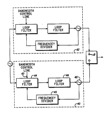
FIG. 4 shows a synthesiser circuit al~ for imrl~m~ni.in~
frequency hopping in a time domain system. The circuit arrangement
permits the imrl~m~nt~tion of the above described method. It consists of
two phase-locked loop synthesisers 40, 42 and a single pole double throw
(SPDT) switch. Each phase-locked loop synthesiser 40 consists of four basic
elements, a phase detector 44, a loop filter 46, a voltage controlled oscillator48 and a frequency divider 45. In order to achieve both narrow and wide
loop bandwidth modes of operation, the gain of the phase detector 44 is
adjusted by means of the bandwidth control line 43 as illustrated in FIG. 4.
The bandwidth control line 43 is a delayed version of the clock which is
employed for selecting the appropriate synthesiser for the tr~ncmit~ing
frequency. When wide loop bandwidth operation is required the bandwidth
control line 43 instructs the phase detector 44 to increase i~s gain
according~y, which results in a corresponding increase in bandwidth. When
229~
~ WO 96/18245 ~ '0 ~783
narrow loop bandwidth operation is required, the bandwidth control ~ine 43
instructs the phase detector 44 to decrease its gain producing a
corrrRrrln-lin,~ decrease in loop ]~andwidt~l.
FIG. 5 shows the cimll17~tirm results of a dual loop bandwidth
5 synthesiser converting to narrow bandwidth before tr~nqmittin~.
FIG. 6 shows the cimlli7~ti~)n results of a dual loop bandwidth
synthesiser . ~ ; . .; . .,g to wide bandwidth mode before tr~n cmitring and
then converting to narrow bandwidth a time after tr~ncmittin,r according to
the method of the present invention. The numbers on FIGS. 5 and 6 relate
10 to the numbers in FIG 2.
The present invention provides an ~JIJdl d1US and method for
imrlem~ntin~ frequency hopping in a time domain system such as a GSM.
The method of the present invention requires a synthesiser to switch to a
narrow loop bandwidth mode afl;er a finite period of time after a channel is
15 hopped.
The benefit of the present invention is twofold. Firstly, due to the
wide loop bandwidth during the guard period rl~4u~7ll~y pulling from
imrefl lnre miqm ltrh~c is reduced. Secondly, no z~l/lition ll circuitry is
required for the provision of high reverse isolation between the SPDT and
20 the VCO
The proposed technique derives the required clock signal from the
burst clock which controls the Sl'DT switch. This signal has to be delayed in
order to provide the loop sufficient time to re-acquire lock-in. However, the
delay has to be short enough to ensure suppression of phase jitter at the
25 start of the burst, since the leng~;h of the loop impulse response will be
increased. Once the loop has converted to a narrow bandwidth its impulse
response remains constant durinlg the active part of the burst and also
during the power ramp down. V~hen the output power is ,cllfliei~ntly small
the power amplifier is inhibited to prevent spurious ~mic~ionc At this point
30 the loop reverts back to its wide bandwidth for hopping to the next frequency,
channel in the next slot. This process is then repeated for the remainder
and successive frames
The present invention combines RF technology with the features of
the time domain system in order to efficiently imrlf~m~nt frequency hopping.