Note: Descriptions are shown in the official language in which they were submitted.
2 1 82334
FIELD OF THE lNV~NllON
This invention relates to the field of
microwave antennas and in particular to a low profile
relatively broadbeam antenna radiator.
BACKGROUND TO THE INVENTION
Low profile antenna radiating elements
generally produce a relatively narrow beam centered at
broadside. This limits the ability of phased arrays of
the radiating elements to scan at low elevation angles.
The microstrip patch antenna formed of plural
conductive layers on a plastic substrate, is a design
which attempts to overcome the above problems. However
this form of element is also very large, and has a
beamwidth which is too narrow for scAnn;ng to low
angles, i.e. close to the horizon.
SUMMARY OF THE I~v~NllON
The present invention is an antenna radiator
which has a small surface area, and thus allows close
element spacing. It has a beamwidth which is adequate
for scAnn;ng small horizontal arrays to the horizon. In
addition, the radiating element is circularly
polarizable and is broadband. The present invention has
a much smaller radiator size than conventional radiating
elements at a given frequency, and has a much broader
beamwidth. It can be used in an array scanned through
larger angles than previous such arrays, without
exciting grating lobes, and while maintaining low
sidelobe levels. Accordingly the element is suitable
for use for mobile satellite communications at L-band
(1525 - 1661 MHz).
In accordance with an embodiment of the
invention, an antenna radiator is comprised of a
rectangular conductive cap disposed over a top of a
dielectric, the cap having an extension over a side of
the dielectric, apparatus for feeding energy to the
2 2 1 82334
radiator adjacent an end of the extension remote from
the cap, and a ground plane spaced from and parallel to
the cap, below the dielectric.
BRIEF INTRODUCTION TO THE DRAWINGS
A better understanding of the invention will be
obtained by considering the detailed description below,
with reference to the following drawings, in which:
Figures 1, 2 and 3 are isometric views of three
embodiments of the invention, respectively,
Figures 4, 5 and 6 are composite plan and side
elevation views of variations of the three embodiments
of the invention,
Figure 7 is an isometric view of plural
radiating elements in an array,
Figure 8 is a plot of an antenna radiation
pattern of a conventional microstrip patch antenna
radiating element, and
Figure 9 is a plot of an antenna radiation
pattern of an embodiment of the present invention.
DETATT~n DESCRIPTION OF EMBODIMENTS OF THE PRESENT
INVENTION
Figures 1, 2 and 3 illustrate the invention as
can be used to provide circular polarization or dual
orthogonal linear polarization. The structure is
comprised of a rectangular conductive cap 1 which is
disposed over a dielectric 3. Extensions 5 from the cap
1 are disposed at the sides of the dielectric 3. The
dielectric is located above a conductive ground plane 7.
The widths of the extensions may be narrower than the
adjacent side widths of the cap 5.
Extending from the cap 1, on sides opposite to
the feed points, are loading elements, preferably
loading stubs (not seen in Figures 1, 2 and 3, but which
will be described with reference to other embodiments).
_ ~ 3 2 1 82334
Circular polarization is achieved by feeding
each of the extensions, preferably via feed pins 9, with
signals which are of equal magnitude but are 90 degrees
out of phase. Linear polarization is achieved by
S feeding the element at only one point, i.e. at only one
of the pins 9, or by feeding both feed pins in phase.
It should be noted that four feed pins can be
used, one on each side. A pair of feed pins on opposite
sides from each other would be excited for each mode of
excitation.
In the embodiment of Figure l, the extensions
5 are at 90 degrees to the plane of the cap l. In the
embodiments of Figures 2 and 3, the extensions 5 are at
less than 90 degrees and more than 90 degrees to the
plane of the cap l, respectively. The embodiments of
Figures 2 and 3 can provide improved axial ratios in
some planes at low elevation angles.
The dielectric can be air, foam, honeycomb or
a solid, such as a polyolefin.
The radiating elements are uniquely small in
size for a given resonant frequency, and which is
particularly useful in the design of phase scanned
arrays. Typical dimensions of the radiator as ratios to
the free space wavelength at the operating frequency,
for an air dielectric, are: length: 0.2; width: 0.2;
height above the ground plane: 0.13. This compares with
a conventional radiating element such as a microstrip
patch radiator, with an air dielectric, in which the
corresponding ratios are: length: 0.45; width: 0.45;
height: 0.07.
It may be seen that with the length and width
of radiators of the present invention being less than
half the corresponding dimension of patch antenna
radiators, less than one quarter the ground plane
surface area is required, allowing more radiators to be
21 8~33~
used in an array for a given space than in a patch
antenna array.
A measured radiation pattern of a prior art
patch antenna radiator on a polyolefin substrate is
shown in Figure 8, and a measured radiation pattern of a
prototype antenna radiator of the present invention
using an air dielectric is shown in Figure 9. Both were
fed signals which provided right hand circular
polarization.
The patch antenna element has a half power
beamwidth of only approximately 63 degrees, while the
half power beamwidth of the present invention is
approximately 94 degrees. It has been determined that
if the present invention had a polyolefin dielectric its
beamwidth would have been even larger than 94 degrees.
Elements can be packed close together,
allowing phased arrays to scan to very large angles off
of boresight without exciting grating lobes and while
maintaining low sidelobe levels.
Turning now to Figure 4, more detailed plan
and elevation views are illustrated of the embodiment of
Figure 1. The loading elements in the form of stubs 11
extend from the conductive cap 1, in the same horizontal
plane as the cap. The pins are soldered to the
extensions 5, and are connected to connectors 13 which
are supported by the ground plane or from a support for
the ground plane.
Preferred dimensions identified by letter for
each part of the radiator are as follows, for a
frequency band of 1525 - 1661 MHz: (a): 18mm; (b): 5 mm;
(c): 38 mm; (d): 3 mm; (e): 3 mm; (f); 12.7 mm and (g):
8 mm. The input impedance of a prototype radiating
element made in accordance with the above dimensions was
about 280 ohms. The feedpoint at the bottom of the
2 1 82334
figure was excited 90 degrees out of phase from the
feedpoint at the side of the figure.
The dielectric can be air, or a solid
dielectric. If the dielectric is air, the structure can
S be supported by the pins 9 and connectors 13. If the
dielectric is solid, the dielectric can provide
structural support. A solid dielectric will reduce the
resonant frequency of the radiating element.
While the dielectric and the cap are described
lo as being rectangular in shape it is intended that
"rectangular" should be construed as meaning either
square or rectangular, square being only special
dimensions of rectangularity.
The conductive ground plane can be a flat
sheet of copper, copper that is plated with tin or gold
or other conductive material. This conductive sheet can
be laminated to fiberglas or some other dielectric
sheet. The ground plane provides a return current path
and also blocks back radiation.
The extensions to the cap, the cap, and the
loading stubs are preferably formed of a continuous
conductive material, which sits over the dielectric (or
dielectric block, if solid). Alternatively, they can be
formed of conductive material deposited and retained on
the surface of the dielectric material.
During operation, currents from all portions
of the conductive material radiate, as do displacement
currents in the dielectric.
It should be noted that the extensions 5 are
important aspects of the design, since they increase the
vertical component of the radiated field relative to
that of conventional elements, particularly at low
elevation angles. They also reduce the input impedance
of the element to a value which can be impedance matched
6 21 82334
. ~
over a broad frequency band. They also provide
connection points to the connector 13.
While each of the extensions 5 perform similar
functions, the use of the two extensions allow circular
S polarization with relative 90 degree phase excitation,
and also allow dual orthogonal linear polarization with
in-phase excitation of both.
The loading stubs provide capacitive loading
on the radiator, reducing the resonant frequency, and
reducing the coupling between the two feed points.
Figure 4 illustrates horizontal loading,
wherein the loading stubs 11 are in the same plane as
the cap 1, and extend over part of, and to the edges of,
the dielectric 3. Figure 5 illustrates vertical
loading, wherein the loading stubs 11 extend along the
sides of the dielectric 3. In this embodiment, the cap
1 covers the top of the dielectric completely. Figure 5
also illustrates that the stubs need not be rectangular
in shape as in Figure 4, but may be L-shaped. Indeed,
any suitable shape of loading stub can be used.
The dimensions of the embodiment of Figure 5
for the frequency given above, are the same as the
embodiment of Figure 4, except for the substitution of
the following dimensions: (h): 18 mm; (i): 15 mm; (j): 6
mm and (k): 5 mm.
Figure 6 illustrates another embodiment of the
invention. In this case, only one extension 5 of the
cap 1 is used, and only one loading stub 11. While
horizontal loading is shown, vertical loading, as shown
in Figure 5 could be used. In this embodiment, the
single connector 13 is excited, resulting in linear
polarization.
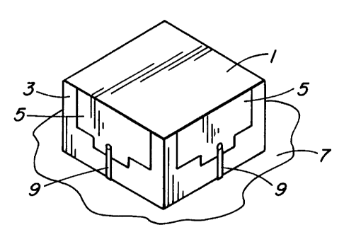
Figure 7 illustrates plural closely packed
radiators, each as any of the radiating elements
described above, fixed above a ground plane 7. The
7 218~3~
array can be scanned in a well known manner, but in
accordance with the present invention, the useful
bandwidth can be relatively broad. The array can scan
to very large angles off the boresight A, as noted
earlier, and as illustrated in Figure 9.
A person understanding this invention may now
conceive of alternative structures and embodiments or
variations of the above. All those which fall within
the scope of the claims appended hereto are considered
to be part of the present invention.