Note: Descriptions are shown in the official language in which they were submitted.
21826 47 CFO 11609 ~
ELECTRON-EMITTING DEVICE AND ELECTRON SOURCE AND
IMAGE-FORMING APPARATUS USING THE SAME AS WELL AS
METHOD OF MANUFACTURING THE SAME
BACKGROUND OF THE INVENTION
Field of the Invention
This invention relates to an electron-emitting
device, an electron source and an image-forming
apparatus comprising such an electron source. It also
relates to a method of manufacturing such an
electron-emitting device, an electron source and an
image-forming apparatus.
Related Backqround Art
There have been known two types of
electron-emitting device; the thermoelectron emission
type and the cold cathode electron emission type. Of
these, the cold cathode emission type refers to devices
including field emission type (hereinafter referred to
as the FE type) devices, metal/insulation layer/metal
type (hereinafter referred to as the MIM type)
electron-emitting devices and surface conduction
electron-emitting devices. Examples of FE type device
include those proposed by W. P. Dyke & W. W. Dolan,
"Field emission", Advance in Electron Physics, 8, 89
(1956) and C. A. Spindt, "PHYSICAL Properties of
thin-film field emission cathodes with molybdenum
cones", J. Appl. Phys., 47, 5284 (1976).
~182647
-- 2 --
Examples of MIM device are disclosed in papers
including C. A. Mead, "The tunnel-emission amplifier",
J. Appl. Phys., 32, 646 (1961).
Examples of surface conduction electron-emitting
device include one proposed by M. I. Elinson, Radio
Eng. Electron Phys., 10 (1965).
A surface conduction electron-emitting device is
realized by utilizing the phenomenon that electrons are
emitted out of a small thin film formed on a substrate
when an electric current is forced to flow in parallel
with the film surface.
While Elinson proposes the use of SnO2 thin film
for a device of this type, the use of Au thin film is
proposed in [G. Dittmer: "Thin Solid Films", 9, 317
(1972)] whereas the use of In203/SnO2 and that of carbon
thin film are discussed respectively in [M. Hartwell
and C. G. Fonstad: "IEEE Trans. ED Conf.", 519 (1975)]
and [H. Araki et al.: "Vacuum", Vol. 26, No. 1, p. 22
(1983)].
A surface conduction electron-emitting device is
typically prepared by arranging a pair of device
electrodes on a substrate, bridging the device
electrode by means of an electroconductive film made of
metal or a metal oxide and then electrically treating
the electroconductive film by subjecting it to a
current conduction process referred to as "energization
forming" in order to produce an electron-emitting
21826~7
-- 3 --
region. In the energization forming process, a
constant DC voltage or a slowly rising DC voltage that
rises typically at a rate of 1 V/min. is applied to the
opposite ends of the electroconductive thin film to
partly destroy, deform or transform the film and
produce an electron-emitting region which is
electrically highly resistive. The electron-emitting
region is part of the electroconductive film where one
or more than one fissures are formed so that electrons
may be emitted therefrom.
Since a surface conduction electron-emitting
device as described above has a particularly simple
structure and can be manufactured in a simple manner, a
large number of such devices can advantageously be
arranged on a large area without difficulty. As a
matter of fact, a number of studies have been made to
fully exploit this advantage of surface conduction
electron-emitting devices. For example, there have
been proposed various types of image forming apparatus
including display apparatus.
Examples of the arrangement of a large number of
surface conduction electron-emitting devices include
electron sources realized by arranging surface
conduction electron-emitting devices to form a number
of parallel rows of devices and connecting the opposite
ends (device electrodes) of the devices of each row to
respective wires (also referred to as common wires) (an
~1826~ l
arrangement often referred to as radder-like
arrangement). (See Japanese Patent Application
Laid-Open Nos. 1-31332, 1-213749 and 2-257552.) As for
display apparatus, there has been proposed a flat panel
display apparatus that is similar to a display
apparatus utilizing liquid crystal but of an emission
type that does not require the use of a back light.
Such a display apparatus can be realized by combining
an electron source comprising a large number of surface
conduction electron-emitting devices and a fluorescent
body that emits visible light when irradiated with
electron beams by the electron source. (See U.S.
Patent No. 5,066,883.)
However, known electron-emitting devices to be
used for electron sources and image-forming apparatus
need to be improved in terms of the efficiency of
electron emission and other electron-emitting
characteristics to provide image-forming apparatus that
can stably produce clear and bright images. The
efficiency of electron emission is described in terms
of the ratio of the electric current running through
the surface conduction electron-émitting device (device
current If) to the electric current generated by
electrons emitted into vacuum from the device (emission
current Ie) when a voltage is applied to the paired
device electrodes and it is preferable that the device
current is held as small as possible whereas the
~1826~7
emission current is made as large as possible. If
stably controllable electron emitting characteristics
and an improved efficiency of electron emission are
achieved for a surface conduction electron-emitting
device, an image-forming apparatus comprising an
image-forming member of a fluorescent body that
produces high quality images at a low power consumption
rate can be realized by using such devices. Such an
image-forming apparatus may be a flat television set
and the drive circuit and other components of such an
image-forming apparatus may be manufactured at low
cost.
Known electron-emitting devices are, however, not
satisfactory in terms of stable electron-emitting
characteristics and electron-emitting efficiency and
hence the stability of operation of an image-forming
apparatus comprising such electron-emitting devices is
also unsatisfactory.
Therefore, there is a demand for an
electron-emitting device that shows excellent
electron-emitting characteristics for a prolonged
period of time.
SUMMARY OF THE INVENTION
As a result of a series of intensive research
efforts on the part of the inventor of the present
invention, it has been found that one of the major
~i82617
causes of degradation of the electron-emitting
characteristics of surface conduction electron-emitting
device is changes in the electroconductive film of the
device as it is driven for operation. As described
above, the surface conduction electron-emitting device
is a cold cathode type electron-emitting device and a
relatively large current If flows through the
electroconductive film to generate heat at and near the
electron-emitting region and raise the temperature
thereof as a voltage is applied to the device to drive
it to operate. Therefore, it may be safe to assume
that the electroconductive film is locally molten and
subsequently coagulated by the heat generated at and
near the electron-emitting region as the device is
driven to operate for a long period of time.
In order to suppress the degradation of a surface
conduction electron-emitting device and prolong its
service life, the electroconductive film is desirably
made of a material that has a high melting point and,
at the same time, a low vapor pressure.
However, on the other hand, the use of a high
melting point material for the electroconductive film
entails a large power consumption in the process of
forming an electron-emitting region (energization
forming) described above and can result in poor
electron-emitting characteristics of the produced
surface conduction electron-emitting device.
~1826~ l
Additionally, a tremendous amount of power has to
be consumed for the process of energization forming
when it is conducted simultaneously on a plurality of
surface conduction electron-emitting devices arranged
on a substrate and connected to common wires in order
to produce a display appratus. Then, wires having a
large current capacity have to be selected for it to
accommodate such a large power. Still additionally,
the voltage applied to the wires shows a remarkable
fall due to the electric resistance of the wires and
consequently varied effective voltages would be applied
~o the devices to make it difficult to uniformly carry
out the process of energization forming.
If all the above identified problems are cleared
by some means and a high melting point metal such as W,
Mo, Nb or Ir is used for the electroconductive film,
there still rem~;n~ a problem that any of such metals
has a relatively large work function, which is
disadvantageous for achieving a large emission current.
Thus, there still exists a demand for
electroconductive film that does not consume a large
power for energization forming, hardly melts and
coagulates locally if heated and provides a large
emission current.
In view of the above identified problems, it is
therefore an object of the present invention to provide
a surface conduction electron-emitting device that
~1826 1~
-- 8 --
shows excellent electron-emitting characteristics for a
prolonged period of time, an electron source comprising
such devices and an image-forming apparatus having such
an electron source. Another object of the invention is
to provide a method of manufacturing such a surface
conduction electron-emitting, an electron source and an
image-forming apparatus.
According to a first aspect of the invention,
there is provided an electron-emitting device
comprising a pair of oppositely disposed device
electrodes and an electroconductive film electrically
connecting the device electrodes and having an
electron-emitting region as part thereof, characterized
in that the electroconductive film is partly or
entirely covered by a metal oxide coat containing as
principal ingredient a metal oxide different from the
material of the electroconductive film and the metal
oxide, or the principal ingredient of the metal oxide
layer, has a work function lower than that of and a
melting point higher than that of the principal
ingredient of the electroconductive film.
Preferably, said metal oxide is arranged on the
electroconductive film as a layer having a thickness
between 1 and 20 nm.
Alternatively, said metal oxide may be arranged on
the electroconductive film to fill the voids of the
electroconductive film by an amount of 10 to 50% of the
~1826~7 9
volume of the electroconductive.
Preferably, said metal oxide coat contains
carbonate of the metal as an auxiliary ingredient.
Preferably, said metal oxide shows a vapor
pressure of 1.3 x 10~3Pa at a higher temperature than
the principal ingredient of said electroconductive
film.
According to a second aspect of the invention,
there is provided an electron source comprising
electron-emitting devices according to the first aspect
of the invention and means for driving the same.
Preferably, said electron source has one or more
than one device rows, each comprising a plurality of
electron-emitting devices connected in parallel.
Alternatively, said electron source has a
plurality of device rows, each comprising a plurality
of mutually connected electron-emitting devices, said
devices being arranged in the form of a matrix.
According to a third aspect of the invention,
there is provided an image-forming apparatus comprising
an electron source according to the invention and an
image-forming member designed to produce an image when
irradiated with electron beams emitted from the
electron source.
Preferably, said image-forming member is a
fluorescent body.
According to a fourth aspect of the invention,
- ~82647
- 10 -
there is provided a method of manufacturing an
electron-emitting device, an electron source and an
image-forming apparatus according respectively to the
first through third aspects of the invention,
characterized in that the step of forming a metal oxide
coat for covering an electroconductive film includes a
step of applying a metal alkoxide containing solution
to form a thin film of the metal alkoxide and a step of
pyrolyzing the metal alkoxide to form a metal oxide
coat.
According to a fifth aspect of the invention,
there is provided a method of manufacturing an
electron-emitting device, an electron source and an
image-forming apparatus according respectively to the
first through third aspects of the invention,
characterized in that the step of forming a metal oxide
coat for covering an electroconductive film includes a
step of forming a monomolecular built-up film of a
metal salt of fatty acid or a long chain amine metal
complex and a step of pyrolyzing said monomolecular
built-up film to form an oxide coat.
BRIEF DESCRIPTION OF THE DRAWINGS
FIGS. lA and lB are a plan view and a sectional
view schematically illustrating a plane type
electron-emitting device according to the invention.
FIGS. 2A through 2C are sectional views
218~6~'1
illustrating an electroconductive film covered by a
metal oxide coat in three different possible modes in
an electron-emitting device according to the invention.
FIG. 3 is a sectional view schematically
illustrating a step type electron-emitting device
according to the invention.
FIGS. 4A through 4D are sectional views of the
electron-emitting device of FIGS. lA and lB
illustrating different manufacturing steps.
FIGS. 5A through 5C are graphs illustrating the
waveforms of three different voltage pulses that can be
used for energization forming for the purpose of the
invention.
FIG. 6 is a schematic illustration of a gauging
system to be used to evaluate the performance of an
electron-emitting device according to the invention.
FIGS. 7A and 7B are graphs illustrating two
different possible relationships between the device
voltage Vf and the device current If along with the
relationship between the device voltage Vf and the
emission current Ie of an electron-emitting device
according to the invention.
FIG. 8 is a graph showing the change with time of
the emission current Ie of an electron-emitting device
and that of a comparable known electron-emitting
device.
FIG. 9 is a schematic illustration of an electron
~18264~l
- - 12 -
source according to the invention and having a matrix
wiring arrangement.
FIG. 10 is a partly cut away schematic perspective
view of a display panel that can be used for an
image-forming apparatus comprising an electron source
with a matrix wiring arrangement according to the
invention.
FIGS. llA and llB are two possible designs of
fluorescent film that can be used for a display panel
for the purpose of the invention.
FIG. 12 is a circuit diagram of a drive circuit
that can be used to drive a display panel of FIG. 10.
FIG. 13 is a schematic plan view of an electron
source according to the invention and having a
ladder-type wiring arrangement.
FIG. 14 is a partly cut away schematic perspective
view of a display panel that can be used for an
image-forming apparatus comprising an electron source
with a ladder-type wiring arrangement according to the
invention.
FIG. 15 is a schematic partial plan view of an
electron source with a matrix wiring arrangement
according to the invention.
FIG. 16 is a schematic cross sectional view of the
electron source of FIG. 15 taken along line 16-16.
FIGS. 17A through 17I are schematic partial
sectional views of the electron source of FIG. 15,
~18264q
- 13 -
illustrating different manufacturing steps.
FIG. 18 is a schematic block diagram of an
image-forming apparatus according to the invention.
FIG. 19 is a schematic partial sectional view of
an image-forming apparatus according to the invention,
illustrating possible trajectories of emitted
electrons.
FIGS. 20A and 20B are schematic perspective views
of an apparatus for forming LB film for the purpose of
the invention.
FIGS. 21A through 21C are schematic partial
sectional views of the electron-emitting region and its
vicinity of an electron-emitting device according to
the invention, illustrating different possible
locational relationships of the electroconductive film,
the metal oxide coat and the deposited carbon.
DESCRIPTION OF THE PREFERRED EMBODIMENTS
A surface conduction electron-emitting device
according to the invention may be either of a plane
type or of a step type.
Firstly, a surface conduction electron-emitting
device of a plane type will be described.
FIGS. lA and lB are a schematic plan view and a
schematic cross sectional view of a plane type surface
conduction electron-emitting device according to the
invention.
21826 i~
- 14 -
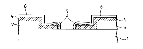
Referring to FIGS. lA and lB, the device comprises
a substrate 1, a pair of device electrodes 2 and 3, an
electroconductive film 4, an electron-emitting region 5
and an oxide coat 6. Note that, in the case of the
device of FIGS. lA and lB, the oxide coat is a layer
formed on the surface of the electroconductive film 4.
As will be described hereinafter, the
electron-emitting region 5 of a device according to the
invention has a configuration schematically illustrated
in one of FIGS. 21A through 21C, although some of the
components of the device are omitted in FIGS. lA, lB,
3, 4D, 5 and 19.
Materials that can be used for the substrate 1
include quartz glass, glass containing impurities such
as Na to a reduced concentration level, soda lime
glass, glass substrate realized by forming an SiO2 layer
on soda lime glass by means of sputtering, ceramic
substances such as alumina as well as Si.
While the oppositely arranged lower and higher
potential side device electrodes 4 and 5 may be made of
any highly conducting material, preferred candidate
materials include metals such as Ni, Cr, Au, Mo, W, Pt,
Ti, Al, Cu and Pd and their alloys, printable
conducting materials made of a metal or a metal oxide
selected from Pd, Ag, Ru02, Pd-Ag and glass, transparent
conducting materials such as In203-SnO2 and
semiconductor materials such as polysilicon.
218~G l~
The distance L separating the device electrodes,
the length W of the device electrodes, the contour of
the electroconductive film 4 and other factors for
designing a surface conduction electron-emitting device
according to the invention may be determined depending
on the application of the device. The distance L
separating the device electrodes is preferably between
hundreds nanometers and hundreds micrometers and, still
preferably, between several micrometers and tens of
several micrometers.
The length W of the device electrodes is
preferably between several micrometers and hundreds of
several micrometers depending on the resistance of the
electrodes and the electron-emitting characteristics of
the device. The film thickness d of the device
electrodes 2 and 3 is between tens of several
nanometers and several micrometers.
A surface conduction electron-emitting device
according to the invention may have a configuration
other than the one illustrated in FIGS. lA and lB and,
alternatively, it may be prepared by sequentially
laying an electroconductive film 4, an oxide coat 6 and
oppositely disposed device electrodes 2 and 3 on a
substrate 1.
The electroconductive film 4 is preferably made of
fine particles in order to provide excellent
21826 47
- 16 -
electron-emitting characteristics. The thickness of
the electroconductive film 4 is determined as a
function of the stepped coverage of the
electroconductive film on the device electrodes 2 and
3, the electric resistance between the device
electrodes 2 and 3 and the parameters for the forming
operation that will be described later as well as other
factors and preferably between hundreds of several
picometers and hundreds of several n~no~eters and more
preferably between a nanometer and fifty nanometers.
The electroconductive film 4 normally shows a sheet
resistance Rs between 102 and 107Q/~. Note that Rs is
the resistance defined by R=Rs(l/w), where t, w and 1
are the thickness, the width and the length of a thin
film respectively and R is the resistance determined
along the longitudinal direction of the thin film.
Note that, while the energization forming operation is
described in terms of current conduction treatment
here, the energization forming operation is not limited
thereto and any operation that can produce one or more
than one fissures in the electroconductive film to give
rise to a region showing a high electric resistance may
suitably be used for the purpose of the invention.
For the purpose of the invention, the
electroconductive film 4 is preferably made of a
material that can give rise to an electron-emitting
region with relatively small power so that it may be
~182647
- 17
covered by a coat of a high melting point metal oxide.
Electroconductive materials that can be used for the
purpose of the invention include Ni, Au, PdO, Pd and
Pt.
The term a "fine particle film" as used herein
refers to a thin film constituted of a large number of
fine particles that may be loosely dispersed, tightly
arranged or mutually and randomly overlapping (to form
an island structure under certain conditions). The
diameter of fine particles to be used for the purpose
of the present invention is between hundreds of several
picometers and hundreds of several nanometers and
preferably between a nanometer and twenty nanometers.
Since the term "fine particle" is frequently used
herein, it will be described in greater depth below.
A small particle is referred to as a "fine
particle" and a particle smaller than a fine particle
is referred to as an "ultrafine particle". A particle
smaller than an "ultrafine particle" and constituted by
several hundred atoms is referred to as a "cluster".
However, these definitions are not rigorous and
the scope of each term can vary depending on the
particular aspect of the particle to be dealt with. An
"ultrafine particle" may be referred to simply as a
"fine particle" as in the case of this patent
application.
"The Experimental Physics Course No. 14:
2182647
- 18 -
Surface/Fine Particle" (ed., Koreo Kinoshita; Kyoritu
Publication, September 1, 1986) describes as follows.
"A fine particle as used herein refers to a
particle having a diameter somewhere between 2 to 3 ,um
and 10 nm and an ultrafine particle as used herein
means a particle having a diameter somewhere between
10 nm and 2 to 3 nm. However, these definitions are by
no means rigorous and an ultrafine particle may also be
referred to simply as a fine particle. Therefore,
these definitions are a rule of thumb in any means. A
particle constituted of two to several hundred atoms is
called a cluster." (Ibid., p. 195, 11.22-26)
Additionally, "Hayashi's Ultrafine Particle
Project" of the New Technology Development Corporation
defines an "ultrafine particle" as follows, employing a
smaller lower limit for the particle size.
"The Ultrafine Particle Project (1981-1986) under
the Creative Science and Technology Promoting Scheme
defines an ultrafine particle as a particle having a
diameter between about 1 and lOOnm. This means an
ultrafine particle is an agglomerate of about 100 to 108
atoms. From the viewpoint of atom, an ultrafine
particle is a huge or ultrahuge particle." (Ultrafine
Particle - Creative Science and Technology: ed.,
Chikara Hayashi, Ryoji Ueda, Akira Tazaki; Mita
Publication, 1988, p. 2, 11.1-4) "A particle smaller
than an ultrafine particle and constituted by several
s~l8~G 47
- 19 -
to several hundred atoms is referred to as a cluster."
(Ibid., p. 2, 11.12-13)
Taking the above general definitions into
consideration, the term "a fine particle" as used
herein refers to an agglomerate of a large number of
atoms and/or molecules having a diameter with a lower
limit between hundreds of several picometers and one
nanometer and an upper limit of several micrometers.
Of the above listed materials that can be used for
the electroconductive film 4, PdO is most suitable
because a fine particle film can easily be formed by
calcining an organic Pd compound in the atmosphere, it
has a relatively low electric conductivity and a wide
process margin relative to the film thickness for
obtaining the above defined resistance Rs since it is a
semiconductor and it can easily be reduced to Pd to
reduce the electric resistance of the electroconductive
film after forming an electron-emitting region.
However, the advantages of the present invention are
not limited by the above listed materials including
PdO.
The electron-emitting region 5 is formed in part
of the electroconductive film 4 and comprises an
electrically highly resistive fissure, although its
performance is dependent on the thickness, the quality
and the material of the electroconductive film 4 and
the energization forming process which will be
- 2 182 6~2~ _
described hereinafter. The electron-emitting region 5
may contain in the inside electroconductive fine
particles with a diameter between hundreds of several
picometers and tens of several nanometers that may be
contain part or all of the elements of the material of
the electroconductive film 4. Additionally, the
electron-emitting region 5 and neighboring areas of the
electroconductive film 4 may contain carbon and/or one
or more than one carbon compounds. Still additionally,
the electron-emitting region 5 may contain part or all
of the elements of the oxide coat 6. Preferably, the
electron-emitting region is made of a material having a
low work function in order to produce a large emission
current.
The metal oxide coat 6 contains one or more than
one oxidized metals as principal ingredient and has a
melting point higher than the material of the
electroconductive film 4. This is to prevent any
degradation of the electron-emitting characteristics of
the electroconductive film 4 due to being molten by
heat and subsequent coagulation of the material of the
electroconductive film 4.
FIGS. 2A through 2C are sectional views
illustrating an electroconductive film 4 covered by a
metal oxide coat 6 in three different possible modes.
A metal oxide coat 6 may be formed in the voids among
the fine particles of the electroconductive film 4 as
~18~6~7
- 21 -
shown in FIG. 2A. Alternatively, a metal oxide coat 6
may be a thin film formed on the electroconductive film
as shown in FIG. 2B. Still alternatively, a metal
oxide coat 6 may be a layer completely covering the
fine particles of the electroconductive film 4 as shown
in FIG. 2C. Note that all the three modes of forming
an metal oxide coat are effective for the purpose of
the invention.
According to the invention, since the
electroconductive film 4 is covered by a metal oxide
coat 6 having a high melting point, the
electroconductive film is prevented from being molten
by heat and subsequently coagulated in areas close to
the electron-emitting region when the electron-emitting
device is driven to operate so that the device can
operate to emit electrons stably for a prolonged period
of time.
When the metal oxide coat 6 is formed in voids
among the fine particles of the electroconductive film
4 as shown in FIG. 2A, the mole percentage of the
metallic elements contained in the metal oxide coat
relative to the metal contained in the
electroconductive film is preferably not higher than
50%. If the mole percentage is greater than 50~, the
electroconductivity of the electroconductive film 4 may
be damaged and the energization forming operation may
require a large power. The mole percentage is
~1826~7 22 -
preferably not smaller than 10~ because, if it is
smaller than 10~, on the other hand, the possible
degradation of the electron-emitting characteristics of
the electroconductive film due to being molten by heat
and subsequent coagulation may not be satisfactorily
suppressed.
When the metal oxide coat is a thin film formed on
the electroconductive film 4 as shown in FIG. 2B, the
thin film preferably has a film thickness not greater
than 20nm. If the metal oxide coat has a thickness
exceeding the above value, it can be electrically
over-charged to change the equipotential surface of the
device and its vicinity when the device is driven to
operate and eventually discharge the electric load to
damage the device. If the energization forming process
is conducted after forming the metal oxide coat, the
power required for the process can become too large to
consequently produce unsatisfactory electron-emitting
characteristics for the device and the process may not
be successfully completed. Additionally, if the
electroconductive film is formed from an
electroconductive oxide and then chemically reduced by
means of reducing gas to lower the electric resistance
of the electroconductive film, the reducing process may
not proceed satisfactory.
The film thickness is preferably not smaller than
lnm because, if the film thickness undergoes the above
21&26 ~ _ 23 -
level, on the other hand, the possible degradation of
the electron-emitting characteristics of the
electroconductive film due to thermal fusion and
subsequent coagulation may not be satisfactorily
suppressed.
When the metal oxide coat 6 is a layer completely
covering the fine particles of the electroconductive
film 4 as shown in FIG. 2C, appropriate values may be
selected for the metal oxide coat so long as the above
two requirements are met. Preferably, the metal oxide
coat has a thickness of 5nm and occupy the voids of the
electroconductive film 4 by about 30~.
Although not shown in FIGS. 2A through 2C, when a
metal oxide coat is formed on the electron-emitting
region 5, a large emission current can be achieved with
a low drive voltage by selecting a metal oxide having a
low work function for the coat.
The work function of the metal oxide coat affects
the performance of the electron-emitting device in many
other ways.
For driving an electron-emitting device to emit
electrons, an anode 54 is arranged to the upstream of
the electron-emitting device as shown in FIG. 6 and a
high voltage is applied to the electron-emitting device
by way of the anode. Then, a complex equipotential
surface appears around the electron-emitting region due
to the low and high potential sides of the
2l8264~
- 24 -
electroconductive film 4 and the anode 54. As
schematically shown in FIG. 19, some of the electrons
emitted from the electron-emitting region 5 leave a
trajectory typically indicated by 2001 before they
directly get to the anode 54, while the remaining
electrons form a trajectory typically indicated by 2002
and strike the high potential side of the
electroconductive film 4. Part of the electrons that
hit the high potential side of the electroconductive
film 4 are elastically reflected and scattered,
typically showing a trajectory indicated by 2003 before
they get to the anode 54, while the others are absorbed
by the electroconductive film 4. The electrons that
get to the anode are observed as emission current Ie
and those that are absorbed by the high potential side
of the electroconductive film 4 are observed as part of
the device electrode If. For an electron-emitting
device to operate efficiently, it preferably shows a
large value for the electron-emission efficiency of
~ = IetIf. In order to have a large electron-emitting
efficiency, more electrons have to be elastically
reflected and scattered out of those that hit the high
potential side of the electroconductive film 4,
typically showing a trajectory as indicated by 2002.
As for an object that elastically reflects and scatters
electrons such as an electroconductive film, the
electron reflectivity of the object is determined not
-` ~1826~
- 25 -
only by the component elements of the object but also
by the work function of the object, which has to be
made small to increase the reflectivity. Thus, the
probability of being elastically scattered for the
electrons emitted from the electron-emitting region
will be increased by covering the electroconductive
film with a substance having a low work function.
Additionally, the metal oxide to be used for the
metal oxide coat 6 is required to show a low vapor
pressure. If the metal oxide produces a high vapor
pressure, the electron-emitting device will be
prevented from operating properly and stably because it
îs driven to operate in vacuum and the metal oxide coat
will be eventually lost as the metal oxide is
evaporated gradually. Generally speaking, the metal
oxide to be used for the metal oxide coat may be
selected from those showing a vapor pressure of about
1.3 x 10~3Pa (lO~sTorr) unless they have a particular
temperature-vapor pressure relationship. When Pd (that
produces a vapor pressure of 1.3 x 10⁻³ at 1370K) is
used for the electroconductive film 4, metal oxides
that can be used for the purpose of the invention
include Al203 (2037K), BeO (1995K), La203 (1690K), TiO2
(1919K), ThO2 (1919K), YzO3 (2234K), HfO2 (2415K), ZrO2
(2203K), BaO (1459K), CaO (1858K), MgO (1714K), SrO
(1687K), FeO (1521K) and WO2 (1783K). (The above oxides
are quoted from p.917 of "Thin Film Handbook" (Ohm
218~6~7
- 26 -
Publishing Co., Ltd.).)
Of these, BeO, CaO, MgO, ThO2, Y203, HfO2, SrO and
ZrO2 are preferably because they have a high melting
point and a low work function. Composite oxide
containing any of the above metals may also be used
effectively for the purpose of the invention. While
some of the metal oxides may be unstable in the
atmosphere and toxic, such instability and toxicity
have nothing to do with the present invention.
Therefore, an appropriate material should be selected
dep~n~;ng on the environment and the purpose of the use
of an electron-emitting device according to the
invention. The metal oxide coat may contain the
carbonate of the metal, its content should be held
below that of the oxide of the metal.
Techniques that can be used to produce a metal
oxide coat comprising a metal oxide as defined above
for the purpose of the invention include vacuum
evaporation (including electron beam evaporation,
resistance heating evaporation and laser evaporation),
sputtering, chemical vapor deposition (CVD), a method
of applying an organic metal compound solution and a
method of forming a deposit of a metal compound by the
Langmuir-Blodgett technique and pyrolyzing it into the
oxide of the metal.
The technique of applying an organic metal
compound solution may be carried out in many different
6 ~ 7
- 27 -
ways. For instance, a solution of metal alkoxide may
be applied to the substrate by simple means such as dip
coating or spin coating. Since metal alkoxide M(OR)x
is soluble into an organic solvent and there are a
number of alkoxide groups that can be combined with a
variety of metals M, this technique can be used to form
a variety of metal oxides and the metal alkoxide
provides suitable materials for the purpose of the
invention.
Since the metal alkoxide is required to be soluble
to the solvent, alcohol ROH having a number of carbon
atoms same as the alkoxide group is typically used.
While most metals can form respective alkoxides, those
that are hardly soluble to the solvent or extremely
reactive are not suitable for the purpose of the
invention. The solubility and reactivity of an
alkoxide group can vary depending on the size of the
group and many alkoxide groups having a small alkyl
group R such as CH3 or C2H5 are insoluble to the
solvent. If a large alkyl group R is involved, on the
other hand, the alkoxide group comprising it may show
an enhanced solvent-solubility but carbon atoms can
remain as impurity in the reaction product after the
pyrolysis. In view of the above facts, the isopropyl
group (iPr), the isobutyl group (iBu), the secondary
butyl group (sBu) and the tertiary butyl group (tBu) are
preferable and the isopropyl group is most preferably
~182~ 4 7
- 28 -
for the purpose of the invention.
The above described application technique is
particularly advantageous because it can be used to
deposit metal oxide without involving the use of a
large vacuum system unlike vacuum evaporation,
sputtering and CVD.
The Langmuir-Blodgett (LB) technique provides
another method for deposing an organic metal compound.
With the LB technique, a monomolecular film is formed
on water by utilizing the hydrophilicity and the
hydrophobicity of both hydrophilic and hydrophobic
molecules and then moved onto the surface of a
substrate so that a monomolecular built-up film (LB
film) can be formed by sequentially laying a number of
monomolecular films on the substrate.
Typical film forming molecules that can be used
for the purpose of the invention include long chain
fatty acids having a hydrophobic group (-CH~-) and a
hydrophilic group (-COOH) in the molecule, of which
those having 16 to 22 carbon atoms are preferable for
forming a monomolecular film on the water/air interface
because of the matching reactivities of the hydrophobic
group and the hydrophilic group within the molecule.
Examples of such long chain fatty acids include
palmitic acid CH3(CH2)14COOH having sixteen carbon atoms,
margaric acid CH3(CH2)1sCOOH having seventeen carbon
atoms, stearic acid CH3(CH2)16COOH having eighteen carbon
~ 18~6~i
-
- 29 -
atoms, nonadecaic acid CH3(CH2)17COOH having nineteen
carbon atoms, arachidic acid CH3(CH2)18COOH having twenty
carbon atoms, heneicosaic acid CH3(CH2)19COOH having
twenty one carbon atoms and behenic acid CH3(CH2)20COOH
having twenty two carbon atoms. Typically, a selected
one of these fatty acids is dissolved to a volatile
solvent such as chloroform or benzene to a
concentration of 0.5 to 5.0 mM/liter and caused to fall
dropwise on the water surface to give rise to a
monomolecular film.
- Various metal salts of these fatty acids can also
be used for forming a film by means of the LB
technique. For forming such a monomolecular film, a
fatty acid solution is made to spread on the surface of
the underlying water that contains metal ions to a
concentration of 0.001 mM/liter to 5.0 mM/liter. While
a monomolecular film of the salt of a metal having a
relatively large valence, for example the aluminum salt
of fatty acid where the aluminum is trivalent, is
stable, such a film cannot be produced by an ordinary
LB technique because of the film shows an enormous
rigidity. If such is the case, a moving wall type
(Miyata type) trough will provide a mighty help for
forming a film. The ordinary LB technique is typically
used with an apparatus as illustrated in FIGS. 20A and
20B, where the substrate is moved vertically to
sequentially form monomolecular films thereon. As more
21826~
- 30 -
films are formed, the float is moved to reduce the
developed surface area of the monomolecular film on the
water in order to maintain the surface pressure to a
constant level. With the moving wall technique, on the
other hand, the substrate has a width equal to that of
the trough and the peripheral walls of the trough moves
to reduce the developed surface area of the
monomolecular film on the water as the substrate is
moved vertically to pick up the film onto the
substrate.
Normally, a metal salt of fatty acid is good for
forming monomolecular films when the metal is selected
from divalent metals such as Cd, Ca and Ba. An LB film
of any of such metal salts of fatty acid can be
produced by means of the ordinary LB technique. If a
monovalent metal is used, it can form a micelle to
eventually dissolved into water.
Compounds that can be used for forming an LB film
by the LB technique are not limited to fatty acids so
long as they have both a hydrophilic group and a
hydrophoblc group within a molecule. Examples of
compounds that can be used with the LB technique to
form a film include long chain amines (such as
octadecile amine) having both an hydrophobic group
(-CHn-) and a hydrophilic group (-NH2-) and polymers
(e.g., polyimides) having both a hydrophobic group and
a hydrophilic group that show matching reactivities.
~1826~7
- 31 -
If such an organic compound maintains its
hydrophobicity and hydrophilicity when it is made to
contain a metal in the form of salt or complex, a film
of the oxide of the metal can be produced by
sequentially forming monomolecular films of the organic
compound that contains the metal and pyrolyzing the
obtained built-up film as the hydrocarbon is decomposed
and volatilized. Amm et al. produced yttrium oxide and
cadmium oxide by forming built-up films of yttrium
arachidate and cadmium arachidate and pyrolyzing the
respective films [D. T. Amm, D. J. Johnson, T. Laursen
and S. K. Gupta. Appl. Phys. Lett. 61,522, (1992) and
D. T. Amm, D. J. Johnson, N. Matsuura, T. Laursen and
G. Palmer, Thin Solid Films, 242,74, (1994)]. Taylor
and et al. synthetically produced zinc oxide by
pyrolyzing a built-up film of zinc stearate [D. M.
Taylor and J. N. Lambi, Thin Solid Films, 243,384,
(1994)].
According to the invention, a metal oxide coat 6
is formed on an electroconductive film 4 by applying
the above method of synthetically producing oxides of
metals. More specifically, a desired number of
monomolecular films of a metal salt of fatty acid or a
long chain amine/metal complex are sequentially laid on
a substrate and then pyrolyzed to produce a metal oxide
layer having a desired film thickness. This method is
particularly advantageous to accurately controlling the
~ ~826 ~7
- 32 -
film thickness of the metal oxide layer.
For using the LB technique, care should be taken
to control the pH value of the underlying water on
which a monomolecular film is spread and the pH
regulating agent (buffer solution) to be used with it.
The formation of a metal salt of fatty acid is heavily
dependent on the pH value of the reaction system and
the latter varies depending on the metal involved. A
low ratio of the total number of molecules of the
developed fatty acid to the number of molecules that
have formed the metal salt is not favorable because,
the lower the ratio, the lower is the concentration of
the metal in the built-up film and hence that of the
formed metal oxide. The pH value of the underlying
water should be selected depending on the involved
metal. While phosphate, borate and carbonate are
popularly used for buffer solutions, the use of a
buffer solution that does not contain any metal is
preferable for the purpose of the invention because, if
it does contain metal, the metal and the developed
fatty acid easily and undesirably react with each other
to produce a metal salt. Additionally, the use of an
organic compound type buffer solution is preferable in
order to avoid the generation of corrosive gas after
the pyrolysis. Organic compounds that are preferably
used for the purpose of the invention include
tri(hydroxymethyl)aminomethane, glycine and acetic
~1~26~7
.
- 33 -
acid, although other compounds that do not adversely
affect the pyrolysis may also be used. The process of
producing a metal oxide coat on a substrate carrying
thereon an electroconductive film 4 specifically
proceeds as follows.
Firstly, the substrate on which an
electroconductive film 4 has been formed is
preliminarily treated for hydrophobicity before forming
an LB film. While known techniques for treating the
surface of a substrate for hydrophobicity include the
vapor phase adsorption technique involving the use of
hex~rethyldisilazane and the technique of forming a
single layer of octadecileamine film by means of the LB
method, any other appropriate techniques for treating
the surface of a substrate for hydrophobicity may also
be used for the purpose of the invention. If the
substrate is significantly stained, the stain may have
to be removed typically by means of a W/03 treatment
that is popularly used in the semiconductor process to
make it hydrophilic in advance. Then, layers of a
metals salt of fatty acid or those of a long chain
mine/metal complex are formed on the preliminarily
treated substrate is by means of the LB technique. As
described above, fatty acids that can be used for the
purpose of the invention include those having 16 to 22
carbon atoms. Long chain amines that can be used for
the purpose of the invention include their isomers.
~l82647
- 34 -
Metal compounds that can be used for the purpose of the
present invention include chlorides and acetates of Mg,
Ca, Ba, Y, Al and Ti. The concentration of the
dissolved metal is typically between 0.01 mM/liter and
10 mM/liter. As described above, the pH value of the
underlying water have to be regulated by means of an
appropriate buffer solution in order to accelerate the
formation of a metal salt. The obtained built-up film
of the metal salt of fatty acid is then thermally
treated at 300 to 600C for 20 to 60 minutes in the
atmosphere to produce a metal oxide coat 6.
On the other hand, most of the above listed high
melting point metal oxides are electrically insulating.
When the electroconductive film 4 and the
electron-emitting region 5 are covered by a
considerably thick electrically insulating metal oxide
film, it can obstruct the emission of electrons from
the electron-emitting region to adversely affect the
performance of the electron-emitting device.
Additionally, as described earlier, the
electroconductive film can be electrically overcharged
by electronrons emitted from the electron-emitting
region and striking the film to give rise to problems
during the operation of the device.
The metal oxide may be made electroconductive by
doping it with alkaline metal or alkaline earth metal
but such induced electroconductivity can become
~l826~7
- 35 -
unstable when it is exposed to high temperature in
vacuum.
If an electroconductive metal oxide is used, the
electroconductivity of the produced metal oxide coat
can become unnegligible relative to the
electroconductivity of the electroconductive film to
consequently consume large power for the process of
energization forming.
In view of the above problems, the metal oxide
coat 6 may well have a thickness between lnm and 20nm
if it is electrically insulating. If the thickness is
found within the above defined range, the metal oxide
coat does not adversely affect the operation of the
electron-emitting device and operates effectively to
suppress any possible degradation of the performance of
the device. It should be noted, however, that the
above cited parameters are not necessarily absolute and
may be modified depending on the form and the density
of the metal oxide and other conditions.
Now, a step type electron-emitting device will be
described below.
FIG. 3 is a schematic cross sectional view of a
step type electron-emitting device according to the
invention.
In FIG. 3, the components that are same as or
similar to those of the device of FIGS. lA and lB are
denoted by the same reference symbols. Reference
~l8~6 4 l
- 36 -
symbol 21 denotes a step-forming section. The device
comprises a substrate 1, device electrodes 2 and 3,
electroconductive thin film 4 and an electron emitting
region 5, which are made of materials same as a flat
type surface conduction electron-emitting device as
described above, as well as a step-forming section 21
made of an insulating material such as SiO2 produced by
vacuum deposition, printing or sputtering and having a
height corresponding to the distance L separating the
device electrodes of a flat type surface conduction
electron-emitting device as described above, or between
several hundred n~no~ters and tens of several
micrometers. Preferably, the height of the
step-forming section 21 is between tens of several
nanometers and several micrometers, although it is
selected as a function of the method of producing the
step-forming section used there and the voltage to be
applied to the device electrodes.
After forming the device electrodes 2 and 3 and
the step-forming section 21, the electroconductive thin
film 4 is laid on the device electrodes 2 and 3. While
the electron-emitting region 5 is formed on the
step-forming section 21 in FIG. 3, its location and
contour are dependent on the conditions under which it
is prepared, the energization forming conditions and
other related conditions are not limited to those shown
there.
~l82647
- 37 -
While various methods may be conceivable for
manufacturing a surface conduction electron-emitting
device having a configuration illustrated in FIGS. lA
and lB. FIGS. 4A through 4D schematically illustrate a
typical one of such methods. Note that, in FIGS. 4A
through 4D, the components that are same as or similar
to those of the device of FIGS. lA and lB are denoted
by the same reference symbols.
1) After thoroughly cleansing a substrate 1 with
detergent, pure water and organic solvent, a material
is deposited on the substrate 1 by means of vacuum
deposition, sputtering or some other appropriate
technique for a pair of device electrodes 2 and 3,
which are then produced by photolithography (FIG. 4A).
2) An organic metal thin film is formed on the
substrate 1 that carries thereon the pair of device
electrodes 2 and 3 by applying an organic metal
solution and leaving the applied solution for a given
period of time. The organic metal solution may contain
as principal ingredient any of the metals listed
earlier for the electroconductive thin film 4.
Thereafter, the organic metal thin film is heated,
calcined and subsequently subjected to a patterning
operation, using an appropriate technique such as
lift-off or etching, to produce an electroconductive
thin film 4 (FIG. 4B). While an organic metal solution
is used to produce thin films in the above description,
~182647
- 38 -
an electroconductive thin film 4 may alternatively be
formed by vacuum deposition, sputtering, chemical vapor
phase deposition (CVD), dispersed application, dipping,
spinner or some other technique.
3) Then, a metal oxide coat 6 is formed on the
substrate 1 that carriers thereon the electroconductive
film 4 by means of electron beam evaporation, using a
metal oxide having a melting point higher than that of
the material of the electroconductive film 4 as the
material to be evaporated (FIG. 4C). While the metal
oxide is the principal ingredient of the formed metal
oxide coat 6, the latter may additionally contain the
metal carbonate or hydroxide as part of it. Note that,
however, such metal carbonate or hydroxide that may be
used for the purpose of the invention does not provide
any problem because, when heated, it is changed to the
corresponding oxide and the melting point (or
sublimating point) of the oxide is important for the
operation of the prepared electron-emitting device.
For the purpose of the invention, the metal oxide coat
6 may well cover or be contained in the
electroconductive film 4 and does not need to be
specifically patterned unless it is highly
electroconductive, although it may be formed with the
electroconductive film 4 before the latter is subjected
to a patterning operation described above for the
second processing step so that both the
~182~ ~
- 39 -
electroconductive film 4 and the metal oxide coat 6 may
be patterned simultaneously and appropriately. It may
be needless to say that any areas of the device to be
used for electrically connecting the device electrodes
2 and 3 and a power source or a drive circuit (not
shown) should not be covered by the metal oxide coat 6.
The technique to be used for forming the metal
oxide coat 6 is not limited to electron beam
evaporation and may be selected from other techniques
including vacuum evaporation, sputtering and CVD. In
the case of manufacturing an electron source having a
large surface area, a film of an organic metal compound
may be formed by applying the solution of the compound
or by means of the LB technique and subsequently
heat-treating the solution. Note that the metal oxide
coat 6 may be formed after the energization forming
process as will be described hereinafter by using a
material and processing procedures that are selected
appropriately.
4) Subsequently, the device is subjected to a
process referred to as "energization forming". While
energization forming is described below in terms of
current conduction treatment, any appropriate technique
for forming a gap in the electroconductive film 4 to
produce an electrically highly resistive condition may
alternatively be used for the energization forming
process for the purpose of the invention.
~182~47
- 40 -
An electric current is conducted between the
device electrodes 2 and 3 by means of a power source
(not shown) to produce an electron-emitting region 5 in
the electroconductive film by structuring modifying the
latter (FIG. 4D). As a result of energization forming,
part of the electroconductive thin film 3 is locally
destroyed, deformed or transformed to make an
electron-emitting region 5. If a metal oxide coat 6 is
formed before the energization forming process, it may
also be locally destroyed, deformed or transformed.
Voltage waveforms that can be used for
energization forming are shown in FIGS. 5A and 5B.
The voltage to be used for energization forming
preferably has a pulse waveform. A pulse voltage
having a constant height or a constant peak voltage may
be applied continuously as shown in FIG. 5A or,
alternatively, a pulse voltage having an increasing
wave height or an increasing peak voltage may be
applied as shown in FIG. 5B.
In FIG. 5A, the pulse voltage has a pulse width T1
and a pulse interval T2, which are typically between
1 ~usec. and 10 msec. and between 10 ,usec. and 100 msec.
respectively. The height of the triangular wave (the
peak voltage for the energization forming operation)
may be appropriately selected depending on the profile
of the surface conduction electron-emitting device.
Such a voltage is applied to the device electrodes for
21826~7
_ - 41 -
several seconds to tens of several minutes typically in
vacuum of a degree of 1.3 x 10~3Pa or less. Note that
the waveform of the pulse is not necessarily limited to
triangle and a rectangular or some other waveform may
also be used. Also note that the pulse waveheight, the
pulse width and the pulse interval are not limited to
the above values and any other appropriate values may
alternatively be selected to produce an
electron-emitting region in good shape.
FIG. 5B shows a pulse voltage whose pulse height
increases with time. In FIG. 5B, the pulse voltage has
an width Tl and a pulse interval T2 that are
substantially similar to those of FIG. 5A. The height
of the triangular wave (the peak voltage for the
energization forming operation) is, however, gradually
increased.
The energization forming operation will be
terminated by measuring the current running through the
device electrodes when a voltage that is sufficiently
low and cannot locally destroy or deform the
electroconductive thin film 4, or about 0.1 V, is
applied to the device during an interval T2 of the
pulse voltage. Typically the energization forming
operation is terminated when a resistance greater than
lM ohms is observed for the device current running
through the electroconductive film 3 while applying a
voltage of approximately 0.1 V to the device electrodes.
~1~264~
5) Thereafter, the device is subjected to an
activation process. An activation process is a process
by means of which the device current If and the
emission current Ie are changed remarkably.
In an activation process, a pulse voltage may be
repeatedly applied to the device in an atmosphere of
the gas of an organic substance as in the case of
energization forming process. The atmosphere may be
produced by utilizing the organic gas remaining in a
vacuum chamber after evacuating the chamber by means of
an oil diffusion pump or a rotary pump or by
sufficiently evacuating a vacuum chamber by means of an
ion pump and thereafter introducing the gas of an
organic substance into the vacuum. The gas pressure of
the organic substance is determined as a function of
the profile of the electron-emitting device to be
treated, the profile of the vacuum chamber, the type of
the organic substance and other factors. Organic
substances that can be suitably used for the purpose of
the activation process include aliphatic hydrocarbons
such as alkanes, alkenes and alkynes, aromatic
hydrocarbons, alcohols, aldehydes, ketones, amines,
organic acids such as, phenol, carbonic acids and
sulfonic acids. Specific examples include saturated
hydrocarbons expressed by general formula CnH2n+2 such as
methane, ethane and propane, unsaturated hydrocarbons
expressed by general formula CnH2n such as ethylene and
~18 2 6 -1 ~
- 43 -
propylene, benzene, toluene, methanol, ethanol,
formaldehyde, acetaldehyde, acetone, methylethylketone,
methylamine, ethylamine, phenol, formic acid, acetic
acid and propionic acid. As a result of an activation
process, carbon or a carbon compound is deposited on
the device out of the organic substances existing in
the atmosphere to remarkably change the device current
If and the emission current Ie.
The order of carrying out the step of forming a
metal oxide coat and that of forming a deposited film
of carbon or a carbon compound by an activation process
may be reversed depending on which layer comes upper on
the prepared device.
Since a voltage is applied between the device
electrodes in the activation process as described
above, coagulation may take place, if slightly, during
this process to consequently reduce the emission
current Ie if it is conducted before the formation of a
metal oxide coat, although such reduction in the
emission current is very small. Since the metal oxide
coat is located above the deposit of carbon or a carbon
compound, on the other hand, the effect of improving
the electron emission efficiency can become conspicuous
if the metal oxide coat has a low work function. To
the contrary, when the activation process comes after
the film formation, any slight reduction in the
emission current due to the activation process can be
~1826 l I
- 44 -
effectively prevented.
The time of terminating the activation process is
determined appropriately by observing the device
current If and the emission current Ie. The pulse
width, the pulse interval and the pulse wave height of
the pulse voltage to be used for the activation process
will be appropriately selected.
For the purpose of the invention, carbon and
carbon compounds include graphite (namely HOPG, PG and
GE, of which HOPG has a substantially perfect graphite
crystalline structure and PG has a somewhat distorted
crystalline structure with an average crystal grain
size of 20 nanometers, while the crystalline structure
of GC is further distorted with an average crystal
grain size as small as 2 n~nometers) and noncrystalline
carbon (refers to amorphous carbon and a mixture of
amorphous carbon and fine crystal grains of graphite)
and the thickness of the deposited film is preferably
less than 50 nanometers, more preferably less than
30 nanometers.
6) An electron-emitting device that has been
treated in an energization forming process and an
activation process is then preferably subjected to a
stabilization process. This is a process for removing
any organic substances remaining in the vacuum chamber.
The vacuuming and exhausting equipment to be used for
this process preferably does not involve the use of oil
~182~l~7
-- - 45 -
so that it may not produce any evaporated oil that can
adversely affect the performance of the performance of
the treated device during the process. Thus, the use
of a sorption pump or an ion pump may be a preferable
choice.
If an oil diffusion pump or a rotary pump is used
for the activation process and the organic gas produced
by the oil is also utilized, the partial pressure of
the organic gas has to be minimized by any means. The
partial pressure of the organic gas in the vacuum
chamber is preferably lower than 1.3 x 10~6Pa and more
preferably lower than 1.3 x 10~8Pa if no carbon or
carbon compound is additionally deposited. The vacuum
chamber is preferably evacuated after heating the
entire chamber so that organic molecules adsorbed by
the inner walls of the vacuum chamber and the
electron-emitting device in the chamber may also be
easily eliminated. While the vacuum chamber is
preferably heated to 80C or above, preferably to 250C
or above, for as long as possible, other heating
conditions may alternatively be selected depending on
the size and the profile of the vacuum chamber and the
configuration of the electron-emitting device in the
chamber as well as other considerations. The pressure
in the vacuum chamber needs to be made as low as
possible and it is preferably lower than 1 x lO~sPa and
more preferably lower than 1.3 x 10~6Pa, although some
218~6 i7
- 46 -
other level of pressure may appropriately be selected.
After the stabilization process, the atmosphere
for driving the electron-emitting device or the
electron source is preferably same as the one when the
stabilization process is completed, although a lower
pressure may alternatively be used without damaging the
stability of operation of the electron-emitting device
or the electron source if the organic substances in the
chamber are sufficiently removed.
By using such a low pressure atmosphere, the
formation of any additional deposit of carbon or a
carbon compound can be effectively suppressed and H20,
2 and other substances that have been adsorbed by the
vacuum chamber and the substrate can be effectively
removed to consequently stabilize the device current If
and the emission current Ie.
The performance of a surface conduction
electron-emitting device prepared by way of the above
processes will be described below referring to FIGS. 6
and 7A.
FIG. 6 is a schematic block diagram of an
arrangement comprising a vacuum chamber that can also
be used as a gauging system for determining the
performance of an electron emitting device of the type
under consideration. Referring to FIG. 6, those
components that are similar to or same as those of
FIGS. lA and lB are denoted by the same reference
6~182~ ~7
- - 47 -
symbols. The gauging system includes a vacuum chamber
S5 and a vacuum pump 56. An electron-emitting device
is placed in the vacuum chamber 55. The device
comprises a substrate 1, a pair of device electrodes 2
and 3, an electroconductive film 4 and an
electron-emitting region 5. Otherwise, the gauging
system has a power source 51 for applying a device
voltage Vf to the device, an ammeter 50 for metering
the device current If running through the
electroconductive film 4 between the device electrodes
2 and 3, an anode 54 for capturing the emission current
Ie produced by electrons emitted from the
electron-emitting region of the device, a high voltage
source 53 for applying a voltage to the anode 54 of the
gauging system and another ammeter 52 for metering the
emission current Ie produced by electrons emitted from
the electron-emitting region 5 of the device. For
determining the performance of the electron-emitting
device, a voltage between 1 and 10 KV may be applied to
the anode, which is spaced apart from the electron
emitting device by distance H which is between 2 and
8 mm.
The surface conduction electron-emitting device
and the anode 54 and other components are arranged in
the vacuum chamber 55, which is equipped with a vacuum
gauge and other necessary instruments so that the
performance of the electron-emitting device in the
21826 1~
-
- 48 -
chamber may be properly tested in vacuum of a desired
degree. The vacuum pump 56 may be provided with an
ordinary high vacuum system comprising a turbo pump or
a rotary pump an ultra-high vacuum system comprising an
ion pump. The entire vacuum chamber 55 and the
substrate of an electron-emitting device contained
therein can be heated by means of a heater (not shown).
Thus, this vacuum processing arrangement can be used
for an energization forming process and the subsequent
processes.
FIG. 7A shows a graph schematically illustrating
the relationship between the device voltage Vf and the
emission current Ie and the device current If typically
observed by the gauging system of FIG. 6. Note that
different units are arbitrarily selected for Ie and If
in FIG. 7A in view of the fact that Ie has a magnitude
by far smaller than that of If. Note that both the
vertical and transversal axes of the graph represent a
linear scale.
As seen in FIG. 7A, an electron-emitting device
according to the invention has three remarkable
features in terms of emission current Ie, which will be
described below.
(i) Firstly, an electron-emitting device according
to the invention shows a sudden and sharp increase in
the emission current Ie when the voltage applied
thereto exceeds a certain level (which is referred to
~1~2~ 17
- 49 -
as a threshold voltage hereinafter and indicated by Vth
in FIG. 7A), whereas the emission current Ie is
practically undetectable when the applied voltage is
found lower than the threshold value Vth. Differently
stated, an electron-emitting device according to the
invention is a non-linear device having a clear
threshold voltage Vth to the emission current Ie.
(ii) Secondly, since the emission current Ie is
highly dependent on the device voltage Vf, the former
can be effectively controlled by way of the latter.
(iii) Thirdly, the emitted electric charge
captured by the anode 54 is a function of the duration
of time of application of the device voltage Vf. In
other words, the amount of electric charge captured by
the anode 54 can be effectively controlled by way of
the time during which the device voltage Vf is applied.
Because of the above remarkable features, it will
be understood that an electron-emitting device
according to the invention can be easily controlled for
its electron-emitting performance as a function of
input signal. Therefore, such an electron-emitting
device may various applications including an electron
source realized by arranging a plurality of
electron-emitting devices and an image-forming
apparatus comprising such an electron source.
The device current If either monotonically
increases relative to the device voltage Vf as shown by
- ~1826~t
- 50 -
a solid line in FIG. 7A (a characteristic referred to
as "MI characteristic" hereinafter) or changes to show
a curve (not shown) specific to a
voltage-controlled-negative-resistance characteristic
(a characteristic referred to as "VCNR characteristic"
hereinafter, although it is not illustrated). These
characteristics of the device current are dependent on
a number of factors including the manufacturing method,
the conditions where it is gauged and the environment
for operating the device. Note that, if the device
current If shows a VCNR characteristic relative to the
device voltage Vf, the emission current Ie shows an MI
characteristic to the device voltage Vf.
FIG. 8 schematically shows the change with time in
the emission current when an electron-emitting device
according to the invention is driven to operate by
applying a constant pulse voltage to the device. In
FIG. 8, the solid line indicates the performance of the
device of the invention and the broken line shows that
of a comparable device that does not carry any metal
oxide coat. It is clear from FIG. 8 that a high level
of electron-emitting performance is sustained with an
electron-emitting device according to the invention.
It may be safe to assume that this sustained
performance is the net result of the arrangement of a
metal oxide coat 6 that suppresses any degradation of
the electroconductive film 4 due to coagulation of the
- ~1826~7
- 51 -
substance of the electroconductive film 4 in and near
the electron-emitting region 5.
Because of the remarkable features of an
electron-emitting device according to the invention,
the electron-emitting behavior of an electron source
comprising a plurality of electron-emitting devices
according to the invention and hence that of an
image-forming apparatus incorporating such an electron
source can easily be controlled as a function of input
signal and provide clear images because the
electron-emitting devices can emit electrons for a
prolonged period of time on a stable basis. Thus, such
an electron source and an image-forming apparatus may
find a variety of applications.
Now, some examples of the usage of
electron-emitting devices, to which the present
invention is applicable, will be described. According
to the invention, an electron source can be realized by
arranging a plurality of electron-emitting devices.
Electron-emitting devices may be arranged on a
substrate in a number of different modes.
For instance, a number of electron-emitting
devices may be arranged in parallel rows along a
direction (hereinafter referred to row-direction), each
device being connected by wires as at opposite ends
thereof, and driven to operate by control electrodes
(hereinafter referred to as grids) arranged in a space
- 21~264~
- 52 -
above the electron-emitting devices along a direction
perpendicular to the row direction (hereinafter
referred to as column-direction) to realize a
ladder-like arrangement. Alternatively, a plurality of
electron-emitting devices may be arranged in rows along
an X-direction and columns along an Y-direction to form
a matrix, the X- and Y-directions being perpendicular
to each other, and the electron-emitting devices on a
same row are connected to a common X-directional wire
by way of one of the electrodes of each device while
the electron-emitting devices on a same column are
connected to a common Y-directional wire by way of the
other electrode of each device. The latter arrangement
is referred to as a simple matrix arrangement. Now,
the simple matrix arrangement will be described in
detail.
In view of the above described three basic
characteristic features (i) through (iii) of a surface
conduction electron-emitting device, to which the
invention is applicable, it can be controlled for
electron emission by controlling the wave height and
the wave width of the pulse voltage applied to the
opposite electrodes of the device above the threshold
voltage level. On the other hand, the device does not
practically emit any electron below the threshold
voltage level. Therefore, regardless of the number of
electron-emitting devices arranged in an apparatus,
~182~47
- 53 -
desired surface conduction electron-emitting devices
can be selected and controlled for electron emission in
response to an input signal by applying a pulse voltage
to each of the selected devices.
FIG. 9 is a schematic plan view of the substrate
of an electron source realized by arranging a plurality
of electron-emitting devices, to which the present
invention is applicable, in order to exploit the above
characteristic features. In FIG. 9, the electron
source comprises an electron source substrate 1, which
is a glass substrate as described above and the number
and the configuration of the electron-emitting devices
104 arranged on the substrate 1 may be determined
depending on the application of the electron source.
There are provided a total of m X-directional
wires 102, which are donated by Dxl, Dx2, ..., Dxm and
made of an electroconductive metal produced by vacuum
deposition, printing or sputtering. These wires are so
designed in terms of material, thickness and width
that, if necessary, a substantially equal voltage may
be applied to the surface conduction electron-emitting
devices. A total of n Y-directional wires 103 are
arranged and donated by Dyl, Dy2, ..., Dyn, which are
similar to the X-directional wires 102 in terms of
material, thickness and width. An interlayer
insulation layer (not shown) is disposed between the m
X-directional wires 102 and the n Y-directional wires
21826 1~
- 54 -
103 to electrically isolate them from each other. Both
m and n are integers.
The interlayer insulation layer (not shown) is
typically made of SiO2 and formed on the entire surface
or part of the surface of the insulating substrate 1 to
show a desired contour by means of vacuum deposition,
printing or sputtering. For example, it may be formed
on the entire surface or part of the surface of the
substrate 1 on which the X-directional wires 102 have
been formed. The thickness, material and manufacturing
method of the interlayer insulation layer are so
selected as to make it withstand the potential
difference between any of the X-directional wires 102
and any of the Y-directional wires 103 observable at
the crossing thereof. Each of the X-directional wires
102 and the Y-directional wires 103 is drawn out to
form an external terminal.
The oppositely arranged paired electrodes (not
shown) of each of the surface conduction
electron-emitting devices 104 are connected to related
one of the m X-directional wires 102 and related one of
the n Y-directional wires 103 by respective connecting
wires 105 which are made of an electroconductive metal.
The electroconductive metal material of the device
electrodes and that of the connecting wires 105
extending from the wire 102 and 103 may be same or
contain a common element as an ingredient.
- ~1826~7
Alternatively, they may be different from each other.
These materials may be appropriately selected typically
from the candidate materials listed above for the
device electrodes. If the device electrodes and the
connecting wires are made of a same material, they may
be collectively called device electrodes without
discriminating the connecting wires. Note that the
electron-emitting devices 104 may be formed either on
the substrate 1 or on an interlayer insulation layer
(not shown).
The X-directional wires 102 are electrically
connected to a scan signal application means (not
shown) for applying a scan signal to a selected row of
surface conduction electron-emitting devices 104.
On the other hand, the Y-directional wires 103 are
electrically connected to a modulation signal
generation means (not shown) for applying a modulation
signal to a selected column of surface conduction
electron-emitting devices 104 and modulating the
selected column according to an input signal. Note
that the drive signal to be applied to each surface
conduction electron-emitting device is expressed as the
voltage difference of the scan signal and the
modulation signal applied to the device.
Now, an image-forming apparatus comprising an
electron source having a simple matrix arrangement as
described above will be described by referring to FIGS.
- ~l826~7- 56 -
10 through 12. FIG. 10 is a partially cut away
schematic perspective view of the image forming
apparatus and FIGS. llA and llB show two possible
configurations of a fluorescent film that can be used
for the image forming apparatus of FIG. 10, whereas
FIG. 12 is a block diagram of a drive circuit for the
image forming apparatus of FIG. 10 that operates for
NTSC television signals.
Referring firstly to FIG. 10 illustrating the
basic configuration of the display panel of the
image-forming apparatus, it comprises an electron
source substrate 1 of the above described type carrying
thereon a plurality of electron-emitting devices, a
rear plate 111 rigidly holding the electron source
substrate 1, a face plate 116 prepared by laying a
fluorescent film 114 and a metal back 115 on the inner
surface of a glass substrate 113 and a support frame
112, to which the rear plate 111 and the face plate 116
are bonded by means of frit glass. Reference numeral
118 denotes an envelope, which is baked to 400 to 500C
for more than 10 minutes in the atmosphere or in
nitrogen and hermetically and airtightly sealed.
In FIG. 10, reference numerals 102 and 103
respectively denotes X- and Y-directional wires, each
being connected to the paired device electrodes 2 and 3
of the related electron-emitting devices 104 and
provided with the appropriate one of external terminals
~ ~ 8 2 6 i ~
- 57
Dxl through Dxm and Dyl through Dyn.
While the envelope 118 is formed of the face plate
116, the support frame 112 and the rear plate 111 in
the above described embodiment, the rear plate 111 may
be omitted if the substrate 1 is strong enough by
itself because the rear plate 111 is provided mainly
for reinforcing the substrate 1. If such as the case,
an independent rear plate 111 may not be required and
the substrate 1 may be directly bonded to the support
frame 112 so that the envelope 118 is constituted of a
face plate 116, a support frame 112 and a substrate 1.
The overall strength of the envelope 118 may be
increased by arranging a number of support members
called spacers (not shown) between the face plate 116
and the rear plate 1.
While the fluorescent film 114 may comprise only a
single fluorescent body if the display panel is used
for showing black and white pictures, it needs to
comprise for displaying color pictures black conductive
members 121 and fluorescent bodies 122, of which the
former are referred to as black stripes (FIG. llA) or
members of a black matrix (FIG. llB) depending on the
arrangement of the fluorescent bodies. Black stripes
or members of a black matrix are arranged for a color
display panel so that the fluorescent bodies 122 of
three different primary colors are made less
discriminable and the adverse effect of reducing the
~82~ ~ ~
- 58 -
contrast of displayed images of external light
reflected by the fluorescent film 114 is weakened by
blackening the surrounding areas. While graphite is
normally used as a principal ingredient of the black
stripes, other conductive material having low light
transmissivity and reflectivity may alternatively be
used.
A precipitation or printing technique is suitably
be used for applying a fluorescent material on the
glass substrate 113 regardless of black and white or
color display. An ordinary metal back 115 is arranged
on the inner surface of the fluorescent film 114. The
metal back 115 is provided in order to enhance the
luminance of the display panel by causing the rays of
light emitted from the fluorescent bodies and directed
to the inside of the envelope to turn back toward the
face plate 116, to use it as an electrode for applying
an accelerating voltage to electron beams and to
protect the fluorescent bodies against damages that may
be caused when negative ions generated inside the
envelope collide with them. It is prepared by
smoothing the inner surface of the fluorescent film (in
an operation normally called "filming") and forming an
Al film thereon by vacuum deposition after forming the
fluorescent film.
A transparent electrode (not shown) may be formed
on the face plate 116 facing the outer surface of the
- ~L&~6 i7
- 59 -
fluorescent film 114 in order to raise the conductivity
of the fluorescent film 114.
Care should be taken to accurately align each set
of color fluorescent bodies and an electron-emitting
device, if a color display is involved, before the
above listed components of the envelope are bonded
together.
The envelope 118 is evacuated by way of an exhaust
pipe (not shown), using an oil free exhaust system
typically comprising an ion pump and a sorption pump,
while heating the inside appropriately as in the case
of the above described stabilizing process to be
conducted on each electron-emitting device, until the
atmosphere in the inside is reduced to a degree of
vacuum of lO~sPa containing organic substances to a very
low concentration, when it is hermetically sealed,
while being heated appropriately as in the case of the
above described stabilization process. A getter
process may be conducted in order to maintain the
achieved degree of vacuum in the inside of the envelope
118 after it is sealed. In a getter process, a getter
arranged at a predetermined position (not shown) in the
envelope 118 is heated by means of a resistance heater
or a high frequency heater to form a film by vapor
deposition immediately before or after the envelope 118
is sealed. A getter typically contains Ba as a
principal ingredient and can maintain a degree of
- - -
h 18 ~ ~ ~7
- -- 60 --
vacuum between 10-3 and 10-5 by the adsorption effect of
the vapor deposition film.
The processes of manufacturing surface conduction
electron-emitting devices of the image forming
apparatus after the forming process may appropriately
be designed to meet the specific requirements of the
intended application.
Now, a drive circuits for driving a display panel
comprising an electron source with a simple matrix
arrangement for displaying television images according
to NTSC television signals will be described by
referring to Fig. 12. In Fig. 12, reference numeral
201 denotes an image-forming apparatus. Otherwise, the
circuit comprises a scan circuit 202, a control circuit
203, a shift register 204, a line memory 205, a
synchronizing signal separation circuit 206 and a
modulation signal generator 207. Vx and Va in Fig. 12
denote DC voltage sources.
The image-forming apparatus 201 is connected to
external circuits via terminals Dxl through Dxm, Dyl
through Dym and high voltage terminal Hv, of which
terminals Dxl through Dxm are designed to receive scan
signals for sequentially driving on a one-by-one basis
the rows (of n devices) of an electron source in the
apparatus comprising a number of surface-conduction
type electron-emitting devices arranged in the form of
a matrix having m rows and n columns.
218~6 ~q
- 61 -
On the other hand, terminals Dyl through Dyn are
designed to receive a modulation signal for controlling
the output electron beam of each of the
surface-conduction type electron-emitting devices of a
row selected by a scan signal. High voltage terminal
Hv is fed by the DC voltage source Va with a DC voltage
of a level typically around lOkV, which is sufficiently
high to energize the fluorescent bodies of the selected
surface-conduction type electron-emitting devices.
The scan circuit 202 operates in a manner as
follows. The circuit comprises M switching devices (of
which only devices Sl and Sm are specifically indicated
in Fig. 13), each of which takes either the output
voltage of the DC voltage source Vx or OV (the ground
potential level) and comes to be connected with one of
the terminals Dxl through Dxm of the display panel 201.
Each of the switching devices Sl through Sm operates in
accordance with control signal Tscan fed from the
control circuit 203 and can be prepared by combining
transistors such as FETs.
The control circuit 203 coordinates the operations
of related components so that images may be
appropriately displayed in accordance with externally
fed video signals. It generates control signals Tscan,
Tsft and Tmry in response to synchronizing signal Tsync
fed from the synchronizing signal separation circuit
206, which will be described below.
218~64'~
- 62 -
The synchronizing signal separation circuit 206
separates the synchronizing signal component and the
luminance signal component form an externally fed NTSC
television signal and can be easily realized using a
popularly known frequency separation (filter) circuit.
Although a synchronizing signal extracted from a
television signal by the synchronizing signal
separation circuit 206 is constituted, as well known,
of a vertical synchronizing signal and a horizontal
synchronizing signal, it is simply designated as Tsync
signal here for convenience sake, disregarding its
component signals. On the other hand, a ll]m;n~nce
signal drawn from a television signal, which is fed to
the shift register 204, is designed as DATA signal.
The shift register 204 carries out for each line a
serial/parallel conversion on DATA signals that are
serially fed on a time series basis in accordance with
control signal Tsft fed from the control circuit 203.
(In other words, a control signal Tsft operates as a
shift clock for the shift register 204.) A set of data
for a line that have undergone a serial/parallel
conversion (and correspond to a set of drive data for n
electron-emitting devices) are sent out of the shift
register 204 as n parallel signals Idl through Idn.
The line memory 205 is a memory for storing a set
of data for a line, which are signals Idl through Idn,
for a required period of time according to control
~1 826~
- 63 -
signal Tmry coming from the control circuit 203. The
stored data are sent out as I'dl through I'dn and fed
to modulation signal generator 207.
Said modulation signal generator 207 is in fact a
signal source that appropriately drives and modulates
the operation of each of the surface-conduction type
electron-emitting devices and output signals of this
device are fed to the surface-conduction type
electron-emitting devices in the display panel 201 via
terminals Dyl through Dyn.
As described above, an electron-emitting device,
to which the present invention is applicable, is
characterized by the following features in terms of
emission current Ie. Firstly, there exists a clear
threshold voltage Vth and the device emit electrons
only a voltage exceeding Vth is applied thereto.
Secondly, the level of emission current Ie changes as a
function of the change in the applied voltage above the
threshold level Vth, although the value of Vth and the
relationship between the applied voltage and the
emission current may vary depending on the materials,
the configuration and the manufacturing method of the
electron-emitting device. More specifically, when a
pulse-shaped voltage is applied to an electron-emitting
device according to the invention, practically no
emission current is generated so far as the applied
voltage remains under the threshold level, whereas an
~1826 17
- 64 -
electron beam is emitted once the applied voltage rises
above the threshold level. It should be noted here
that the intensity of an output electron beam can be
controlled by changing the peak level Vm of the
pulse-shaped voltage. Additionally, the total amount
of electric charge of an electron beam can be
controlled by varying the pulse width Pw.
Thus, either modulation method or pulse width
modulation may be used for modulating an
electron-emitting device in response to an input
signal. With voltage modulation, a voltage modulation
type circuit is used for the modulation signal
generator 207 so that the peak level of the pulse
shaped voltage is modulated according to input data,
while the pulse width is held constant.
With pulse width modulation, on the other hand, a
pulse width modulation type circuit is used for the
modulation signal generator 207 so that the pulse width
of the applied voltage may be modulated according to
input data, while the peak level of the applied voltage
is held constant.
Although it is not particularly mentioned above,
the shift register 204 and the line memory 205 may be
either of digital or of analog signal type so long as
serial/parallel conversions and storage of video
signals are conducted at a given rate.
If digital signal type devices are used, output
~1826~ i
-~ - 65 -
signal DATA of the synchronizing signal separation
circuit 206 needs to be digitized. However, such
conversion can be easily carried out by arranging an
A/D converter at the output of the synchronizing signal
separation circuit 206. It may be needless to say that
different circuits may be used for the modulation
signal generator 207 depen~;ng on if output signals of
the line memory 205 are digital signals or analog
signals. If digital signals are used, a D/A converter
circuit of a known type may be used for the modulation
signal generator 207 and an amplifier circuit may
additionally be used, if necessary. As for pulse width
modulation, the modulation signal generator 207 can be
realized by using a circuit that combines a high speed
oscillator, a counter for counting the number of waves
generated by said oscillator and a comparator for
comparing the output of the counter and that of the
memory. If necessary, an amplifier may be added to
amplify the voltage of the output signal of the
comparator having a modulated pulse width to the level
of the drlve voltage of a surface-conduction type
electron-emitting device according to the invention.
If, on the other hand, analog signals are used
with voltage modulation, an amplifier circuit
comprising a known operational amplifier may suitably
be used for the modulation signal generator 207 and a
level shift circuit may be added thereto if necessary.
- 2~ 8264~
- 66 -
As for pulse width modulation, a known voltage control
type oscillation circuit (VC0) may be used with, if
necessary, an additional amplifier to be used for
voltage amplification up to the drive voltage of
surface-conduction type electron-emitting device.
With an image forming apparatus comprising a
display panel 201 and a drive circuit having a
configuration as described above, to which the present
invention is applicable, the electron-emitting devices
emit electrons as a voltage is applied thereto by way
of the external terminals Dxl through Dxm and Dyl
through Dyn. Then, the generated electron beams are
accelerated by applying a high voltage to the metal
back 115 or a transparent electrode (not shown) by way
of the high voltage terminal Hv. The accelerated
electrons eventually collide with the fluorescent film
114, which by turn emits light to produce images
according NTSC television signals.
The above described configuration of image forming
apparatus is only an example to which the present
invention is applicable and may be subjected to various
modifications. The TV signal system to be used with
such an apparatus is not limited to a particular one
and any system such as NTSC, PAL or SECAM may feasibly
be used with it. It is particularly suited for TV
signals involving a larger number of scanning lines
(typically of a high definition TV system such as the
- 2 :18 X 6 ~ ~
- 67 -
MUSE system) because it can be used for a large display
panel comprising a large number of pixels.
Now, an electron source comprising a plurality of
surface conduction electron-emitting devices arranged
in a ladder-like manner on a substrate and an
image-forming apparatus comprising such an electron
source will be described by referring to FIGS. 13 and
14.
Firstly referring to FIG. 13 schematically showing
an electron source having a ladder-like arrangement,
reference numeral 1 denotes an electron source
substrate and reference numeral 104 denotes a surface
conduction electron-emitting device arranged on the
substrate, whereas reference numeral 304 denotes common
wires for connecting the surface conduction
electron-emitting devices and by turn provided with
respective external terminals D1 through D10. The
electron-emitting devices 104 are arranged in rows (to
be referred to as device rows hereinafter) on the
substrate 1 to form an electron source comprising a
plurality of device rows, each row having a plurality
of devices.
The surface conduction electron-emitting devices
of each device row are electrically connected in
parallel with each other by a pair of common wires 304
(for examples common wires 304 connected to the
external terminals D1 and D2) so that they can be
~1826 i7
- 68 -
driven independently by applying an appropriate drive
voltage to the pair of common wires. More
specifically, a voltage exceeding the electron emission
threshold level is applied to the device rows to be
driven to emit electrons, whereas a voltage below the
electron emission threshold level is applied to the
remaining device rows. Alternatively, any two external
terminals arranged between two adjacent device rows can
share a single common wire. Thus, for example, of the
external terminals connected to the respective common
wires 304, external terminal pairs D2 and D3, D4 and
D5, D6 and D7 and D8 and D9 can share a single common
wire instead of two.
FIG. 14 is a schematic perspective view of the
display panel of an image-forming apparatus
incorporating an electron source having a ladder-like
arrangement of electron-emitting devices. In FIG. 14,
the display panel comprises grid electrodes 302, each
provided with a number of bores 303 for allowing
electrons to pass therethrough and a set of external
terminals Dxl through Dxm, along with another set of
external terminals G1, G2, ..., Gn, connected to the
respective grid electrodes 302. The common wires 304
for connecting respective device rows are formed
integrally with the electron-emitting devices on the
substrate 1.
Note that the components of the display panel of
~182647
_ - 69 -
FIG. 14 that are same or similar to those of FIGS. 10
and 13 are denoted respectively by the same reference
symbols. The display panel of FIG. 14 differs from the
display panel comprising an electron source with a
simple matrix arrangement of FIG. 10 mainly in that the
apparatus of FIG. 14 has grid electrodes 302 arranged
between the substrate 1 and the face plate 116.
In FIG. 14, the stripe-shaped grid electrodes 302
are arranged between the substrate 1 and the face plate
116 perpendicularly relative to the ladder-like device
rows for modulating electron beams emitted from the
surface conduction electron-emitting devices 104, each
provided with through bores 303 in correspondence to
respective electron-emitting devices for allowing
electron beams to pass therethrough. Note that,
however, while stripe-shaped grid electrodes are shown
in FIG. 14, the profile and the locations of the
electrodes are not limited thereto. For example, the
grid electrodes 302 may alternatively be provided with
mesh-like openings 303 and arranged around or close to
the surface conduction electron-emitting devices 104.
The external terminals D1 through Dm and the
external terminals G1 through Gn for the grids are
electrically connected to a control circuit (not
shown).
An image-forming apparatus having a configuration
as described above can be operated for electron beam
2182~4~
- 70 -
irradiation by simultaneously applying modulation
signals to the rows of grid electrodes for a single
line of an image in synchronism with the operation of
driving (scanning) the electron-emitting devices on a
row by row basis so that the image can be displayed on
a line by line basis.
Thus, a display apparatus according to the
invention and having a configuration as described above
can have a wide variety of industrial and commercial
applications because it can operate as a display
apparatus for television broadcasting, as a terminal
apparatus for video teleconferencing, as an editing
apparatus for still and movie pictures, as a terminal
apparatus for a computer system, as an optical printer
comprising a photosensitive drum and in many other
ways.
Now, the present invention will be described by
way of examples. However, it should be noted that the
present invention is not limited thereto and they are
subject to changes and modifications in terms of
individual components and the entire design without
departing from the scope of the invention.
[Example 1]
FIGS. lA and lB schematically illustrate an
electron-emitting device prepared in this example. The
process employed for manufacturing the
electron-emitting device will be described by referring
- 21826 i7
- 71 -
to FIGS. 4A through 4D.
Step-a:
In each example, after thoroughly cleansing a soda
lime glass plate, a silicon oxide film was formed
thereon to a thickness of 0.5 ,um by sputtering to
produce a substrate 1, on which a pattern of
photoresist (RD-2000N-41: available from Hitachi
Chemical Co., Ltd.) having openings corresponding to
the pattern of a pair of device electrodes 2 and 3 was
formed. Then, a Ti film and an Ni film were
sequentially formed to respective thicknesses of 5 nm
and 100 nm by vacuum deposition. Thereafter, the
photoresist was dissolved by an organic solvent and the
Ni/Ti film was lifted off to produce a pair of device
electrodes 2 and 3. The device electrodes was
separated by a distance L of 10 ~m and had a width W of
300 ~m.
Step-b:
To produce an electroconductive thin film 4, a
mask of Cr film was formed on the device to a thickness
of 100 nm by vacuum deposition and then an opening
corresponding the pattern of an electroconductive thin
film was formed by photolithography. Thereafter, an
organic Pd solution (ccp4230: available from Okuno
Pharmaceutical Co., Ltd.) was applied to the Cr film by
means of a spinner and calcined at 300C for 10 minutes
in the atmosphere. Then, the Cr mask was removed by
6i~ 1
- 72 -
wet-etching to obtain an electroconductive thin film 3
having a desired profile by lift-off (FIG. 4B). The
electroconductive film 4 was a film of fine particles
containing PdO as principal ingredient having a film
thickness of 10nm and an electric resistance of
Rs = 2 x 10⁴ n/O.
Step-c:
After cleaning and drying the above described
device for another time, it was placed in the vacuum
chamber 55 of a gauging system as illustrated in FIG. 6
and the vacuum chamber 55 of the system was evacuated
by means of a vacuum pump unit 56 to a pressure of
1.3 x 10~6Pa and, thereafter, a metal oxide coat 6 was
formed by electron beam evaporation, using magnesium
oxide as vapor source (FIG. 4C). The coat was made to
show a thickness of 2nm. (Note that no equipment for
vacuum evaporation is shown in FIG. 6.)
In an experiment, magnesium oxide was deposited on
a silicon substrate and the deposit was Px~m; ned by
X-ray photo-electron spectroscopy to find that a thin
film of magnesium oxide had been formed and the film
contained carbonate by about 20~.
Step-d:
Keeping the device in the vacuum chamber 55, a
pulse voltage was applied between the device electrodes
2 and 3 from the power source 51 to carry out an
electric forming process and produce an electron
6 ~ 7
- 73 -
emitting region 5 in the electroconductive thin film 4
(FIG. 4D).
The applied voltage was not a triangular pulse
voltage but a rectangular pulse voltage whose peak
value gradually increased with time as shown in FIG.
5B. The pulse width of T1=lmsec and the pulse interval
of T2=lOmsec were used. During the electric forming
process, an extra pulse voltage of 0.1 V (not shown)
was inserted into intervals of the forming pulse
voltage in order to determine the resistance of the
electron-emitting device and the electric forming
process was terminated when the resistance exceeded
1 MQ.
The forming power consumption rate (the power
consumption rate to obtain the largest device current
during the energization forming process) was about 70
mW. When compared with another device prepared in the
above described manner except that no metal oxide coat
6 had been formed, the forming power consumption rate
was about 1.3 times greater for the device of this
example.
Thereafter, device was heated to 150C for 5 hours
to reduce the PdO of the electroconductive film to Pd.
The magnesium oxide MgO was not reduced by this
heating.
Step-e:
Subsequently, n-hexane was introduced into the
vacuum chamber by way of an inlet valve (not shown) to
- 2~26 i7
- 74 -
produce a pressure of 1.3 x 10~3Pa in the inside of the
vacuum chamber. Then, an activation process was
carried out by applying a rectangular pulse voltage
with a wave height of 14V, a pulse width of
T1 = 1 msec. and a pulse interval of T2 = 10 msec.
During the activation process, the emission
current Ie of the device was observed and the
application of the pulse voltage and the introduction
of n-hexane were stopped to terminate the activation
process when the electron-emission efficiency ~(=Ie/If)
got to a peak 30 minutes after the start of the
activation process.
The electron-emitting performance of the prepared
electron-emitting device was observed also by means of
the above gauging system. For this experiment, the
anode and the electron-emitting device were separated
by 5mm and a potential difference between them was held
to lkV. The pressure in the inside of the vacuum
chamber was held to 1.3 x 10~4Pa and a pulse voltage
having a wave height of 14V was applied to the device
for observation.
When compared for the change with time of the
emission current Ie of the device of this example with
the above described other device prepared in the above
described manner except that no metal oxide coat 6 had
been formed, the emission current Ie of the device of
this example showed little change with time as
- 2182~ 1
- 75 -
schematically shown in FIG. 8. Note that the lines in
FIG. 8 are expressed in relative terms and the emission
currents of the two devices were not equal at the
beginning of the experiment.
After the experiment, the electron-emitting
regions of the two electron-emitting devices were
observed by means of a high resolution scanning
electronic microscope (SEM) to find that fine particles
of the electroconductive film had been coagulated in a
number of spots in and near the electron-emitting
region of the device for comparison, whereas the
electroconductive film of the device of this example
did not particularly show any such coagulation.
Apart from the above devices, devices were
prepared with metal oxide coats having respective
thicknesses of 0.5, 1, 3.5, 5, 10, 20 and 30nm and
subjected to a similar experiment.
Of them, an energization forming process could
hardly be conducted on the devices with a metal oxide
coat that was 20nm thick or more. Although a number of
devices were repeatedly prepared with such metal oxide
coat thicknesses, many of them did not produce any
electron-emitting region. The device with a 5nm thick
metal oxide coat showed a forming power consumption
rate of about O.lW and an emission current lower than
that of the device of this example. However, it
operated stably for electron emission just like the
- 2182647
_ - 76 -
device of this example when a pulse wave height of 25V
was used for Step-e above and the observation of the
performance. The device with a lnm thick metal oxide
coat showed a level of Ie similar to that of the device
of this example but Ie changed more remarkably with
time. The device with a 0.5nm thick metal oxide coat
did not show any significant improvement in the change
with time of Ie if compared with the device prepared
for comparison. The device a 30nm thick metal oxide
coat did not emit electrons until the pulse voltage
wave height was raised to 40V.
The fall with time of Ie observed on the devices
having the film thickness of 3.5nm or more was even
smaller than the device with a film thickness of 2nm.
On the other hand, the value of ~ = Ie/If gradually
rose as the film thickness increased from 3.5nm to
10nm. The inventors of the present invention assume
that this is because the effect of elastic scattering
increased with the film thickness as MgO has a low work
function.
The emission current was frequently unstable with
the device having a film thickness of 20nm. This may
be because the metal oxide coat was thick and electrons
colliding with the coat could not flow into the
electroconductive film satisfactorily to give rise to
an overcharged state, which by turn adversely affected
the emitted electrons and made them show unstable
- ~1826~fl
- 77 -
trajectories.
From the above observations, the metal oxide coat
mainly made of MgO preferably has a film thickness
between 3.5 and lOnm.
Additionally, devices were prepared by using in
combination Pd, Ni, Pt and Au films formed by
sputtering for the electroconductive film 4 and Alz03,
Y203 and ZrO2 formed either by electron beam evaporation
or CVD for the metal oxide coat 6 and their
performances were observed to obtain similar results.
[Example 2]
After carrying out Steps-a and b for the device of
this example as in Example l, the device was subjected
to an energization forming process and a reducing
process as described above by referring to Step-d in
Example 1. Subsequently, a metal oxide coat 6 was
formed on the device by following Step-c of Example 1
and then the device was subjected to an activation
process of Step-e in Example 1.
FIG. 21A schematically shows the configuration of
the device of this example. As shown, it comprised a
substrate 1, a pair of device electrodes 2 and 3 and an
electroconductive film 4 which was covered by a metal
oxide coat 6 made mainly of MgO. Carbon 7 was
deposited on and around the electron-emitting region as
a result of an activation process. Note that, in FIG.
21A, the carbon 7 do not completely cover the metal
- ~18 2 6 ~ I
- 78 -
oxide coat 6 and the surface of the metal oxide coat 6
is randomly exposed at a number of different areas.
When tested as the device of Example 1, the
emission current Ie of the device of this example
showed little change with time. After the experiment,
the electron-emitting region of the electron-emitting
device was observed through a SEM to obtain a result
similar to that of Example 1.
As in the case of Example 1, apart from the above
devices, devices were prepared with metal oxide coats
having respective thicknesses of 0.5, 1, 3.5, 5, 10, 20
and 30nm and subjected to a similar experiment. The
device with a 30nm thick metal oxide coat showed only a
low level of Ie. The device with a 20nm thick metal
oxide coat showed a level of Ie that was about a half
of that of Ie of the device of this example. The
devices with 1, 3.5, 5 and lOnm thick metal oxide coats
operated substantially same as the device of this
example. The device with a 0.5nm thick metal oxide did
not show any significant effect of suppressing the
change with time of Ie.
Additionally, devices were prepared by using in
combination Pd, Ni, Pt and Au films formed by
sputtering for the electroconductive film 4 and Al203,
Y203 and ZrO2 formed either by electron beam evaporation
or CVD for the metal oxide coat 6 and their
performances were observed to obtain similar results.
82S 47
- 79 -
[Example 3]
After following Steps-a, b, d and c as in Example
2, an activation process was carried out by applying a
rectangular pulse voltage with alternated polarities as
shown in FIG. 5C. The pulse width was Tl = lmsec. for
the both polarities and the pulse interval between the
positive polarity and the negative polarity was
T2' = lOmsec.
While a relatively large amount of carbon 7 was
deposited on the high potential side of the device of
Example 2 by activation, a substantially same amount of
carbon was deposited on the both sides of this example
as schematically shown in FIG. 21B.
The performance of the device of this example was
similar to that of the device of Example 2.
[Example 4]
The procedures of Example 1 were followed down to
Step-b in this example and thereafter the energization
forming process of Step-d and the activation process of
Step-e were conducted. Subsequently, a metal oxide
coat 6 was formed in Step-c in the following manner.
Step-c:
After evacuating the vacuum chamber of the gauging
system to 1.3 x 10~6Pa, the internal pressure was raised
to 1.3 x 10~3Pa by introducing oxygen. A metal oxide
coat 6 was formed by electron beam evaporation, using
Y203 as vapor source. The coat was made to show a
2 6 1 7
- 80 -
thickness of 2nm. In an experiment, a Y203 film was
formed on a silicon substrate under the same conditions
and examined by X-ray photo-electron spectroscopy to
find that a Y203 thin film having a stoichiometric
composition had been formed. The electron-emitting
device of this example has a configuration as shown in
FIG. 21B. In the device of this example, a metal oxide
coat 6 mainly made of Y203 was formed on the
electroconductive film 4 and the carbon 7 deposited by
the activation process.
The obtained electron-emitting device was
evaluated as in Examples 1 and 2.
Since the device of this example produced a
sufficiently large emission current Ie for a relatively
low device voltage Vf, a rectangular pulse voltage with
a wave height of lOV was applied for the evaluation.
The emission current Ie changed little with time.
The reasons why the device of this example could
be driven by a pulse voltage with a relatively low wave
height may include that the electron-emitting region
could emit electrons at an enhanced rate because of the
existence of a metal oxide coat 6 having a low work
function on the top of the device and that electrons
could be elastically scattered on the electroconductive
film with an improved probability.
Subsequently, as in the case of Example 2 and
apart from the above devices, devices were prepared
~1826~7
- 81 -
with metal oxide coats having respective thicknesses of
0.5, 1, 3.5, 5, 10, 20 and 30nm and subjected to a
similar experiment.
The device with a 30nm thick metal oxide coat
showed only a low level of emission current. The
device with a 20nm thick metal oxide coat often showed
an unstable Ie. The change with time of Ie of the
devices with 3.5nm to lOnm thick metal oxide coats was
even smaller than that of the device with a 2nm thick
coat and the value of ~ = Ie/If gradually rose with the
coat thickness as in the case of Example 1. The change
with time of Ie of the device with a lnm coat thickness
was relatively large. The device with a 0.5nm thick
metal oxide coat did not show any significant effect of
suppressing the change with time of Ie.
Additionally, devices were prepared by using in
combination Pd, Ni, Pt and Au films formed by
sputtering for the electroconductive film 4 and Al203,
Y203 and ZrO2 formed either by electron beam evaporation
or CVD for the metal oxide coat 6 and their
performances were observed to obtain similar results.
A large Ie was obtained for the devices with a coat
having thickness of between 3.5 and lOnm and containing
MgO and ZrO2 that have a low work function.
[Example 5]
The procedures of Example 1 were followed down to
1826~7
- 82 -
Step-b in this example and thereafter a metal oxide
coat 6 was formed in Step-c in the following manner.
Step-c:
An isopropanol solution contain magnesium
isopropoxide by 3wt% was applied to the device by means
of a spinner and then heated and calcined at 410C in
the atmosphere for 20 minutes. In an experiment, a
silicon substrate was subjected to the process of
Step-c under the same conditions and ex~mined by X-ray
photo-electron spectroscopy to find that an MgO thin
film having a thickness of lOnm had been formed. The
film cont~ineA magnesium carbonate MgCO3 to a small
concentration.
Then, Steps-d and e were followed. The power
consumption rate for the energization forming process
was 60mW. Acetone was introduced into the vacuum
chamber for the subsequent activation process to
produce a pressure of 1.3 x 10~2Pa.
The results of observation obtained for the device
of this example and the devices obtained by modifying
the MgO film thickness and using different materials
for the electroconductive film were similar to those of
Example 1.
[Example 6]
In this example, subsequent to Step-a of Example
1, a mixture of a solution of an organic Pd compound as
described above and an isopropranol solution of
218~64 l
- 83 -
magnesium isopropoxide used in Example 5 was applied to
the device by means of a spinner and then baked in the
atmosphere. The mixing ratio was so regulated that the
mole ratio of Mg relative to the entire metal elements
(Pd and Mg) was held to 20%. Subsequently, an
energization forming process and an activation process
was carried out as in the case of Steps-d and e of
Example 1. The power consumption rate of the
energization forming process was about 70mW. The
results of observation obtained for the device of this
example were similar to those of Example 1.
In an experiments, devices were prepared with
different Mg mole ratios. No effect of suppressing the
change with time of the emission current was observed
when the mole ratio of Mg was lower than 10%. As the
Mg mole ratio rose, the power consumption rate of the
energization forming process also rose and, in some
cases, no forming operation could be conducted when the
Mg mole ratio exceeded 50%.
In an electron-emitting device prepared by
following the procedures of this example, the voids of
the fine particles of the electroconductive film are
filled with a metal oxide material typically as shown
in FIG. 2A or FIG. 2C depending on the ratio of Mg to
Pd contained in the metal oxide material and the
electroconductive film. The electron-emitting region
and its vicinity show-a view as shown in FIG. 21C,
2G47
- 84
where reference symbol "4+6" indicates an
electroconductive film containing a metal oxide
material therein.
[Example 7]
In this example, a device was prepared as in
Example 5 except that bariumisopropoxide was used for
the metal oxide coat 6 to realize a metal oxide coat
mainly made of BaO. The performance of the device of
this example was similar to that of the device of
Example 4.
[Example 8]
In this example, a device was prepared as in
Example 1 except that aluminumisopropoxide was used for
the metal oxide coat 6 to realize a metal oxide coat
mainly made of Al203. The performance of the device of
this example was similar to that of the device of
Example 5.
[Example 9]
In this example, a device was prepared as in
Example 5 except that titaniumisopropoxide was used for
the metal oxide coat 6 to realize a metal oxide coat
mainly made of TiO. The performance of the device of
this example was similar to that of the device of
Example 5.
[Example 10]
In this example, a device was prepared as in
Example 5 except that zirconiumisopropoxide was used
- 21~26~
- 85 -
for the metal oxide coat 6 to realize a metal oxide
coat mainly made of ZrO2. The performance of the device
of this example was similar to that of the device of
Example 5.
[Example 11]
In this example, the Steps-a and b of Example 1
were followed and a energization forming process was
carried out as in Step-d of Example 1. Subsequently, a
metal oxide coat 6 mainly made of Al203 was formed as in
Example 6 and then an activation process was carried
out as in Step-e of Example 5.
The performance of the device of this example was
similar to that of the device of Example 5.
[Example 12]
In this example, the Steps-a and b of Example 1
were followed.
Step-c:
After forming a pair of device electrodes 2 and 3
and an electroconductive film 4 on a substrate 1, the
surface of the substrate 1 was treated by W/03 to make
it hydrophilic and then it was turned to hydrophobic by
forming a single layer of monomolecular film of
octadecileamine by an ordinary LB technique.
Thereafter, 30 layers of magnesium arachidiate were
sequentially formed for accumulation.
More specifically, magnesium chloride 6 hydrate
was dissolved into the underlying water on which a
- 218~647
- 86 -
monomolecular film was developed until an Mg2+ ion
concentration of 0.5mM/liter was obtained and then the
pH value of the underlying water was regulated and held
to 9.0 by means of
tri(hydroxymethyl)aminomethaneacetate. A 2.0mM/liter
chloroform arachidiate was added dropwise on the
surface of the underlying water to develop a
monomolecular film of magnesium arachidiate on the
interface, which was then taken up repeatedly on the
substrate 1 by an ordinary LB technique (vertical
immersion technique), maintaining the surface pressure
to 25mN/m.
Then, the accumulated films were heat treated at
410C in the atmosphere for 20 minutes to produce a
metal oxide coat 6 by pyrolysis. In an experiment, a
silicon substrate was subjected to the process of
Step-c under the same conditions to produce a metal
oxide coat on the substrate and examined by
ellipsometry and X-ray photo-electron spectroscopy to
find that an MgO thin film having a thickness of 4.5nm
had been formed.
Then, the device was subjected to an energization
forming process and a reducing process as described
above by referring to Step-d in Example 1.
Subsequently, the device was subjected to an activation
process of Step-e in Example 1.
The performance of the device of this example was
2182~47
- 87 -
similar to that of the device of Example 1. The
electron-emitting region of the electron-emitting
device was observed through a SEM to obtain a result
similar to that of Example 1.
[Example 13]
In this example, a device was prepared as in
Example 5 except that a metal oxide coat 6 of calcium
oxide was formed by modifying the procedures from
Step-c as follows.
Calcium chloride 2 hydrate was dissolved into the
underlying water until a CaZ+ ion concentration of
O.lmM/liter was obtained and then the pH value of the
underlying water was regulated and held to 9.5 by means
of TRIS-acetate. A 3.OmM/liter chloroform stearate was
added dropwise on the surface of the underlying water
and thereafter, the corresponding procedures of Example
12 were followed to produce a metal oxide coat 6.
The performance of the device of this example was
similar to that of the device of Example 1.
[Example 14]
In this example, a device was prepared as in
Example 12 except that a metal oxide coat 6 of yttrium
oxide Y203 was formed by modifying the procedures from
Step-c as follows.
Yttrium chloride was dissolved into the underlying
water until a Y3+ ion concentration of O.OlmM/liter was
obtained and then the pH value of the underlying water
-- ~1826~7
- 88 -
was regulated and held to 8.0 by means of aqueous
ammonia. A 3.OmM/liter chloroform arachidiate was
added dropwise on the surface of the underlying water
and thereafter, the corresponding procedures of Example
12 were followed to produce a metal oxide coat 6.
Note, however, that the heat treatment temperature was
500C.
The performance of the device of this example was
similar to that of the device of Example 1.
[Example 15]
In this example, a device was prepared as in
Example 12 except that a metal oxide coat 6 of aluminum
oxide Al203 was formed by modifying the procedures from
Step-c as follows.
Potassium aluminum sulfate 12 hydrate was
dissolved into the underlying water until an aluminum
ion concentration of O.OlmM/liter was obtained and then
the pH value of the underlying water was regulated and
held to 4.8 by means of hydrogen chloride. A
3.OmM/liter chloroform stearate was added dropwise on
the surface of the underlying water and thereafter, the
corresponding procedures of Example 12 were followed to
produce a metal oxide coat 6. Note, however, that a
moving wall type through was used for forming an LB
film.
The performance of the device of this example was
similar to that of the device of Example 1.
~ 1 8 2 6 4 1
- - 89 -
[Example 16]
In this example, a device was prepared as in
Example 12 except that a metal oxide coat 6 of
lanthanum oxide La203 was formed by modifying the
procedures from Step-c as follows.
Lanthanum chloride 7 hydrate was dissolved into
the underlying water until a La3~ ion concentration of
O.lmM/liter was obtained and then the pH value of the
underlying water was regulated and held to 6.6 by means
of glycine-hydrogen chloride. A 3.OmM/liter chloroform
stearate was added dropwise on the surface of the
underlying water and thereafter, the corresponding
procedures of Example 12 were followed to produce a
metal oxide coat 6.
The performance of the device of this example was
similar to that of the device of Example 1.
[Example 17]
In this example, a device was prepared as in
Example 12 except that a metal oxide coat 6 of titanium
oxide TiO2 was formed by modifying the procedures from
Step-c as follows.
Titanium potassium oxalate 2 hydrate was dissolved
into the underlying water until an titanium oxalate ion
concentration of O.lmM/liter was obtained and then the
pH value of the underlying water was regulated and held
to 4.0 by means of hydrogen chloride. A 3.OmM/liter
octadecileaminechloroform solution was added dropwise
- 21~26 ~
-- 90
on the surface of the underlying water to accumulate
octadecileammonium-titanium oxalate complex as in
Example 10, which was then heat treated to produce a
metal oxide coat 6. Note, however, that the heat
treatment temperature was 600C.
The performance of the device of this example was
similar to that of the device of Example 1.
[Example 18]
In this examples, a device was prepared by
carrying out Steps-a, b and d of Example 1 and then a
metal oxide coat 6 was formed according to Step-c of
Example 10, which was followed by Step-e for an
activation process.
The performance of the device of this example was
similar to that of the device of Example 1.
[Example 19]
In this example, an image-forming apparatus shown
in FIG. 10 and comprising electron source realized by
arranging a large number of surface conduction
electron-emitting devices arranged on a substrate and
provided with a matrix wiring arrangement was prepared.
FIG. 15 is a partial plan view of the electron
source prepared in these examples. FIG. 16 is a cross
sectional view taken along line 16-16.
In FIGS. 15 and 16, 1 denotes a substrate and 102
and 103 respectively denotes an X-directional wire
(lower wire) and a Y-directional wire (upper wire).
~18~
-
-- 91 --
Otherwise, there are shown device electrodes 2 and 3,
an electroconductive thin film 4, a metal oxide coat 6,
an interlayer insulation layer 401 and a contact hole
402 for electrically connecting the device electrode 3
and the wire 102. Now, the method used for
manufacturing the electron source will be described in
terms of an electron-emitting device thereof by
referring to FIGS. 17A through 17I. Note that the
following manufacturing steps, or Step-a through
Step-i, respectively correspond to FIGS. 17A through
17I.
Step-a:
After thoroughly cleansing a soda lime glass plate
a silicon oxide film was formed thereon to a thickness
of 0.5,um by sputtering to produce a substrate 1, on
which Cr and Au were sequentially laid to thicknesses
of 5nm and 600nm respectively and then a photoresist
(AZ1370: available from Hoechst Corporation) was formed
thereon by means of a spinner, while rotating the film,
and baked. Thereafter, a photo-mask image was exposed
to light and photochemically developed to produce a
resist pattern for a lower wires 102 and then the
deposited Au/Cr film was wet-etched to actually produce
a lower wire 102 having a desired profile.
Step-b:
A silicon oxide film was formed as an interlayer
insulation layer 401 to a thickness of 1.0,um by RF
- 21826~
- - 92 -
sputtering.
Step-c:
A photoresist pattern was prepared for producing a
contact hole 402 in the silicon oxide film deposited in
Step-b, which contact hole 402 was then actually formed
by etching the interlayer insulation layer 401, using
the photoresist pattern for a mask. A technique of RIE
(Reactive Ion Etching) using CF4 and H2 gas was employed
for the etching operation.
Step-d:
Thereafter, a pattern of photoresist (RD-2000N-41:
available from Hitachi Chemical Co., Ltd.) was formed
for a pair of device electrodes 2 and 3 and then Ti and
Ni were sequentially deposited thereon respectively to
thicknesses of 5nm and lOOnm by vacuum deposition. The
photoresist pattern was dissolved into an organic
solvent and the Ni/Ti deposit film was treated by using
a lift-off technique to produce a pair of device
electrodes 2 and 3.
Step-e:
A photoresist pattern was prepared for upper wire
103 on the device electrodes 2 and 3 and Ti and Au were
sequentially deposited by vacuum deposition to
respective thicknesses of 5nm and 500nm. All the
unnecessary portions of the photoresist was removed to
produce an upper wire 103 having a desired profile by
means of a lift-off technique.
2'18~64'~
- 93 -
Step-f:
Then, a Cr film 403 was formed to a film thickness
of lOOnm by vacuum deposition and patterned to produce
a desired profile by using a mask having an opening for
the contour of the electroconductive film 4. A
solution of a Pd compound (ccp4230: available from
Okuno Pharmaceutical Co., Ltd.) was applied onto the Cr
film by means of a spinner and baked at 300C for 10
minutes to produce an electroconductive thin film 4
made of PdO fine particles and having a film thickness
of 10nm.
Step-g:
A metal oxide (MgO) was deposited by evaporation
as in Step-c of Example 1 to produce a metal oxide coat
6.
Step-h:
The Cr film 403 was removed along with any
unnecessary portions of the electroconductive film 133
of PdO fine particles and the metal oxide coat 6 by wet
etching, using an acidic etchant to produce a pattern
having a desired profile. The electroconductive thin
film 4 showed an electric resistance of Rs = 5 x 10⁴Q/~
or so.
Step-i:
Resist was applied to the entire surface except
the contact hole 402 to form a resist pattern and Ti
and Au were se~uentially deposited to respective
21 8 2 (~ g~P~
- 94 -
thicknesses of 5nm and 500nm. Then, any unnecessary
areas were removed by means of a lift-off technique to
bury the contact hole.
As a result of the above steps, a lower wire 102,
an interlayer insulation layer 401, an upper wire 103,
a pair of device electrodes 2 and 3, an
electroconductive thin film 4 and a metal oxide coat 6
were formed on the substrate 1 for each device to
produce an electron source that had to be subjected to
an energization forming process.
Then, the prepared electron source that had not
been subjected to energization forming was used to
prepare an image-forming apparatus by following the
steps described below. This will be described by
referring to FIGS. 10 and llA.
After securing an electron source substrate 1 onto
a rear plate 111, a face plate 116 (carrying a
fluorescent film 114 and a metal back 115 on the inner
surface of a glass substrate 113) was arranged with a
support frame 112 disposed therebetween and,
subsequently, frit glass was applied to the contact
areas of the face plate 116, the support frame 112 and
the rear plate 111 and baked at 400C in the atmosphere
for 10 minutes to hermetically seal the container. The
substrate 1 was also secured to the rear plate lll by
means of frit glass.
While the fluorescent film 114 is consisted only
- ~1826~7
- 95 -
of a fluorescent body if the apparatus is for black and
white images, the fluorescent film 114 of this example
(FIG. llA) was prepared by forming black stripes in the
first place and filling the gaps with stripe-shaped
fluorescent members 122 of primary colors. The black
stripes were made of a popular material containing
graphite as a principal ingredient. A slurry technique
was used for applying fluorescent materials onto the
glass substrate 113.
A metal back 115 is arranged on the inner surface
of the fluorescent film 114. After preparing the
fluorescent film 114, the metal back 115 was prepared
by carrying out a smoothing operation (normally
referred to as "filming") on the inner surface of the
fluorescent film 114 and thereafter forming thereon an
aluminum layer by vacuum deposition.
While a transparent electrode may be arranged on
the face plate 116 on the out side of the fluorescent
film 114 in order to enhance the electroconductive of
the fluorescent film 114, no such transparent electrode
was used ln this example because the metal back 115
provided a sufficient electroconductivity.
For the above bonding operation, the components
were carefully aligned in order to ensure an accurate
positional correspondence between the color fluorescent
members 122 and the electron-emitting devices 104.
The image forming apparatus was then placed in a
82~ 17
- 96 -
vacuum processing system and the vacuum chamber was
evacuated by way of an exhaust pipe (not shown) to
reduced the internal pressure to less than 1.3 x 10~3Pa,
~ when an energization forming process was conducted by
applying a pulse voltage to the device electrodes 2 and
3 of each of the electron-emitting devices 104 by way
of the external terminals Dxl through Dxm and Dyl
through Dyn to produce an electron-emitting region 5
for each of the electron-emitting devices. The
10 employed pulse voltage was a rectangular pulse having a
pulse width of lmsec. and a pulse interval of lOmsec.
The internal pressure of the envelope was further
reduced by this process.
Thereafter, n-hexane was introduced into the
envelope 118 until the pressure rose to 1.3 x 10~3Pa. A
rectangular pulse whose pulse width and pulse interval
were same as the one used for the energization forming
process was also applied to the device for activation,
observing the device current If and the emission
current Ie. The pulse wave height was 14V.
After the activation process, the envelope 118 was
evacuated again to reduce the internal pressure, while
heating the entire envelope 118 to 190C for two hours,
and the exhaust pipe (not shown) was heated to melt by
a gas burner to hermetically seal the envelope when the
internal pressure fell to about 1.3 x 10~6Pa. Finally,
the getter (not shown) arranged in the envelope 118 was
~826 i~
- 97 -
heated by high frequency heating to carry out a getter
process.
The prepared display pane 201 (FIG. 10) was driven
to operate for displaying images by applying scan
signals and modulation signals to the electron-emitting
devices 104 from a signal generating means (not shown)
by way of the external terminals Dxl through Dxm and
Dyl through Dyn to cause the devices to emit electrons
and also by applying a high voltage of several kV or
more to the metal back 115 by way of the high voltage
terminals Hv to accelerate electron beams and cause
them to collide with the fluorescent film 114 for
excitation and light emission.
The image-forming apparatus of this embodiment
operated stably to produce clear images for a prolonged
period of time.
[Example 20]
FIG. 18 is a block diagram of a display apparatus
realized by using a method according to the invention
and a display panel (FIG. 10) prepared in the above
example and arranged to provide visual information
coming from a variety of sources of information
including television transmission and other image
sources.
In FIG. 18, there are shown a display panel 201, a
display panel drive circuit 1001, a display panel
controller 1002, a multiplexer 1003, a decoder 1004, an
- ~L826~1
- - 98 -
input/output interface circuit 1005, a CPU 1006, an
image generator 1007, image input memory interface
circuits 1008, 1009 and 1010, an image input interface
circuit 1011, TV signal receivers 1012 and 1013 and an
input unit 1014.
If the display apparatus is used for receiving
television signals that are constituted by video and
audio signals, circuits, speakers and other devices are
required for receiving, separating, reproducing,
processing and storing audio signals along with the
circuits shown in the drawing. However, such circuits
and devices are omitted here in view of the scope of
the present invention.
Now, the components of the apparatus will be
described, following the flow of image signals
therethrough.
Firstly, the TV signal receiver 1013 is a circuit
for receiving TV image signals transmitted via a
wireless transmission system using electromagnetic
waves and/or spatial optical telecommunication
networks.
The TV signal system to be used is not limited to
a particular one and any system such as NTSC, PAL or
SECAM may feasibly be used with it. It is particularly
suited for TV signals involving a larger number of
scanning lines (typically of a high definition TV
system such as the MUSE system) because it can be used
- 218~64~
99
for a large display panel comprising a large number of
pixels.
The TV signals received by the TV signal receiver
1013 are forwarded to the decoder 1004.
The TV signal receiver 1012 is a circuit for
receiving TV image signals transmitted via a wired
transmission system using coaxial cables and/or optical
fibers. Like the TV signal receiver 1013, the TV
signal system to be used is not limited to a particular
one and the TV signals received by the circuit are
forwarded to the decoder 1004.
The image input interface circuit 1011 is a
circuit for receiving image signals forwarded from an
image input device such as a TV camera or an image
pick-up scanner. It also forwards the received image
signals to the decoder 1004.
The image input memory interface circuit 1010 is a
circuit for retrieving image signals stored in a video
tape recorder (hereinafter referred to as VTR) and the
retrieved image signals are also forwarded to the
decoder 1004.
The image input memory interface circuit 1009 is a
circuit for retrieving image signals stored in a video
disc and the retrieved image signals are also forwarded
to the decoder 1004
The image input memory interface circuit 1008 is a
circuit for retrieving image signals stored in a device
- ~182647
-- -- 100 --
for storing still image data such as so-called still
disc and the retrieved image signals are also forwarded
to the decoder 1004.
The input/output interface circuit 1005 is a
circuit for connecting the display apparatus and an
external output signal source such as a computer, a
computer network or a printer. It carries out
input/output operations for image data and data on
characters and graphics and, if appropriate, for
control signals and numerical data between the CPU 1006
of the display apparatus and an external output signal
source.
The image generation circuit 1007 is a circuit for
generating image data to be displayed on the display
screen on the basis of the image data and the data on
characters and graphics input from an external output
signal source via the input/output interface circuit
1005 or those se coming from the CPU 1006. The circuit
comprises reloadable-memories for storing image data
and data on characters and graphics, read-only memories
for storing image patterns corresponding given
character codes, a processor for processing image data
and other circuit components necessary for the
generation of screen images.
Image data generated by the image generation
circuit for display are sent to the decoder 1004 and,
if appropriate, they may also be sent to an external
- 218264~
- 101 -
circuit such as a computer network or a printer via the
input/output interface circuit 1005.
The CPU 1006 controls the display apparatus and
carries out the operation of generating, selecting and
editing images to be displayed on the display screen.
For example, it sends control signals to the
multiplexer 1003 and appropriately selects or combines
signals for images to be displayed on the display
screen. At the same time it generates control signals
for the display panel controller 1002 and controls the
operation of the display apparatus in terms of image
display frequency, scanning method (e.g., interlaced
sc~nn; ng or non-interlaced sc~nn; ng), the number of
scanning lines per frame and so on. The CPU also sends
out image data and data on characters and graphic
directly to the image generation circuit 1007 and
accesses external computers and memories via the
input/output interface circuit 1005 to obtain external
image data and data on characters and graphics.
The CPU 1006 may additionally be so designed as to
participate other operations of the display apparatus
including the operation of generating and processing
data like the CPU of a personal computer or a word
processor. The CPU 1007 may also be connected to an
external computer network via the input/output
interface circuit 1005 to carry out computations and
other operations, cooperating therewith.
- ~lg26~ ~
- 102 -
The input unit 1014 is used for forwarding the
instructions, programs and data given to it by the
operator to the CPU 1006. As a matter of fact, it may
be selected from a variety of input devices such as
keyboards, mice, joysticks, bar code readers and voice
recognition devices as well as any combinations
thereof.
The decoder 1004 is a circuit for converting
various image signals input via said circuits 1007
through 1013 back into signals for three primary
colors, luminance signals and I and Q signals.
Preferably, the decoder 1004 comprises image memories
as indicated by a dotted line in FIG. 22 for dealing
with television signals such as those of the MUSE
system that require image memories for signal
conversion.
The provision of image memories additionally
facilitates the display of still images as well as such
operations as thinning out, interpolating, enlarging,
reducing, synthesizing and editing frames to be
optionally carried out by the decoder 1004 in
cooperation with the image generation circuit 1007 and
the CPU 1006.
The multiplexer 1003 is used to appropriately
select images to be displayed on the display screen
according to control signals given by the CPU 1006. In
other words, the multiplexer 1003 selects certain
~1~26 1~
- 103 -
converted image signals coming from the decoder 1004
and sends them to the drive circuit 1001. It can also
divide the display screen in a plurality of frames to
display different images simultaneously by switching
from a set of image signals to a different set of image
signals within the time period for displaying a single
frame.
The display panel controller 1002 is a circuit for
controlling the operation of the drive circuit 1001
according to control signals transmitted from the CPU
1006.
Among others, it operates to transmit signals to
the drive circuit 1001 for controlling the sequence of
operations of the power source (not shown) for driving
the display panel in order to define the basic
operation of the display panel. It also transmits
signals to the drive circuit 1001 for controlling the
image display frequency and the scanning method (e.g.,
interlaced scanning or non-interlaced scanning) in
order to define the mode of driving the display panel.
If appropriate, it also transmits signals to the drive
circuit 1001 for controlling the quality of the images
to be displayed on the display screen in terms of
luminance, contrast, color tone and sharpness. If
appropriate, the display panel controller 1002
transmits control signals for controlling the quality
of the image being displayed in terms of brightness,
'~1826 7
-
~~ - 104 -
contrast, color tone and/or sharpness of the image to
the drive circuit 1001.
The drive circuit 1001 is a circuit for generating
drive signals to be applied to the display panel 201.
It operates according to image signals coming from said
multiplexer 1003 and control signals coming from the
display panel controller 1002.
A display apparatus according to the invention and
having a configuration as described above and
illustrated in FIG. 22 can display on the display panel
1001 various images given from a variety of image data
sources. More specifically, image signals such as
television image signals are converted back by the
decoder 1004 and then selected by the multiplexer 1003
before sent to the drive circuit 1001. On the other
hand, the display controller 1002 generates control
signals for controlling the operation of the drive
circuit 1001 according to the image signals for the
images to be displayed on the display panel 201. The
drive circuit 1001 then applies drive signals to the
display panel 201 according to the image signals and
the control signals. Thus, images are displayed on the
display panel 201. All the above described operations
are controlled by the CPU 1006 in a coordinated manner.
The above described display apparatus can not only
select and display particular images out of a number of
images given to it but also carry out various image
~ 2180~56 l7
processing operations including those for enlarging,
reducing, rotating, emphasizing edges of, thinning out,
interpolating, changing colors of and modifying the
aspect ratio of images and editing operations including
those for synthesizing, erasing, connecting, replacing
and inserting images as the image memories incorporated
in the decoder 1004, the image generation circuit 1007
and the CPU participate such operations. Although not
described with respect to the above embodiment, it is
possible to provide it with additional circuits
exclusively dedicated to audio signal processing and
editing operations.
Thus, a display apparatus according to the
invention and having a configuration as described above
can have a wide variety of industrial and commercial
applications because it can operate as a display
apparatus for television broadcasting, as a terminal
apparatus for video teleconferencing, as an editing
apparatus for still and movie pictures, as a terminal
apparatus for a computer system, as an OA apparatus
such as a word processor, as a game machine and in many
other ways.
It may be needless to say that FIG. 18 shows only
an example of possible configuration of a display
apparatus comprising a display panel provided with an
electron source prepared by arranging a number of
surface conduction electron-emitting devices and the
21826~
- 106 -
present invention is not limited thereto. For example,
some of the circuit components of FIG. 18 that are not
necessary for a particular application may be omitted.
To the contrary, additional components may be
arranged there depending on the application. For
example, if a display apparatus according to the
invention is used for visual telephone, it may be
appropriately made to comprise additional components
such as a television camera, a microphone, lighting
equipment and transmission/reception circuits including
a modem. Since an image-forming apparatus according to
the invention can be made very flat because the
electron source itself comprising surface conduction
electron-emitting devices does not require a large
depth. In addition, the display panel can be made very
large and have an enhanced brightness and a wide
viewing angle to make it possible to display lively
vivid images.
As described above in detail, the present
invention provides an electron-emitting device that at
operates excellently for electron emission for a
prolonged period of time.
Thus, there can be provided an electron source
having a large surface area and comprising a large
number of electron-emitting devices. An image-forming
apparatus comprising such an electron source can ensure
an excellent brightness and a high contrast capability
- ~1826~7
- 107 -
to remarkably improve the quality of the displayed
images for a prolonged period of time.
Therefore, a large and flat display apparatus that
can display bright and well contrasted images can be
realized according to the invention.