Note: Descriptions are shown in the official language in which they were submitted.
2 AUG.196 8:26 KLUNKER SCHMITT-NILSON HIRSCH DE
k0765 5.3/49
2182705
A data carrier with an electronic module
and a method for producing the same
This invention relates to a one- or multilayer data car-
rier with an embedded electronic module, in particular a chip
card. Furthermore the invention relates to a production
method for such data carriers.
In the paat various IC cards have become known which are
produced by various methods.
For example EP-81 0 140 230 discloses an IC card con.-
structed from a plurality of plastic layers and produced by
the so-called laminating technique. For this purpose one pro-
vides a structure consisting of an upper cover layer, at
least one core layer and a lower cover layer. Between the up-
per cover layer and the core layer one places an electronic
module consisting of a substrate on which an integrated cir-
cuit with contact surfaces is disposed. This structure is in-
terconnected under the action of heat and pressure, the con-
tact surfaces of the module coming to lie in gaps in the up-
per cover layer, and the integrated circuit,in a gap in the
core foil. The compound of plastic layers arises from the
layers softening and interconnecting during lamination. In
the finished card the module is embedded between the upper
cover layer and the core layer.
EP-A1 0 493 738 further disclosns an IC card produced by
the so-called mounting approach. This technique is character-
ized in that a card, body with a multistep gap is first pro-
vided. The electronic module is then introduced into the gap
and glued. This is done with a thermally activable adhesive
in EP-A3. 0 493 738.
The provided card body can first be produced without a
gap e.g. by laminating a plurality of plastic layers. In a
further step the gap is then produced e.g. by milling.
However the card body can also be produced differently.
For example DE-Al 41 42 392 discloses manufacturing the card
2 AUG.'96 9928 KLUNKER SCHMITT-NILSON HIRSCH DE siaYtib 5.4oe49
-2 2182 105
body by injection molding. One uses an injection mold whose
cavity corresponds to the forra of a card body. After the cav-
ity has been almost completely filled the gap ia produced in
the card body during the injection molding process with a
movable die which can be moved into the cavity. After comple-
tion of the card body the electronic module is glued in by a
second step.
Alternatively it is possible to use the movable die di-
rectly for pressing the module into the as yet unhardened
plastic material of the plastic body. In this case the pro-
of the card body and the embedding of the module are
duction
completed in one operation.
IC cards produced by injection molding are also known
from EP-E1 0 277 854. Here it is proposed that the electronic
module be already inserted in the mold while the plastic ma-
terial is being injected. The module is fixed in the mold by
suction air applied from outside. The module casting for pro-
tecting the integrated circuit is formed on a slant and thus
held reliably in the card body by the surrounding injection
molding material.
In addition to'the method steps for producing the card
body and embeddin4 the module according to DE-Al 41 42 392 or
EP-31 0 277 854, further measures are to be provided for ap-
plying printed images an the card surface. However, EP-B1 0
412 893 discloses an injection molding method for producing
IC cards wherein the IC card can be already providQd with a
graphic element during injection molding. For this purpose a
card-sized paper layer priated on both sides is inserted in
the mold. After that a transparent plastic material is in-
jected in the mold so that the printed image can be seen from
both sides of the card in the finished card body. In this
method a gap for the electronic module can either be produced
by a die protruding into the mold, or the module can be fixed {
directly and molded around in the mold.
In the stated methods the one- or multilayer card body
consists of plastic material. With the laminating technique II
2 AUG.'99 9+29 KLUNKER SCHMITT-NILSON HIRSCH DE ffd'/US S.6/49
3- 2182705
the card layers are interconnected under the action of heat
and pressure and finally cooled. This takes a relatively long
time. Although such cards are produced "in packages" in a
stack of so-called multiple-copy sheets, and although the
electronic module can already be laminated in during welding
of the plastic layers, the throughput of finished cards per
unit of time is greatly limited. This limitation is naturally
also reflected in the card price.
With the injection molding technique the production of
the card body or the IC card is relatively easy and less
time-consuming to perform. However the plants for producing
injection-molded parts or injection-molded cards have a high
purchasing price. Furthermore these plants are designed pre-
dominantly for single card production so that the throughput
per unit of time is in the same range as with laminated
cards_
It follows from the above that a further cost reduction
in the unit price of an IC card is possible only to a small
extent, if at all, with the techniques used up to now for
producing the IC card.
It is therefore the problem of the invention to propose
an IC card wherein the card structure and the method for pro-
ducing the card permit a further cost reduction.
This problem is solved by the characterizing features of
the main claim.
The advantages of the invention are to be seen in par-
ticular in that the paper layers required for the card struc-
ture can be supplied from a roll, regardleao of whether the
card is a one-layer or multilayer card, and the paper IC card
can thus be manufactured by continuous technology. It is very
easy to glue together a plurality of layers, since the layers
glued either cold or using thin thermally activable adhesives
can be produced without long waiting times. Furthermore all
techniques known from conventional paper processing can be
transferred to the production of the paper IC card, in terms
of both the connection of the individual card layers and the
2 AUG.'96 9~29 KWNKER SCHMITT-NILSON HIRSCH DE 40765 5.6/49
4 -
2182705
printing of the card layezs. P'or example the printing tech-
niques known from paper technology can be used cost-effec-
tively, e.g. by web or sheet printing of the layers. One can
achieve all printing qualities known from paper technology.
Furthermore, the paper IC card is environment-friendly and
recyclable, unlike the plastic card. A further advantage of
the IC card is that it has high thermostability, depending on
the adhesive used. Also, due to its absorbent surface the pa-
per IC card can be provided with individual data in a simple
manner, for example using an ink jet printer. Finally, the
paper IC card can be provided with all security features
which have become known from paper-of-value production. For
example it is possible to provide one of the paper layers
with a security thread known from bank-note production and to
integrate it in the card.
As the prior art shows, the entire, almost twenty-year
development of the IC card has been oriented toward plastic
as the card body material. This is readily understandable
since plastic is a material which is both durable and has
high resistance.
In the course of development of the IC card, however,
applications have also become known in which the cards are
used for shorter terms. P,n example of such an application is
the telephone card. Plastic has.been simply adopted as the
material for telephone cards as well. There is thus evidently
a prejudice among expezte against considering materials other
than plastic for the production of cards with integrated cir-
cuits, because it is thought that only this material can
yield cards offering the necessary protection for the sensi-
tive IC module. Despite the abovementioned considerable ad-
vantages which a paper or cardboard card offers, this mate-
rial has in any case been disregarded up to now for the pro-
duction of cards with integrated circuits.
In a preferred embodiment of the invention a paper card
body is first produced in which the electronic module is
2 AUG.'96 9330 KLUNKER SCHMITT-NSL9ON HIRSCH DE F1oYO0
~ -5- 2182705
later glued. The card body can con9ist of a plurality of pa-
layers or of one cardboard layer.
per
In a further embodiment of the invention the electronie
module is laminated into the card body during production of
the cards. The module can either be embedded between two 1ay-
ers or glued into a gap.
In a further preferred embodiment an electrOnic module
suitable for noncontacting data exchange is introduced into a
gap in the core layer during lamination of a plurality of
card layers.
Some embodiments and further advantages of the inventiozn
will be explained more closely in connection with the follow-
ing figures, in which:
Fig. 1 shows an IC card in a plan view
Fig. 2 shows a cross section through a card body layer
structure
Fig. 3 shows a cross section through a card body with a
gap
Fig. 4 shows a layer structure for a card to be produced
by the laminating technique in cross section
Fig. 5 shows a layer structure of a card in cross sec-
tion
Fig. 6 shows the layer structure from Fig. 5 in cross
section but with a gap
Fig. 7 shows a layer structure of a card before connec-
tion of the individual layers in cross section
Fig. 8 shows the layer structure from Fig. 7 in cross
section, the card layers being interconnected
Fig. 9 shows an. IC card in cross section
Fig. 10 shows a card body with a gap in cross section
Fig. 11 shows an IC card in cross section
Fig. 12 shows a layer structure for a card to be pro-
duced by the laminating technique in cross section
Fig_ 13 shows an IC card in cross section
Fig. 14 shows an IC card in cross section
Fig. 15 shows an IC card in cross sectivn
2 AUG.'96 9:S7 KLUNKER SCHMITT-NILSON HIRSCH DE iua'/eb 5.8/49
-6- 2182705
. ~
rig. 16 shows an IC card in croes section
Fig. 17 shows a method for producing an IC card
Fig. 18 shows a multilayer endless band in a plan view
Fig. 19 shows a cross section from Fig. 18
Fig. 20 zhows an IC card in a plan view
Fig, 21 shows a stack of IC cards in eross section.
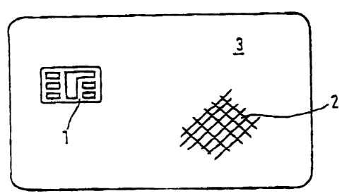
Fig. 1 shows an IC card with electronic module 1 in card
body 3 in a plan view. Card body 3 has dimensions which are
fixed in an ISO standard designated ISO 7810. Electronic mod-
ule 1 is embedded in the card body at a defined position
likewise fixed by an ISO standard designated ISO 7816/2. Ac-
cording to the invention card body 3 of the IC card is pro-
duced from one or a plurality of paper and/or cardboard lay-
ers.
Fig. 2 shows a multilayer card structure in cross sec-
tion prior to lamination of the individual card layers. The
card structure consists of upper cover layer 5, core layer 7
and lower cover layer 9. Core layer 7 is provided on both
sides with thin thermally activable adhesive layer 11 used
for gluing together the layers. Before the individual layers
are brought toqether, windows 13, 15 are punched in layers 5
and 7 so that a two-step gap arises in the card body, after
the three layers are brought together and glued. If a plural-
ity of core layers are used it is also possilala to pzoduce a
multistep gap in the card body, whereby the windows become
increasingly small in the individual cora layers, considered
from the upper cover layer. Such a card structure is espe-
cially advantageous when the casting compound of the elec-
tronic module has a drop shape, as shown e.g, in Fig. 9,
since the contours of the gap can then be readily adapted to
the shape of the casting compound and the bottom area of the
gap is small.
The card laminate can be produced in high throughputs.
Layers 5, 7 and 9 can thus be supplied from rolls and guided
for lamination through heated laminating rolls between which
the thernmally activable adhesive layers are activated. One
2 AUG.'96 9s3'I KLUNKER SCHMITT-NILSON HIRSCH DE """ " "=~"'y
- 7 21 82705
thus obtains an endless laminate provided at suitable inter-
vals with gaps for receiving the electronic modules. The in-
dividual card bodies are punched out of thia endless laminate
in a further method step. Electronic modules 7. are glued into
the card body gaps. The necessary adhesive can either be lo-
cated directly on the module or be introduced into the gap
e.g. in the form of liquid adhesive. The module can be incor-
porated in the card body before or after the card is punched
out.
To increase the bond strength between the module and the
card body one can, instead of using thermally activable adhe-
sive 11 located above the card layer, provide core layer 7
with cloth 8 impregnated with a thermally activable adhesive.
Fig. 2 indicates the cloth by the dots in upper thermally ac-
tivable layer 11. The cloth can be selected so as to allow
optimum bond strength between the electronic module and the
cazd body. in the finished card the cloth is thus located be-
tween cover layer 5 and core layer 7. The firm connection of
the module with the cloth thus anchors the module between the
card layers in the finished IC card. As an alternative to a
cloth located all over core layer 7, one can also provide a
cloth or foil only in the area of window 15 in core layer 7.
This will also achieve the abovementioned effects.
The module shown in Fig. 2 bears on surface 12 contact
surfaces for contacting communication. Alternatively the IC
card can also be provided with an electronic moduio suitable
for noncontacting data exchange. Such a module can be in-
serted in window 15. In this case one can thus dispenae with
window 13 in cover layer 5, so that in the finished IC card
the module for noncontacting data exchanqe is located in win-
dow
15 between cover layers 5 and S. Fig_ 3 shows tho card body of a single-9.ayer
cardboard
card in cross section. Cardboard 17 can likewise be supplied
from a roll. Windowe 15 are punched in the cardboard at suit-
able
intervals. Further, by debossing cardboard 17 in the
area of window 15 one produces shallow gap 19 whiCh has a.
2 AUG.'96 9sS2 KLUNKER SCHMITT-NILSON HIRSCH DE ip0766 S.70/49
~ 8 -
2182705
greater diameter than window 15. Electronic modul.e 1 can be
glued into the resulting gap in the cardboard, the bottom of
gap 19 being used as an adhesive layer. The module can again
be glued into the gap using an adhesive located on the mod-
ule, which can be a thermally activable adhesive or a contact
adhesive, or using a liquid adhesive. The card can be punched
out of the endleas cardboard before or after qluing. In the
finished IC card a part of window 15 which is not filled by
the module can be located in the module area on the back of
the card. To give the card a better appearance one can addi-
tionally close this part, e.g. by caating with a casting com-
pound or by other measures.
Fig. 4 again shows a multilayer card structure prior to
lamination in cross section. Layers 5, 7 and 9 are identical
with those from Fig. 2. In addition to these layers the
structure has separate adhesive layers 21 and 23 which are
also provided with suitable punchings.
Adhesive layers 21 and 23 can be formed either as ther-
mally activable layers or as contact adhesive layers. in the
latter case the windows must be produced in the layers when
the layers are still coated with a silicone band in order to
prevent the punching tools from sticking. After the punching
of the windows the silicone bands can be rolled off the con-
tact adhesive layers and onto other rolls.
Electronic module 1 can alzeady be inserted in the win-
dows of adhesive layer 21 prior to roll lamination in such a
way that the contact surface area lies on adhesive layer 21
and the area of the module receiving the integrated circuit
is located in the window, as shown in the figure. During
lamination of the shown card layers the shown module is thus
glued in the card bedy gap at the same time as adhesive layer
21_
If the electronic module is not to be glued in the gap
during lamination of the card body it is also possible to
punch out the window in adhesive layer 21 with exactly the
size of the window in cover layer S. In this case the shoul-
2 AUG. ' 96 9:32 KLUNKttt aCnMl i I-PIl LJt.1 V nL<JUn Ut n... w v. ,, i yy
9 2182705
=
der of the two-step gap remains free from the adhesive layer
during lamination of the layers so that no adhesive material
can penetrate onto the surface of the card during heating of
this layer. Such an embodiment is especially advantageous
when the punched-out card body is to be stared as an interme-
diate product. The card structure shown in Fig. 4 is also es-
pecially suitable for embedding a module for noncontacting
data exchange. In this case one can again dispense with the
windows in layers 5 and 21.
Figs. 2 and 4 show multilayer card structures in which
the individual layers already have windows before joining
which make up a gap in the card body after the layers are
joined. In contrast, Figs. 5 to 8 show embodiments in which
the gap is provided in the card body subsequently.
rig. 5 shows a card structure consisting of core layer 7
and cover layers 5 and 9, the layers being interconnected by
thermally activable adhesive layers 11. The thermally acti-.
vable adhesive layers used can be e.g. extremely thin poly-
ethylene (PE) foils or amorphous polyethylene terephthalate
(APET) foils, which are applied to core layer 7 on both
sides. In cover layer 5 one first produces with cutting tool
41 edge 43 which fixes the edge of the first part of a two-
step gap. One then uses a milling tool to produce two-step
gap 19 shown in Fig. 6 in the card body in such a way as to
expose thermally activable adhesive layer 11 on shoulder 45.
The use of a cutting tool for producing edge 43 has the
advantage that a clean and optically flawless edge arises in
the visible area of the finished chip card, whereas if one
uses a milling tool for producing a gap in the paper one can-
not avoid "fraying" on the edges, as indicated in Fig. 6 in
the edge area of the bottom part of the two-step gap. It is
of course also possible to dispense with the use of a cutting
tool and produce the gap solely with a milling tool.
An electronic module, as shown for example in Fig. 2, is
introduced into two-step gap 19 in the card body (see Fig. 6)
and glued on shoulder 45 with the help of thermally activable
c AUG.'96 9:33 KLUNKER 3CHMITT-NIL3ON HIRSCH Gt N:Ol00 J_ IL/47 = 10 2182705
adhesive layer 11 exposed during the milling process. It is
of course also possible to provide the electronic module ad-
with an adhesive to improve the bond with the card
ditionally
body. This is especially advantageous when thermally acti-
adhesive layers 11 are very thin and adhesive layer 11
vable
in shoulder area 45 of the gap is damaged or removed inten-
tionally or unintentionally during the milling process.
Fig. 7 shows the same layer structure as Fig. 5, but
cover layers 5 and 9 are not yet connected with core layer 7.
In the shown embodiment the card layers are interconnected
under the action of heat and pressure with heated dies 45 and
47, heated dies 45 and 47 having gaps 49 and 51 in the area
where the gap is subsequently produced in the card body. In
the area of these gaps thermally activable layers 11 are thus
not activated when the layers are connected so that no bond
is produced between the card layers in this area.
Fig. 8 shows the card structure from Fig. 7, the indi-
vidual card layers now being Lnterconnected. Due to the spe-
cial design of the heated dies cover layer 5 has not inter-
connected with core layer 7 in area 53, or cover layer 9 with
core layer 7 in area 55. Using cutting tool 41 one can now
produce the top part of a two-step gap by first introducing
cutting tool 41 into the card body at least far enough for
cover layer 5 to be severed_ The part of the cover layer lo-
cated within the edge of cut can then be easily removed siace
this part has not bonded with adhesive layer 11. The bottom
part of two-step gap 19 can be produced analogously using
cutting tool 57, One thus obtains a card body, as already
shown in Fig- 6, with a two-step gap which now has clean
edges of cut in the entire wall area. The described method is
of course not restricted to the production of a two-step gap.
One can also produce etepiess or multistep gaps in the card
body in analogous fashion.
The production method described in connection with Figs.
7 and 8 is suited especially for card bodies consisting ex-
clusively of paper and cardboard, since the individual paper
2 AUG.'96 9s34 KLUNKER SCHMITT-NILS[7N hLLtr.aun u= ffe,oo
2182705
~
layers are not softened during connection, as happens during
lamination of plastic layers. With the help of the shown
heated dies the heat is conducted only through the paper to
the thermally activable adhesive layers, which are then acti-
vated_ The paper layers themselves thus remain dimeasionally
stable throughout the production method, so that there is no
distortion of the paper layers whatsoever even at the transi-
tions to the unheated areas (see Fig. 7). The bottom area of
the two-step gap is thus very plane in the finished card
body.
Fig. 9 shows a single-laye~r card body with two-step gap
19 in which electronic module 1 is glued with liquid adhesive
59. in the daily use of chip cards there are bending loads
which act on the card body including the area of the elec-
tronic module. Due to these bending load3 and the aplittabil-
ity of paper, the paper in the embodiment shown in Fig. 9 can
split in shoulder area 45 (see Fig. 6) in gap 19 directly be-
low the liquid adhesive, so that the electronic module comes
out of the card body in the cou2se of time.
Although paper chip cards are preferably to be used for
applications in which the card need have only a short service
life, and a card structure as shown in Fig. 9 is thus basi-
cally durable enough, the compound between the electronic
module and the card body can be improved by providing two-
step gap 19 with undercuts 63 using suitable milling tool 61,
as shown in Fig. 10.
A dosed quantity of liquid adhesive 59 is introduced in
two-step gap 19, being distributed in gap 19 upon incorpora-
tion of electronic module 1 in such a way that undercuts 63
are also filled with liquid adhesive 59 (see Figs. 10 and
11). Thus electronic module 1 is anchored in the card body
and secured against forces acting perpendicular to the card
surface. Furthermore the liquid adhesive now moistening the
entire wall area of the gap also offers good protection
against splitting of the paper in this area. Alternatively it
is of coursQ also possible to dispense with undercuts and
2 AUG.'96 9134 KLUNKER SCHMITT-NILSGN HIRSCH DE Knroo ,y,7qiqy
-12- 2182705
=
dose the liquid adhesive so that it moistens the wall area
largely or completely in the finished card.
Fig, 12 again shows a multilayer card body prior to
lamination in cross section. Individual layers 5, 7 and 9 are
identical with the layers shown in Fig. 2. However upper
cover layer 5 has instead of window 13 two windows 25 sepa-
rated by bar 27. Befora lamination electronic module 1 is in-
serted in window 15 of core layer 7 in the way indicated in
Fig. 12. Duriag roll laminatioa of the layers module 1 is
glued to layer 7 and embedded additionally between layers 5
and 7. In the finished IC card the contact surfaces of module
1 are located in windows 25 and the embedding between the
layers brought about by bar 27. A module especially suitahle
for the abovementioned production technique is described ex-
actly in EP-B1 0 140 230.
Figs. 13 to 16 show further embodiments in which the
electronic module is already anchored in the card body during
production of the card by embedding parts of the module be-
tween two card layers.
Fig. 13 shows a multilayer card structure consisting of
cover layers 5 and 9 and core layers 7 and 8. Electronic mod-
ule 1 incorporated in the shown card structure has anchoring
frame 65 which protrudes beyond casting 67 of the imodule and
is already embedded between two card layers 5 and 7 during
production of the cards_ As shown in Fig. 13, anchoring frame
65 is surrounded on both sides by thermally activable adhe-
sive layers so that a good bond arises between the anchoring
frame and the card body. In a preferred embodiment the an-
choring frame is formed as a cloth into which adhesive mate-
rial from adjacent adhesive layers 11 can penetrate during
card production. This results in an indirect compound of ad-
jacent adhesive layers 11 and an improved anchoring of the
module in the card body.
Figs. 14 to 16 show further embodiments in which the
electronic module is embedded between two card layers. The
modules in these figures all have the same structure and are
2 AUG.'96 9s3S KLUNKER SCHMITT-NILSON HIRSCH DE gioayp g,~b/,49 13- 2182705
= {
referred to in general as lead frame modules. They consist of
metal wafer 69 in which a contact layout is formed and which
has applied to one side IC module 71 which is electrically
connected with the contact surfaces of the contact layout.
The IC module and electric connections are surrounded by a
casting Compound for protection from mechanical loads. In the
shorrn embodiments the anchoring frame is formed by extensions
of the contact surfaces which protrude beyond the actual con-
layout and are embedded between two card layers.
tact
Fig. 14 shows basically the same card structure as Fig.
13. The anchoring frame is alres.dy bent into the card inte-
rior during production of the card, i.e. during connection of
the individual layers, resulting in the structure shown in
Fig. 14. Production thus takes place analogously to the pro-
duction already explained in conjunction with Fig. 12.
Fig. 15 shows a chip card in cross section, wherein the
anchoring frame of the lead frame module is not bent and con-
tact surfaces 73 of the electronic module are located below
the card surface. The contact surfaces can be provided with
relief punchings 75 in the transitional area to the exten-
sions used for anchoring, so that they remain connected with
the extensions only by thin bars. This leads to a mechanical =
decoupling of the transitional area between module and an-
choring frame and thus to relief in this area upon bending
loads on the card, so that adhesive layer 11 does not come
off card layer 7 therebelow as quickly, e.g. due to tearing
or splitting of this card layer.
Fig. 16 shows basically the same cross section as Fig.
15. However, adhesive layer 11 extending below the anchoring
frame goes as far as the edge area of the bottom part of the
two-step gap, thereby obtaining a greater adhesive surface
for gluing the electronic module. Fig. 16 also shows heated
die 77 which can be used to further improve the compound be-
tween the anchoring frame and adhesive layers 11 in a sepa-
rate unit.
2 AUG.=96 9:36 KLUNKER SCHMITT-NILSON HIRSCH DE Wo'r6o 6.16/49
- 14 - 2102705
=
Fig. 17 finally shows a production method for a paper TC
card consisting of two layers connected by means of a contact
adhQsive_ In a first method step (Fig. 17a) compound elements
33 are pzodU.ced from contact adhesive band 31 coated with
silicone band 29. This is done by methods known from labeling
technology which are familiar to the expert and need not be
explained more cloeely here. Additionally the production of
such compound elements is known from l7E-OS 41 22 049. Sili-
cone band 29 provided with compound alements 33 is brought
together with paper layer 35 provided with contact adhesive
layer 37. Since the adhesion of the compound elemeat is
greater to the contact adhesive layer than to the silicone
layer, the compound element can be transferred to contact ad-
hesive band 37, yielding the intermediate product shown in
Fig. 17b. In a further method step (Fig. 17c) electronic mod-
ules 1 are punched out of module band 39 and glued to com-
pound element 33. The intermediate product shown in Fig. 17c
is brought together with prepunched cardboard band 17 with
windows 15 in such a way that the modules glued on paper
layer 35 come to lie in the windows. Finally, finished paper
IC cards 3 are punched out of the endless band, as shown in
Fig. 17e. it is of course also possible to manufacture the
paper card individually. In this case the individual card
layers shown in the figures are already card-sized, so that
one already obtains the card body in the desired dimensions
after connection of the individual layers.
The above statements always relate to embodiments in
which finished paper or cardboard webs are provided or
brought together and an electronic module inserted in the
card body at the same time or subsequently. Alternatively it
is also possible already to incorporate electronic modules in
the cardboard during production of the latter. This method
can be applied especially advantageously with electronic mod-
ules for noncontacting data exchange, e.g. consisting of a
ring-shaped coil and an integrated circuit electrically con-
nected with the coil, since these modules have lower require-
2 AUG.'96 9936 KLUNKER 6CHMITT-NILSON HIR3CH Dt HG/Op O.1//4L'
- 1S - 2182705
ments for positional accuracy in the finished data carrier
than modules for contacting data exchange. Further, the elec-
tronic modules for noncontacting data exchange are surrounded
on all sides by cardboard and embedded positively therein,
without elaborate measures having to be taken for producing a
channel for the module coil- The electronic modules are pref-
erably embedded in the cardboard in matrix form so that one
finally obtains a multiple-copy sheet or multiple-copy web
out of which individual data carriers with modules are
punched. The sheet can already be provided during production
with position markings to permit the punching tool to be po-
sitioned exactly so that, after punching, the electronic mod-
ule is positioned properly relative to the outside edqes of
the data carrier. It is further possible to provide the sheet
with a printed image before punching, so that the data car-
rier is already finished after punching. Alternatively it is
possible to provide the multiple-copy sheet bearing elec-
tronic modules for noncontacting data exchange with printed
cover layers on both sides and then to puncri out the individ-
ual data carriers. in this case the position markings for the
punching tool can be provided in the printed image of a cover
layer so that position markings in the cardboard can be dis-
pensed with.
One can take various measures which are explained in
connection with Figs. 18 to 21 to prevent splitting of the
paper or cardboard in the edge area of the punched-out paper
TC cards.
Fig. 18 shows in a plan view a detail of an endless band
having a multilayer structure, for example that shown in Fig.
in cross section. The core layer or layers of the multi-
layer card structure contain through holes 19 in the area
Where punching edge 81 of the card to be punched out is lo-
cated.
Fig. 19 showa a cross section along line A-A of Fig. 18.
During connection of the individual card layers material from
adjacent thermally activable adhesive layers 11 penetrates
2 AUG.'96 9237 KLLJNKER SCHMITT-NILSON HIRSCH DE rsio'!tib 5.18/49
AU -~6- 2182705
into the through holes so that cover layers 5 and 9 are indi-
rectly intezconnected. If one now punches the card out along
punching edge 81 in such a way that at least a part of each
through hole 79 is located in the card body, as indicated in
H'igs. 18 and 19, one obtains a oard edge which consists in
the core area alternately of paper or cardboard and adhesive
material from the adhesive layexs. This largely prevents
splitting of the core layer.
H'ig. 20 shows an already punched-out paper IC card in a
plan view. To protect the edge of the card from splitting,
special protecting lacquer 85 is applied thereto with spread-
ing unit 83. The cards can be processed either individually
or several in a stack simultaneously.
Fig. 21 shows a stack of card bodies 3 in cross section
to the edges of which protecting lacquer 85 is transferred
from transfer band 87 with the help of heated die 89 by the
transfer method.
The edges of the paper cards are preferably provided
with protecting lacquer if the cards have a single-layer card
structure, since in this case the method explained in con-
junction with Figs. 18 and 19 is unfeasible. Multilasyer cards
can of course also be provide.~~, with protecting lacquer,
whereby this lacquer can be the only, or an additional, pro-
tective measure against splitting of the card edge. The pro--
tecting lacquer can be colored and used as additional identi-
fication or an additional security feature.
Finally it should be mentioned that the layers forming
the cover layers of the card can already be provided with
printed imaqes, etc., completely or in certain areas before
production of the IC cards, whereby all common printing proc-
esses can be used such as relief embossing, offset printing,
steel gravure printing, screen printing, letterpress print-
ing, blind blocking, dough printing, wallpaper printing, hec-
tographic printing, etc. By using art paper one can further
increase the high printing quality already achievable on pa-
per, One can also include certain information (e.g. the
2 AUG.'96 9136 KWNKER SCHMITT-NIL5ON HIRSCH DE
- 1.7 -
n
21~Y2fl ~/5
credit balance of es new telephone card, etc.) in the printed
image in embossed printing, e.g. by eatbossing or by espe-
cially thick inking. In the finished card the external sur-
faces of the cover layers can be protected by a thin layer of
lacquer consisting e.g. of nitrocellulose lacquer, calender
lacquer, W-curing lacquer, electron-beam curing lacquer,
etc. The lacquer can be applied in the form of gloss lacquer
or matte lacquer. It is also possible to grain the layers of
lacquer.
Individual layers can additionally be provided with se-
curity elements, such as watermarks, scents, security
threads, fluorescent fibers in paper or cardboard, color cap-
sules in paper fibers, holograms, etc.
It is also especially easy to apply other elements to
paper cards, such as a magnetic track by applying a water-
base magnetic lacquer or a match rubbing surface.
Finally, threads can be worked into the thicker paper
layers or cardboard layers during production of these layers
to make these layers less likely to split. Suitable tech-
niques are known from paper processing and will not be ex-
plained more closely here.'For connecting the individual pa-
per or cardboard layers one can use not only thermally acti-
vable adhesives but also contact adhesives or liquid adhe-
sives. To preveat splitting of the paper or cardboard in the
area of the gap for the module one can strengthen these areas
by cloth, liquid adhesivea or resina.