Note: Descriptions are shown in the official language in which they were submitted.
218282~
APPARATUS FOR AND METHOD OF SUPPRESSING
POWER SURGES UTILIZING ELECTRICAL STRIPLINES
Inventor: Albert Zaretsky
BACKGROUND OF THE INVENTION
Today, it is well known that surges in electrical power may appear, from time totime, in electric utility power distribution systems and within residential, commercial and
industrial electrical power systems. An electrical power surge potentially could have a
current magnitude as high as a few thousand amperes and a time duration as short as a
few microseconds. Electrical power surges potentially contain sufficient energy to
destroy unprotected or poorly protected equipment connected to the electrical system.
In order to protect connected electrical equipment from being damaged or
destroyed upon the occurrence of power surges, devices known as transient voltage surge
suppressors (TVSSs) are commonly employed. TVSS devices are typically connected in
parallel with a device or circuit to be protected. Upon the occurrence of a power surge,
these surge su~ essing devices clamp the voltage impressed across their terminals to a
predetermined value. Metal Oxide Varistors (MOVs) or gas discharge tubes are typically
utilized as surge suppressor components and exhibit voltage clamping properties.The effectiveness of a TVSS device in clamping transient surges is measured at the
device outer termin~l~. The voltage clamping level of the surge suppressing components,
such as MOVs, is degraded by the wiring between the components and the device
termin~ . In other words, the protected equipment "sees" less protection at the circuit
terminals than the TVSS components are capable of providing. This reduction in surge
suppression protection at the terminals of a TVSS device is caused by the inductance in
the wires or cables connecting TVSS components to the device (referred to herein as a
surge suppressor) external termin~l~. A TVSS circuit includes a finite length of wire or
2182827
`_
cable to connect the circuit board tçrmin~lc to the surge supl)lessillg device external
termin~lc. Wire or cable is typically used which exhibits a relatively high value of
inductance, even for low gauge wire or bus bar. During high current surges (i.e., from
transient overvoltages), a significant voltage develops across the cable due to its inherent
inductance. At the circuit, voltage is clamped at the TVSS rated clamping voltage plus
the voltage developed due to the inductance in the cable, greatly ~iminiching the effective
surge clamping ability (i.e., voltage) at the external terminals of the surge ~pressing
device.
The instantaneous voltage V across an inductor having inductance L is given by
the well known relationship, V=L*di/dt, where di/dt is the instantaneous change in
current divided by the instantaneous change in time. Thus, for short duration, high
current surge pulses, even the relatively smali inductance of standard # 12 or #14 gauge
wire or bus bar causes a large voltage to be generated. For example, a terminal board
might include 12 inches of #12 gauge cable having an inductance of 0.3 IlH/ft for
connecting the board's tçtmin~lc to the TVSS device thereon. The inductance of both the
input and return wire would therefore be 0.6 ,u~I. A surge current pulse having a duration
of 8 ,us and a magnitude of 3000 amperes would generate a voltage of 225 V in the cable
due to the inductance. Thus, a TVSS circuit incorporating an internal surge suppressor
device circuit rated at its pins at 400 V could only provide protection of 625 volts at its
circuit termin~lc, i.e., 625 volt clamping protection instead of 400.
Conventional attempts to provide a solution to this problem typically focus on
increasing the current handling capability of the electrical connection between the
suppressor external tçtmin~l contacts and the surge ~u~plessor components. For example,
low impedance heavy gauge copper bus barsl are used instead of wire or cable. Although
the resistivity of the connection is reduced, the inductance is only slightly affected. Thus,
there is still a large inductive reactance in the bus bars and as a result of any large change
in ~ ellt over time, e.g., a short time, thereby generating an unacceptably large voltage
``` 2182827
at the external connections. Accordingly, there is a need for improved connections for
connecting a TVSS component to external line power such that the voltage generated
across this connection (i.e., a connection which preferably displays a minim~l inductance)
during a power surge is minim~l.
OBJECTS AND SUMl\~ARY OF THE INVENTION
It is therefore an object of the present invention to overcome the above-mentioned
shortcomings of the prior art.
It is another object of the present invention to provide a method and apparatus for
su~lessi,lg power surges which minimi7e a voltage generated in a conductive pathconnecting the TVSS device to a source of power thereby maximizing TVSS protection
for equipment connected at the power source.
It is another object of the present invention to provide a method and apparatus for
sul~prcssing power surges which include means for providing a conductive path which
displays a minimum inductance such that a voltage induced across the inductance during
a transient power surge is a ~
It is still another object of the present invention to provide a method and appal~us
for s~ essillg power surges which utilize stripline cir~iuill y to provide a conductive path
between a source of power and a TVSS device such that a minimum inductive reactance
is generated in the stripline during a transient power surge.
Apparatus of the present invention utilizes stripline techniques for suppressingtransient voltage surges normally induced in conductive paths connecting a power source
to a TVSS device. More particularly, the inductance and capacitance characteristics of
the electrical conductive path connecting the surge ~uppressor components to the external
line power are improved by the stripline means implemented according hereto. While
typically associated with high frequency, low power applications such as UHF, VHF,
microwave and millimeter wave circuils, stripline techniques provide for controlling the
2~828~7
characteristic impedance, in particular, the inductance, of the conductive path formed
thereby. One advantage of using stripline circ~ to connect a TVSS to a circuit for
protection is that it elimin~tes the need to place the surge suppressor (TVSS) very close to
the terminals of the circuit board upon which it resides, a typical if not overly effective
effort found in the prior art for attempting to reduce the magnitude of voltages (directly
related to length) generated in the connecting cable. Thus, flexibility is increased as to
the mechanical layout of the TVSS device relative to the protected circuitry. This is a big
advantage over conventional bus bars and ordinary copper wiring which restrict board
layout because of their inherent inductance and a~e faced with unacceptable induction-
induced voltages present in the wires during over-voltage surging.
In one embodiment, a transient voltage surge suppressor circuit or system is
provided which includes an input terminal coupled using a stripline conductor from a
source of electrical power to a surge suppressor component for clamping the source line
voltage to a predetermined value. The electrical stripline conductor acts to minimi7e the
inductance and thus the characteristic impedance of the electrical connection between the
input termin~l and the surge suppressor device. The result is an increased clamping
voltage effectiveness at the input terminal to the ~u~plcssor circuit.
BRIEF DESCRIPTION OF THE DRAWINGS
Fig. 1 is a functional block diagram of a preferred embodiment of the present
invention;
Fig. 2 is a schematic diagram of the preft;lled embodiment of the present invention
of Figure 1;
Fig. 2A is a schematic diagram of the cross sectional view of the embodiment
depicted in Fig. 2; and
Fig. 3 is a functional block diagram of another embodiment of the present
invenffon which provides for protection in a three phase electrical power circuit.
DETAILED DESCRIPTION OF THE INVENTION
- ~18~82~
.
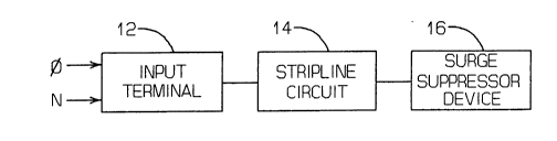
A transient voltage surge supprcssor circuit 10 (hereinafter referred to
interchangeably as su~essor or TVSS circuit) of the present invention is shown in
Figure 1. Phase and neutral terminals of an external electrical power source (not shown
in the figure) are connectable as shown to an input terminal 12 of the suppressor circuit
10. A conventional surge s~ressor device 16 functions to clamp the line voltage to a
predetermined voltage value upon the occurrence of a power surge and is coupled to the
input terminal via stripline circuit 14. Surge suppressor device 16 may employ, for
example, solid state surge ~ cssors, such as MOVs, gas discharge tubes, etc. Stripline
circuit 14 is lltili7ed herein to electrically connect the surge suppressor device 16 to input
te~ l 12. The stripline circuit controls the characteristic impedance (ZO)~ i.e., the
combined induct~nce, capacitance and resistance, of the conductive path. Although
stripline techniques are traditionally associated with high frequency, low powerapplications, such as RF and radar, the present invention has applied stripline techniques
to low frequency, high power applications, e.g., 120 V, 60 Hz single and multiple phase
AC power TVSS devices.
A more detailed view of the structure of surge sll~)pressor circuit 10 is shown in
Fig. 2. An electrical power source 22is shown therein, identifying both phase and neutral
lines which are connected to circuit input terminal 12 and a load (i.e., a circuit requiring
overvoltage protection) 21. Also connected to terminal 12 is a length of the stripline, i.e.,
a stripline circuit 14, coupling power from power source 22 to the TVSS device 16.
Stripline circuit 14 consists oftwo parallel stripline conductors 18, 20 located very close
to one another and separated by a dielectric 17 to realize high magnetic flux cancellation
and extremely low inductance. A preferred gap between two stripline conductors 6inches in length is around 4 mils since standard 4 mil mylar facilitates low impedance and
5000 volt dielectric capability. The length of stripline is preferably kept as short as
possible to reduce its inductance (i.e., impedance). Surge ~ essor device 16 is
electrically coupled to stripline circuit 14 at the other ends of stripline conductors 18, 20.
` ' 21g~827
A cross-sectional view of a portion of stripline circuit 14 of Fig. 2 will now be
described with reference to Fig. 2A. The electrical characteristic (the circuit's
characteristic impedance) is determined by the dimensions of stripline conductors 18, 20,
the properties of the conductive material, and the properties of the insulating film or
printed circuit board or dielectric 17 upon which the stripline conductors are mounted.
The distance between stripline circuils 18, 20 and their respective thickness and widths
determine, to a large extent, the flux canceling capability and inherent inductance of
stripline circuit 14. For example, 5/8" wide strips, .011" thickness, 12" long and
separated by 4 mil thick mylar.
To achieve the high current carrying capability required of an industrial or
commercial grade TVSS device (e.g., the ability to handle 3000 ampere surges), the width
of striplines 18, 20 is relatively wide. For example the stripline described above only
added 7 volts clamping for a 12" length and 3000 amp 8 x 20 transient pulse. Much
lower inductance values for the connection (i.e., corresponding to lower voltages induced
within the stripline circuit 14) were achieved by widening the stripline conductors 18, 20
rather than by increasing their thickness. Increasing the thickness of a bus bar does not
achieve as large a flux cancellation and subsequent lower inductance values as does
widening a thin stripline conductor.
While TVSS device 10 of Figure 1 is shown connected to a source of single phase
electrical power, the invention is also useful in three phase applications, as exemplified
by the illustration of Figure 3. Shown therein are each of three phase, neutral and ground
ports for connecting telmin~l 24 to the three-phase source. Three-phase input terminal 24
feeds the potential found at each of three ports to a three phase stripline circuit 26, which
electrica!ly couples the potential thereby to three-phase surge ~u~pressor device 28.
Three-phase surge ~u~plessor device 28 may be implemented by any conventional surge
~u~ ssor technology known to those skilled in the art for clamping energy during power
surges. Each incoming electrical phase is associated with an individual stripline
.
- ~182827
conductor 18, 20, 32. The distance b~l~een the phase and neutral, phase and ground, or
phase to phase stripline conductors, their thickness and width are all optimized to
minimi7.e the resultant inductance of each stripline conductor, and therefore the
impedance seen by the surge ;ulle~
During development of the plese ll invention, several laboratory tests were
pc.ro~ ed using different stripline conductor configurations of electrically conductive
material and each configuration's various associated dimensions. The test circuit used
was similar to the circuit shown in Figure 2. Electrical power source 22 was replaced
with a surge generator for generating standard underwriter lab category B unipolar pulses.
Category B unipolar test pulses include 3000 A, 8 x 20 surge pulses and 6000 V, 1.2 x 50
pulses. The current pulses, applied to shorted suppressor device terminals rise to a
magnitude of 3000 A in 8 lls and decay to half their value in 20 ,us. The resultant voltage
pulses, when applied to open termin~l~, rise to a magnitude of 6000 V in 1.2 ~s and decay
to half their value in 50 lls. The length of electrical conductor ( i.e. stripline, wire or bus
bar) used for all laboratory tests was 12 inches. For each surge ~u~ressor device
connection configuration, the ~u~lession voltages detecte~ at surge ~upl)ressor device 16
and at the surge ~plessor circuit input terminal 12 were measured. The difference
between the two detected voltages is listed in the table below.
VVIRING CONFIGURATION VOLTAGE Dl~;KENCE
Random #14 gauge wires 214 V
#14 gauge wires 1 inch apart in parallel 165 V
Bus Bars 3 inches apart 147 V
Double sided G10 PC board material, 1/16 44 V
inch thick, 1/2 inch wide strips, 2 oz.
copper
Copper bars, 0.061 inches thick, 0.484 13 V
inches wide, 4 mil mylar dielectric
Copper tape, 0.010 inches thick, 0.594 14 V
inches wide, 13 mil mylar dielectric
Copper tape, 0.011 inches thick, 0.625 7 V
inches wide, 4 mil mylar dielectric
-- 2~8~827
The results shown above reveal a dramatic decrease in the voltage generated across
the connecting conductor by switching from random gauge wires to stripline conductors.
It is a~pa~cnt from the results that the stripline technique is more effective than copper
bus bars in reducing clamping voltage loss. The results also dr2m~ti7e the very limited
results achieved by decreasing resistivity (switching from #14 gauge wires to bus bars
three inches apart) rather than decreasing conductor indllct~nce.
The description of the present invention, as described herein, was for illustrative
purposes only and is not meant to limit the scope or spirit of the invention thereto.